EP0534007B1 - Differenzverstärkeranordnung - Google Patents
Differenzverstärkeranordnung Download PDFInfo
- Publication number
- EP0534007B1 EP0534007B1 EP91202503A EP91202503A EP0534007B1 EP 0534007 B1 EP0534007 B1 EP 0534007B1 EP 91202503 A EP91202503 A EP 91202503A EP 91202503 A EP91202503 A EP 91202503A EP 0534007 B1 EP0534007 B1 EP 0534007B1
- Authority
- EP
- European Patent Office
- Prior art keywords
- voltage
- current
- differential amplifier
- vref
- differential
- Prior art date
- Legal status (The legal status is an assumption and is not a legal conclusion. Google has not performed a legal analysis and makes no representation as to the accuracy of the status listed.)
- Expired - Lifetime
Links
- 230000001105 regulatory effect Effects 0.000 claims description 7
- 238000010079 rubber tapping Methods 0.000 claims description 4
- 230000008859 change Effects 0.000 description 5
- 230000001276 controlling effect Effects 0.000 description 5
- 230000004048 modification Effects 0.000 description 4
- 238000012986 modification Methods 0.000 description 4
- 230000001419 dependent effect Effects 0.000 description 2
- 230000000694 effects Effects 0.000 description 2
- 230000004044 response Effects 0.000 description 2
- 238000013459 approach Methods 0.000 description 1
- 238000013461 design Methods 0.000 description 1
- 238000000034 method Methods 0.000 description 1
- 230000008569 process Effects 0.000 description 1
- 238000012545 processing Methods 0.000 description 1
- 230000009467 reduction Effects 0.000 description 1
- 238000012546 transfer Methods 0.000 description 1
Images
Classifications
-
- H—ELECTRICITY
- H03—ELECTRONIC CIRCUITRY
- H03F—AMPLIFIERS
- H03F3/00—Amplifiers with only discharge tubes or only semiconductor devices as amplifying elements
- H03F3/45—Differential amplifiers
- H03F3/45071—Differential amplifiers with semiconductor devices only
- H03F3/45076—Differential amplifiers with semiconductor devices only characterised by the way of implementation of the active amplifying circuit in the differential amplifier
- H03F3/45179—Differential amplifiers with semiconductor devices only characterised by the way of implementation of the active amplifying circuit in the differential amplifier using MOSFET transistors as the active amplifying circuit
-
- H—ELECTRICITY
- H03—ELECTRONIC CIRCUITRY
- H03F—AMPLIFIERS
- H03F1/00—Details of amplifiers with only discharge tubes, only semiconductor devices or only unspecified devices as amplifying elements
- H03F1/32—Modifications of amplifiers to reduce non-linear distortion
- H03F1/3211—Modifications of amplifiers to reduce non-linear distortion in differential amplifiers
-
- H—ELECTRICITY
- H03—ELECTRONIC CIRCUITRY
- H03F—AMPLIFIERS
- H03F3/00—Amplifiers with only discharge tubes or only semiconductor devices as amplifying elements
- H03F3/45—Differential amplifiers
- H03F3/45071—Differential amplifiers with semiconductor devices only
- H03F3/45076—Differential amplifiers with semiconductor devices only characterised by the way of implementation of the active amplifying circuit in the differential amplifier
- H03F3/45179—Differential amplifiers with semiconductor devices only characterised by the way of implementation of the active amplifying circuit in the differential amplifier using MOSFET transistors as the active amplifying circuit
- H03F3/45183—Long tailed pairs
-
- H—ELECTRICITY
- H03—ELECTRONIC CIRCUITRY
- H03F—AMPLIFIERS
- H03F3/00—Amplifiers with only discharge tubes or only semiconductor devices as amplifying elements
- H03F3/45—Differential amplifiers
- H03F3/45071—Differential amplifiers with semiconductor devices only
- H03F3/45479—Differential amplifiers with semiconductor devices only characterised by the way of common mode signal rejection
- H03F3/45632—Differential amplifiers with semiconductor devices only characterised by the way of common mode signal rejection in differential amplifiers with FET transistors as the active amplifying circuit
- H03F3/45636—Differential amplifiers with semiconductor devices only characterised by the way of common mode signal rejection in differential amplifiers with FET transistors as the active amplifying circuit by using feedback means
- H03F3/45681—Measuring at the common source circuit of the differential amplifier
- H03F3/4569—Controlling the common source circuit of the differential amplifier
-
- H—ELECTRICITY
- H03—ELECTRONIC CIRCUITRY
- H03F—AMPLIFIERS
- H03F3/00—Amplifiers with only discharge tubes or only semiconductor devices as amplifying elements
- H03F3/45—Differential amplifiers
- H03F3/45071—Differential amplifiers with semiconductor devices only
- H03F3/45479—Differential amplifiers with semiconductor devices only characterised by the way of common mode signal rejection
- H03F3/45632—Differential amplifiers with semiconductor devices only characterised by the way of common mode signal rejection in differential amplifiers with FET transistors as the active amplifying circuit
- H03F3/45695—Differential amplifiers with semiconductor devices only characterised by the way of common mode signal rejection in differential amplifiers with FET transistors as the active amplifying circuit by using feedforward means
- H03F3/4573—Measuring at the common source circuit of the differential amplifier
- H03F3/45739—Controlling the loading circuit of the differential amplifier
-
- H—ELECTRICITY
- H03—ELECTRONIC CIRCUITRY
- H03F—AMPLIFIERS
- H03F2203/00—Indexing scheme relating to amplifiers with only discharge tubes or only semiconductor devices as amplifying elements covered by H03F3/00
- H03F2203/45—Indexing scheme relating to differential amplifiers
- H03F2203/45008—Indexing scheme relating to differential amplifiers the addition of two signals being made by a resistor addition circuit for producing the common mode signal
-
- H—ELECTRICITY
- H03—ELECTRONIC CIRCUITRY
- H03F—AMPLIFIERS
- H03F2203/00—Indexing scheme relating to amplifiers with only discharge tubes or only semiconductor devices as amplifying elements covered by H03F3/00
- H03F2203/45—Indexing scheme relating to differential amplifiers
- H03F2203/45074—A comparator circuit compares the common mode signal to a reference before controlling the differential amplifier or related stages
-
- H—ELECTRICITY
- H03—ELECTRONIC CIRCUITRY
- H03F—AMPLIFIERS
- H03F2203/00—Indexing scheme relating to amplifiers with only discharge tubes or only semiconductor devices as amplifying elements covered by H03F3/00
- H03F2203/45—Indexing scheme relating to differential amplifiers
- H03F2203/45078—Indexing scheme relating to differential amplifiers the common mode signal being taken or deducted from the one or more inputs of the differential amplifier
-
- H—ELECTRICITY
- H03—ELECTRONIC CIRCUITRY
- H03F—AMPLIFIERS
- H03F2203/00—Indexing scheme relating to amplifiers with only discharge tubes or only semiconductor devices as amplifying elements covered by H03F3/00
- H03F2203/45—Indexing scheme relating to differential amplifiers
- H03F2203/45466—Indexing scheme relating to differential amplifiers the CSC being controlled, e.g. by a signal derived from a non specified place in the dif amp circuit
-
- H—ELECTRICITY
- H03—ELECTRONIC CIRCUITRY
- H03F—AMPLIFIERS
- H03F2203/00—Indexing scheme relating to amplifiers with only discharge tubes or only semiconductor devices as amplifying elements covered by H03F3/00
- H03F2203/45—Indexing scheme relating to differential amplifiers
- H03F2203/45612—Indexing scheme relating to differential amplifiers the IC comprising one or more input source followers as input stages in the IC
-
- H—ELECTRICITY
- H03—ELECTRONIC CIRCUITRY
- H03F—AMPLIFIERS
- H03F2203/00—Indexing scheme relating to amplifiers with only discharge tubes or only semiconductor devices as amplifying elements covered by H03F3/00
- H03F2203/45—Indexing scheme relating to differential amplifiers
- H03F2203/45641—Indexing scheme relating to differential amplifiers the LC being controlled, e.g. by a signal derived from a non specified place in the dif amp circuit
-
- H—ELECTRICITY
- H03—ELECTRONIC CIRCUITRY
- H03F—AMPLIFIERS
- H03F2203/00—Indexing scheme relating to amplifiers with only discharge tubes or only semiconductor devices as amplifying elements covered by H03F3/00
- H03F2203/45—Indexing scheme relating to differential amplifiers
- H03F2203/45648—Indexing scheme relating to differential amplifiers the LC comprising two current sources, which are not cascode current sources
Definitions
- the present invention relates to a differential amplifier arrangement including a differential pair comprising two individual amplifier branches with first and second input terminals, said amplifier branches including a first and a second input transistor respectively, said amplifier branches being connected to a common branch including a current source, and a junction point which is connected to the sources/emitters of said first and second input transistors and the current of said current source being regulated by a control circuit so as to linearize an input/output characteristic of said differential pair.
- Such a differential amplifier arrangement is already known in the art, e.g. from the book "Analogue IC design : the current-mode approach", edited by C. Tomazou et al, IEE circuits and systems series 2, 1990, pages 197-202, and more particularly figure 5.12 thereof.
- the control circuit is used to linearize the input voltage/output current characteristic of differential pair. This linearization is obtained by keeping the gain or the transconductance (gm) of the amplifier independent of the differential input voltage across the input terminals.
- control circuit includes an auxiliary differential pair of NMOS transistors which are controlled by the first and the second input terminals and of which the drain currents are applied in common via a mirror circuit to the gate electrode of a third NMOS transistor included in the common branch and constituting the regulated current source.
- the source electrodes of the NMOS transistors of the auxiliary differential pair are connected to a common voltage terminal to which a constant DC voltage source needs to be connected.
- control circuit is a feed forward circuit which puts stringent demands on the matching of all the MOS transistors of the arrangement in order to achieve the requested linearity.
- MOS transistors of the individual amplifier branches and these of the auxiliary differential pair have to match perfectly, as well as the PMOS transistors of the mirror circuit and the NMOS transistor of the mirror circuit with the third NMOS transistor. This leads to process constraints which are difficult to achieve.
- An object of the present invention is to provide a differential amplifier arrangement of the above known type, but wherein the linearization of the input/output characteristic is achieved with matching a minimum number of active devices of the arrangement.
- control circuit includes a negative feedback circuit with a comparator whose inputs are connected to a reference terminal to which a reference voltage is applied and to said junction point, and whose output controls said current source.
- the negative feedback circuit modifies the current of the current source so as to align the voltage at the junction point to the reference voltage.
- Another object of the present invention is to obtain the requested linear characteristic in a simple way without requiring an ideal voltage source, such a source being not easy to realize in practice.
- this other object is achieved due to the fact that said comparator is an operational amplifier having a non-inverting and an inverting input, said junction point and said reference terminal being connected to said non-inverting and inverting inputs respectively.
- the differential amplifier arrangement only receives perfectly symmetrical input signals across the differential first and second input terminals. This is however not always the case in practice and the linearization can then only be obtained by keeping the transconductance (gm) independent of the common mode voltage across the input terminals.
- a further object of the present invention is to provide a differential amplifier arrangement of the above known type but which linearizes the input/output characteristic even when not symmetrical differential input signals are applied to the input terminals.
- this further object is achieved due to the fact that said reference terminal is so coupled to said input terminals that said reference voltage follows the common mode voltage on said input terminals.
- said control circuit further includes a first and a second interface means and a voltage divider, and that said reference terminal is a tapping point of said voltage divider whose input terminals are coupled through said first and second interface means to said first and second input terminals respectively.
- the transconductance remains independent of the common mode voltage.
- Still another object of the present invention is to obtain an adjustable gain or transconductance (gm) of the differential amplifier arrangement.
- gm transconductance
- control circuit further includes means to derive said reference voltage as a sum of said common mode voltage and a predetermined voltage.
- the transconductance (gm) is modified by modifying the voltage at the junction point. Because the latter voltage follows the reference voltage the control circuit associated with this reference voltage allows not only the linearization of the above characteristic but also the modification of the slope thereof.
- first and second interface means are respectively connected in series with a second and third current sources, said output terminals of said voltage divider being connected to the junction points of said first interface means and said second current source and of said second interface means and said third current source, respectively, the current in said second and third current sources being regulated via a control input terminal through which said predetermined voltage is adjusted.
- the current in both the second and third current sources is modified. This leads to a variation of the voltage across the interface means, i.e. between the first/second input terminal and the input terminals of the voltage divider. As a result, the reference voltage, and thus also the voltage at the junction point, are modified This voltage change at the junction point does not harm the above linearity since it is independent of the differential input voltage across the first and second input terminals.
- Another object of the present invention is to suppress the common mode output current in the individual amplifier branches.
- the differential amplifier arrangement further includes current mirror circuitry controlled by said control circuit and of which the outputs are coupled to said individual amplifier branches for suppressing common mode output currents therein.
- said current mirror circuitry includes a fourth current source connected in series with a current mirror and a fifth and a sixth current sources connected in series with distinct ones of said individual amplifier branches and controlled by said current mirror.
- the control circuit together with the current mirror circuitry eliminate the common mode output current in the following way.
- the control circuit modifies the reference voltage and thereby the voltage at the junction point by controlling the current of the first current source.
- a common mode output current is generated in the individual amplifier branches.
- this current is counterbalanced by a replica thereof which is generated by the current mirror circuitry under the control of the control circuit and which is also flowing through the individual amplifier branches but in the reverse direction.
- the operational transconductance amplifier OTA shown is used as a basic building block in active analogue integrated filters where it is generally used in combination with a capacitance (not shown). It is then known as an OTA-C pair producing one pole, the location of the latter being linearly dependent on the overall transconductance gm of the amplifier. Hence, by modifying gm, the location of the pole can be changed and the OTA-C pair can be tuned to have a particular frequency response.
- the operational transconductance amplifier OTA is a differential input voltage to a differential output current transducer with an adjustable overall transconductance gm.
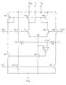
- OTA has differential voltage input terminal VG1 and VG2 and differential current output terminals I1 and I2. It mainly includes, coupled between power supply terminals VDD and VSS at which, e.g., 5 Volts and 0 Volt are respectively supplied, a differential pair of two individual amplifier branches each constituted by the drain-to-source path of a NMOS transistor M1/M2 and connected in common at a junction point VS to the drain electrode of another NMOS transistor M3 of which the source electrode is connected to VSS.
- OTA includes between the terminals VDD and VSS, two branches which are each constituted by the series connection of the drain-to-source paths of NMOS transistors M8/M9 and M10/M11 respectively.
- the junction point VX of M8 and M10 is coupled to the junction point VY of M9 and M11 via a voltage divider constituted by the series connection of two identical resistors R1 and R2.
- the tapping point Vref of this voltage divider is connected to the inverting input (-) of a differential amplifier A to the non-inverting input (+) of which the junction point VS is connected and of which the output is connected to the gate electrode of the NMOS transistor M3.
- the input terminals VG1,VG2 are connected to the gate electrodes of the NMOS transistors M8,M9 respectively, whilst a control input terminal VC is connected to the gate electrodes of both the NMOS transistors M10 and M11.
- Voltages VG1, VG2, VS, VX, VY and Vref and currents I1 and I2 are present at the like-named terminals.
- a first goal of the above described control circuit is to linearize the differential input voltage (VG2 - VG1) versus differential output current (I2 - I1) characteristic of the differential amplifier OTA.
- This linearization allows the differential amplifier to handle large signals, e.g. of 2.5 Volts peak-to-peak, without distortion.
- the overall transconductance gm of the differential amplifier is kept constant by maintaining the common voltage VS at the like-named junction point equal to the reference voltage Vref. This is realized by the operational amplifier A acting as a comparator for the two latter voltages and controlling the gate electrode of transistor M3 operating as a regulated current source able to modify the common voltage VS.
- Id k (VG - VS - VT) 2
- Id the drain current
- VG the gate voltage
- VT the threshold voltage
- k a conductance parameter dependent on processing parameters such as ⁇ and Cox of the MOS transistor of an amplifier branch, VS being the above common voltage.
- the common mode input voltage is transmitted from VG1, VG2 to the terminals VX, VY via the gate-to-source path of the source-follower transistors M8/M9 acting then as interface means.
- This common mode input voltage then appears at the voltage terminal Vref and thus also at the junction point VS owing to the comparator A and the regulated current source M3.
- Vref follows the common mode input voltage (VG1 + VG2)/2 as explained above
- another voltage e.g. a DC voltage
- Vref another voltage
- a DC voltage may be added (or substracted) to Vref for obtaining a predetermined transconductance gm.
- This additional voltage is supplied to Vref as derived from a control voltage VC applied to the like-named control input terminal.
- the latter control voltage VC controlling the currents flowing through both the NMOS transistors or current sources M10 and M11 whereby the voltages VX and VY are modified.
- the reference voltage Vref is modified in function of VC and the value of gm changes accordingly.
- the already described operational transconductance amplifier OTA further includes a common mode output current rejection circuit which is controlled by the comparator A so as to adjust common mode currents in the individual amplifier branches including the NMOS transistors M1 and M2.
- This circuit includes, between the voltage supply terminals VDD and VSS, the series connection of a diode connected PMOS transistor M6 with the drain-to-source path of NMOS transistor M7, the output of the operational amplifier A being connected to the gate electrode of M7. Furthermore, a PMOS transistor M4/M5 is inserted between the voltage supply terminal VDD and the drain electrode of the NMOS transistor M1/M2 of each of the individual amplifier branches, the gate and source electrodes of M6 being connected in common to the gate electrodes of both the transistors M4 and M5.
- This last circuit is to remove the common mode output current from the differential outut currents I1 and I2 taken at the drain electrodes of M1 and M2 respectively.
- This unwanted common mode output current is generated by the controlling action of the above negative feed back loop of the control circuit. Indeed, any change of the common mode input voltage would lead, as explained above, to a change of the reference voltage Vref and thus also to a change of the common voltage VS at the like named junciton point. As a consequence, the modification of VS leads to the generation of a common mode current in the two amplifier branches and this current will appear in the output current causing damages to the following circuits.
- the present circuit generates a replica from the common mode current and this replica is injected into the two amplifier branches to counterbalance the unwanted common mode current.
- the current source M7 is controlled by the output of the comparator A - which also control the current source M3 for modifying the common voltage VS - and the current generated by M7 is mirrored via M6 to the current sources M4 and M5 which in turn generate the replica of the unwanted common mode output current. This latter current is thereby removed from the differential output currents I1 and I2.
- the present amplifier OTA is entirely integrated in an electronic chip and is able to handle signals over a large frequency range extending from audio to a few MHz.
Landscapes
- Engineering & Computer Science (AREA)
- Power Engineering (AREA)
- Physics & Mathematics (AREA)
- Nonlinear Science (AREA)
- Amplifiers (AREA)
- Networks Using Active Elements (AREA)
- External Artificial Organs (AREA)
- Solid-Sorbent Or Filter-Aiding Compositions (AREA)
Claims (12)
- Differenzverstärkerschaltung ein Differenzpaar (M1, M2) enthaltend, das zwei einzelne Verstärker zweige mit ersten (VG1) und zweiten (VG2) Eingangsanschlüssen umfaßt, wobei die Verstärkerzweige einen ersten (M1) beziehungsweise einen zweiten (M2) Eingangstransistor enthalten, wobei die Verstärkerzweige mit einem gemeinsamen Zweig verbunden sind, der eine Stromquelle (M3) sowie einen Verbindungspunkt (VS) umfaßt, welcher mit den Source-/Emitter-Elektroden des ersten und zweiten Eingangstransistors verbunden ist, und wobei der Strom der Stromquelle durch eine Steuerschaltung (A; R1, R2; M8, M9; M10, M11) geregelt wird, um so die Eingangs-/Ausgangs-Kennlinie des Differenzpaares zu linearisieren, dadurch gekennzeichnet, daß die Steuerschaltung (A; R1, R2; M8, M9; M10, M11) eine negative Rückkopplungsschaltung mit einem Komparator (A) enthält, dessen Eingänge mit einem Referenzanschluß (Vref), an den eine Referenzspannung (Vref) angelegt wird, und mit dem Verbindungspunkt (VS) verbunden sind und dessen Ausgangssignal die Stromquelle (M3) steuert.
- Differenzverstärkerschaltung gemäß Anspruch 1, dadurch gekennzeichnet, daß der Komparator (A) ein Operationsverstärker ist, der einen nichtinvertierenden (+) und einen invertierenden (-) Eingang besitzt, wobei der Verbindungspunkt (VS) und der Referenzanschluß (Vref) an den invertierenden beziehungsweise den nichtinvertierenden Eingang angeschlossen sind.
- Differenzverstärkerschaltung gemäß Anspruch 1, dadurch gekennzeichnet, daß der Referenzanschluß (Vref) derart an die Eingangsanschlüsse (VG1, VG2) angeschlossen ist, daß die Referenzspannung (Vref) der Gleichtaktspannung an den Eingangsanschlüssen folgt.
- Differenzverstärkerschaltung gemäß Anspruch 3, dadurch gekennzeichnet, daß die Steuerschaltung (A; R1, R2; M8, M9; M10, M11) desweiteren ein erstes (M8) und ein zweites (M9) Kopplungsmittel und einen Spannungsteiler (R1, R2) enthält und daß der Referenzanschluß (Vref) ein Abgriff des Spannungsteilers ist, dessen Eingangsanschlüsse (VX, VY) über das erste und zweite Kopplungsmittel mit dem ersten beziehungsweise dem zweiten Eingangsanschluß (VG1, VG2) verbunden sind.
- Differenzverstärkerschaltung gemäß Anspruch 3, dadurch gekennzeichnet, daß die Steuerschaltung (A; R1, R2; M8, M9; M10, M11) desweiteren ein Mittel (M8, M9; M10, M11; R1, R2) enthält, um die Referenzspannung (Vref) aus der Summe der Gleichtaktspannung und einer vorgegebenen Spannung abzuleiten.
- Differenzverstärkerschaltung gemäß einem der Ansprüche 4 und 5, dadurch gekennzeichnet, daß das erste (M8) und zweite (M9) Kopplungsmittel zu einer zweiten (M10) und einer dritten (M11) Stromquelle entsprechend in Reihe geschaltet ist, wobei die Ausgangsanschlüsse (VX, VY) des Spannungsteilers (R1, R2) mit den Verbindungspunkten des ersten Kopplungsmittels (M8) und der zweiten Stromquelle (M10) beziehungsweise des zweiten Kopplungsmittels (M9) und der dritten Stromquelle (M11) verbunden sind, wobei der Strom in der zweiten und der dritten Stromquelle über einen Steuereingangsanschluß (VC) geregelt wird, über welchen die vorgegebene Spannung eingestellt wird.
- Differenzverstärkerschaltung gemäß Anspruch 1, dadurch gekennzeichnet, daß sie desweiteren eine Stromspiegelschaltung (M7, M6; M4, M5) enthält, die durch die Steuerschaltung (A; R1, R2; M8, M9; M10, M11) gesteuert wird und deren Ausgänge an die einzelnen Verstärkerzweige (M1, M2) angeschlossen sind, um darin die Gleichtakt-Ausgangsströme zu unterdrücken.
- Differenzverstärkerschaltung gemäß Anspruch 7, dadurch-gekennzeichnet, daß die Stromspiegelschaltung (M7, M6; M4, M5) eine vierte Stromquelle (M7), die zu einem Stromspiegel (M6) in Reihe geschaltet ist, sowie eine fünfte (M4) und eine sechste (M5) Stromquelle, welche zu den jeweiligen einzelnen Verstärkerzweigen in Reihe geschaltet sind und durch den Stromspiegel gesteuert werden, enthält.
- Differenzverstärkerschaltung gemäß einem der vorhergehenden Ansprüche, dadurch gekennzeichnet, daß die einzelnen Verstärkerzweige (M1, M2) und die Stromquellen (M3, M10, M11, M7, M4, M5) jeweils mindestens einen MOS-Transistor enthalten.
- Differenzverstärkerschaltung gemäß Anspruch 4 oder 6, dadurch gekennzeichnet, daß die Kopplungsmittel (M8, M9) jeweils mindestens einen MOS-Transistor enthalten.
- Differenzverstärkerschaltung gemäß Anspruch 4 oder 6 dadurch gekennzeichnet, daß der Spannungsteiler einen ersten (R1) und einen zweiten (R2) Widerstand enthält, die im wesentlichen gleich und in Reihe geschaltet sind, wobei der Verbindungspunkt dieser Widerstände den Abgriffpunkt (Vref) bildet.
- Differenzverstärkerschaltung gemäß einem der vorhergehenden Ansprüche, dadurch gekennzeichnet, daß sie auf einem elektronischen Chip integriert ist.
Priority Applications (9)
| Application Number | Priority Date | Filing Date | Title |
|---|---|---|---|
| AT91202503T ATE136702T1 (de) | 1991-09-25 | 1991-09-25 | Differenzverstärkeranordnung |
| ES91202503T ES2088457T3 (es) | 1991-09-25 | 1991-09-25 | Amplificador diferencial. |
| DE69118693T DE69118693T2 (de) | 1991-09-25 | 1991-09-25 | Differenzverstärkeranordnung |
| EP91202503A EP0534007B1 (de) | 1991-09-25 | 1991-09-25 | Differenzverstärkeranordnung |
| US07/937,313 US5283535A (en) | 1991-09-25 | 1992-09-01 | Differential amplifier arrangement |
| AU24572/92A AU655314B2 (en) | 1991-09-25 | 1992-09-18 | Differential amplifier arrangement |
| NZ244401A NZ244401A (en) | 1991-09-25 | 1992-09-18 | Differential amplifier: comparator regulates current to input transistors |
| FI924280A FI924280A7 (fi) | 1991-09-25 | 1992-09-24 | Differentialfoerstaerkarkoppling |
| CA002079017A CA2079017C (en) | 1991-09-25 | 1992-09-24 | Differential amplifier arrangement |
Applications Claiming Priority (1)
| Application Number | Priority Date | Filing Date | Title |
|---|---|---|---|
| EP91202503A EP0534007B1 (de) | 1991-09-25 | 1991-09-25 | Differenzverstärkeranordnung |
Publications (2)
| Publication Number | Publication Date |
|---|---|
| EP0534007A1 EP0534007A1 (de) | 1993-03-31 |
| EP0534007B1 true EP0534007B1 (de) | 1996-04-10 |
Family
ID=8207904
Family Applications (1)
| Application Number | Title | Priority Date | Filing Date |
|---|---|---|---|
| EP91202503A Expired - Lifetime EP0534007B1 (de) | 1991-09-25 | 1991-09-25 | Differenzverstärkeranordnung |
Country Status (9)
| Country | Link |
|---|---|
| US (1) | US5283535A (de) |
| EP (1) | EP0534007B1 (de) |
| AT (1) | ATE136702T1 (de) |
| AU (1) | AU655314B2 (de) |
| CA (1) | CA2079017C (de) |
| DE (1) | DE69118693T2 (de) |
| ES (1) | ES2088457T3 (de) |
| FI (1) | FI924280A7 (de) |
| NZ (1) | NZ244401A (de) |
Families Citing this family (21)
| Publication number | Priority date | Publication date | Assignee | Title |
|---|---|---|---|---|
| FR2712127B1 (fr) * | 1993-11-02 | 1995-12-01 | Alcatel Radiotelephone | Elément d'amplification à structure différentielle en mode de courant. |
| US5491447A (en) * | 1994-05-13 | 1996-02-13 | International Business Machines Corporation | Operational transconductance amplifier with independent transconductance and common mode feedback control |
| JP2681001B2 (ja) * | 1994-08-31 | 1997-11-19 | 日本電気アイシーマイコンシステム株式会社 | コンパレータ回路 |
| SG68589A1 (en) * | 1995-09-27 | 1999-11-16 | At & T Corp | Differential amplifier circuit for use in a read channel for a magnetic recording system |
| JPH1168477A (ja) * | 1997-08-12 | 1999-03-09 | Nec Corp | チューナブルcmos演算トランスコンダクタンス増幅器 |
| DE69828869D1 (de) * | 1998-05-22 | 2005-03-10 | St Microelectronics Srl | Fehlerverstärker mit hoher Gleichtaktunterdrückung |
| GB2344902B (en) * | 1998-12-18 | 2003-04-23 | Ericsson Telefon Ab L M | Level shift circuit |
| US6943618B1 (en) * | 1999-05-13 | 2005-09-13 | Honeywell International Inc. | Compensation mechanism for compensating bias levels of an operation circuit in response to supply voltage changes |
| US6684065B2 (en) * | 1999-12-20 | 2004-01-27 | Broadcom Corporation | Variable gain amplifier for low voltage applications |
| US6292056B1 (en) * | 2000-07-06 | 2001-09-18 | Credence Systems Corporation | Differential amplifier with adjustable common mode output voltage |
| WO2002043242A1 (en) * | 2000-07-21 | 2002-05-30 | Ixys Corporation | Differential amplifier having active load device scaling |
| JP2002076800A (ja) * | 2000-08-30 | 2002-03-15 | Nec Corp | 電圧減算・加算回路及びそれを実現するmos差動増幅回路 |
| DE10102443A1 (de) * | 2001-01-19 | 2002-08-01 | Infineon Technologies Ag | Stromquellenschaltung |
| CN1244986C (zh) * | 2001-08-31 | 2006-03-08 | 松下电器产业株式会社 | 驱动电路 |
| US6570448B1 (en) | 2002-01-23 | 2003-05-27 | Broadcom Corporation | System and method for a startup circuit for a differential CMOS amplifier |
| EP1376373B1 (de) | 2002-06-20 | 2006-05-31 | Infineon Technologies AG | Anordnung von zwei Geräten, verbunden durch einen Kreuzvermittlungsschalter |
| US6906594B2 (en) | 2003-06-04 | 2005-06-14 | Microtune (Texas), L.P. | Method and system for correcting non-linear response in amplifiers |
| US7538613B2 (en) * | 2006-02-28 | 2009-05-26 | Texas Instruments Incorporated | Systems and methods for common mode detection |
| US9325327B1 (en) * | 2014-12-03 | 2016-04-26 | Texas Instruments Incorporated | Circuits and method of equalizing impedances of PMOS and NMOS devices |
| EP3672073B1 (de) * | 2018-12-20 | 2023-02-08 | ams AG | Transkonduktorschaltung mit einstellbarer vorspannung |
| US11121687B1 (en) * | 2020-04-29 | 2021-09-14 | Stmicroelectronics International N.V. | Voltage gain amplifier architecture for automotive radar |
Family Cites Families (5)
| Publication number | Priority date | Publication date | Assignee | Title |
|---|---|---|---|---|
| US4272728A (en) * | 1979-08-28 | 1981-06-09 | Rca Corporation | Differential-input amplifier circuit |
| CH651160A5 (fr) * | 1983-03-18 | 1985-08-30 | Centre Electron Horloger | Amplificateur differentiel a transistors bipolaires realises en technologie cmos. |
| US4951003A (en) * | 1988-06-03 | 1990-08-21 | U.S. Philips Corp. | Differential transconductance circuit |
| US5028881A (en) * | 1990-05-03 | 1991-07-02 | Motorola, Inc. | Highly linear operational transconductance amplifier with low transconductance |
| US5187448A (en) * | 1992-02-03 | 1993-02-16 | Motorola, Inc. | Differential amplifier with common-mode stability enhancement |
-
1991
- 1991-09-25 AT AT91202503T patent/ATE136702T1/de not_active IP Right Cessation
- 1991-09-25 DE DE69118693T patent/DE69118693T2/de not_active Expired - Fee Related
- 1991-09-25 EP EP91202503A patent/EP0534007B1/de not_active Expired - Lifetime
- 1991-09-25 ES ES91202503T patent/ES2088457T3/es not_active Expired - Lifetime
-
1992
- 1992-09-01 US US07/937,313 patent/US5283535A/en not_active Expired - Fee Related
- 1992-09-18 AU AU24572/92A patent/AU655314B2/en not_active Ceased
- 1992-09-18 NZ NZ244401A patent/NZ244401A/en unknown
- 1992-09-24 CA CA002079017A patent/CA2079017C/en not_active Expired - Fee Related
- 1992-09-24 FI FI924280A patent/FI924280A7/fi unknown
Also Published As
| Publication number | Publication date |
|---|---|
| AU2457292A (en) | 1993-04-01 |
| DE69118693T2 (de) | 1996-11-28 |
| ATE136702T1 (de) | 1996-04-15 |
| EP0534007A1 (de) | 1993-03-31 |
| ES2088457T3 (es) | 1996-08-16 |
| FI924280A7 (fi) | 1993-03-26 |
| FI924280A0 (fi) | 1992-09-24 |
| AU655314B2 (en) | 1994-12-15 |
| CA2079017C (en) | 1996-12-17 |
| CA2079017A1 (en) | 1993-03-26 |
| DE69118693D1 (de) | 1996-05-15 |
| NZ244401A (en) | 1994-12-22 |
| US5283535A (en) | 1994-02-01 |
Similar Documents
| Publication | Publication Date | Title |
|---|---|---|
| US5283535A (en) | Differential amplifier arrangement | |
| US6147550A (en) | Methods and apparatus for reliably determining subthreshold current densities in transconducting cells | |
| US5068621A (en) | Compensation method and apparatus for enhancing single-ended to differential conversion | |
| JPH0588006B2 (de) | ||
| EP0259029B1 (de) | FET Differenzverstärker mit grosser Linearität und Verstärkung | |
| EP0602163B1 (de) | Leistungsverstärker mit signalabhängiger Ruhestromeinstellung | |
| KR20000029688A (ko) | 고주파수장치용전압/전류변환기 | |
| US4992755A (en) | Transistor circuit | |
| US5777518A (en) | Method of biasing mosfet amplifiers for constant transconductance | |
| US4983929A (en) | Cascode current mirror | |
| US5021730A (en) | Voltage to current converter with extended dynamic range | |
| US6091300A (en) | Method and apparatus for adjusting the input common mode voltage of a differential amplifier | |
| US5436594A (en) | Fully differential transconductance amplifier with common-mode output voltage stabilization | |
| US5117200A (en) | Compensation for a feedback amplifier with current output stage | |
| US7068090B2 (en) | Amplifier circuit | |
| US5140279A (en) | Slew rate enhanced linear amplifier | |
| JPH11511280A (ja) | 供給の独立のバイアス電圧および電流を発生するための低電圧バイアス回路 | |
| US6411167B2 (en) | Amplifier output stage | |
| JP2560542B2 (ja) | 電圧電流変換回路 | |
| US20030095209A1 (en) | Calibration device for a video input stage | |
| JP3447899B2 (ja) | カレントミラー回路 | |
| CA2119357A1 (en) | Active biasing control for class-ab cmos operational amplifiers | |
| US4757275A (en) | Wideband closed loop amplifier | |
| GB2222043A (en) | Integrated wideband amplifier with current mirror feedback bias arrangement | |
| US5512858A (en) | Amplifier stage with low thermal distortion |
Legal Events
| Date | Code | Title | Description |
|---|---|---|---|
| PUAI | Public reference made under article 153(3) epc to a published international application that has entered the european phase |
Free format text: ORIGINAL CODE: 0009012 |
|
| AK | Designated contracting states |
Kind code of ref document: A1 Designated state(s): AT BE CH DE DK ES FR GB GR IT LI LU NL SE |
|
| 17P | Request for examination filed |
Effective date: 19930809 |
|
| RAP1 | Party data changed (applicant data changed or rights of an application transferred) |
Owner name: ALCATEL N.V. Owner name: BELL TELEPHONE MANUFACTURING COMPANY NAAMLOZE VENN |
|
| 17Q | First examination report despatched |
Effective date: 19950814 |
|
| RAP1 | Party data changed (applicant data changed or rights of an application transferred) |
Owner name: BELL TELEPHONE MANUFACTURING COMPANY NAAMLOZE VENN |
|
| GRAA | (expected) grant |
Free format text: ORIGINAL CODE: 0009210 |
|
| GRAH | Despatch of communication of intention to grant a patent |
Free format text: ORIGINAL CODE: EPIDOS IGRA |
|
| AK | Designated contracting states |
Kind code of ref document: B1 Designated state(s): AT BE CH DE ES FR GB IT LI NL SE |
|
| ITPR | It: changes in ownership of a european patent |
Owner name: P.RIO X ITALIA;ALCATEL BELL N.V. |
|
| REF | Corresponds to: |
Ref document number: 136702 Country of ref document: AT Date of ref document: 19960415 Kind code of ref document: T |
|
| REG | Reference to a national code |
Ref country code: CH Ref legal event code: NV Representative=s name: JUERG ULRICH C/O ALCATEL STR AG |
|
| RAP2 | Party data changed (patent owner data changed or rights of a patent transferred) |
Owner name: ALCATEL BELL NAAMLOZE VENNOOTSCHAP |
|
| REF | Corresponds to: |
Ref document number: 69118693 Country of ref document: DE Date of ref document: 19960515 |
|
| REG | Reference to a national code |
Ref country code: CH Ref legal event code: PUE Owner name: BELL TELEPHONE MANUFACTURING COMPANY NAAMLOZE VENN |
|
| NLT2 | Nl: modifications (of names), taken from the european patent patent bulletin |
Owner name: ALCATEL BELL NAAMLOZE VENNOOTSCHAP |
|
| ITF | It: translation for a ep patent filed | ||
| REG | Reference to a national code |
Ref country code: ES Ref legal event code: BA2A Ref document number: 2088457 Country of ref document: ES Kind code of ref document: T3 |
|
| REG | Reference to a national code |
Ref country code: ES Ref legal event code: FG2A Ref document number: 2088457 Country of ref document: ES Kind code of ref document: T3 |
|
| EN | Fr: translation not filed | ||
| EN | Fr: translation not filed |
Free format text: BO 96/36 PAGES:174 LL Y A LIEU DE SUPPRIMER:LA MENTION DE LA NON REMISE DE CETTE TRADUCTION |
|
| ET | Fr: translation filed | ||
| PLBE | No opposition filed within time limit |
Free format text: ORIGINAL CODE: 0009261 |
|
| STAA | Information on the status of an ep patent application or granted ep patent |
Free format text: STATUS: NO OPPOSITION FILED WITHIN TIME LIMIT |
|
| 26N | No opposition filed | ||
| PGFP | Annual fee paid to national office [announced via postgrant information from national office to epo] |
Ref country code: GB Payment date: 19980814 Year of fee payment: 8 |
|
| PGFP | Annual fee paid to national office [announced via postgrant information from national office to epo] |
Ref country code: FR Payment date: 19980821 Year of fee payment: 8 Ref country code: DE Payment date: 19980821 Year of fee payment: 8 |
|
| PGFP | Annual fee paid to national office [announced via postgrant information from national office to epo] |
Ref country code: SE Payment date: 19980824 Year of fee payment: 8 Ref country code: CH Payment date: 19980824 Year of fee payment: 8 Ref country code: AT Payment date: 19980824 Year of fee payment: 8 |
|
| PGFP | Annual fee paid to national office [announced via postgrant information from national office to epo] |
Ref country code: NL Payment date: 19980827 Year of fee payment: 8 |
|
| PGFP | Annual fee paid to national office [announced via postgrant information from national office to epo] |
Ref country code: BE Payment date: 19980908 Year of fee payment: 8 |
|
| PGFP | Annual fee paid to national office [announced via postgrant information from national office to epo] |
Ref country code: ES Payment date: 19980925 Year of fee payment: 8 |
|
| PG25 | Lapsed in a contracting state [announced via postgrant information from national office to epo] |
Ref country code: GB Free format text: LAPSE BECAUSE OF NON-PAYMENT OF DUE FEES Effective date: 19990925 Ref country code: AT Free format text: LAPSE BECAUSE OF NON-PAYMENT OF DUE FEES Effective date: 19990925 |
|
| PG25 | Lapsed in a contracting state [announced via postgrant information from national office to epo] |
Ref country code: ES Free format text: LAPSE BECAUSE OF NON-PAYMENT OF DUE FEES Effective date: 19990926 |
|
| PG25 | Lapsed in a contracting state [announced via postgrant information from national office to epo] |
Ref country code: SE Free format text: THE PATENT HAS BEEN ANNULLED BY A DECISION OF A NATIONAL AUTHORITY Effective date: 19990929 |
|
| PG25 | Lapsed in a contracting state [announced via postgrant information from national office to epo] |
Ref country code: LI Free format text: LAPSE BECAUSE OF NON-PAYMENT OF DUE FEES Effective date: 19990930 Ref country code: CH Free format text: LAPSE BECAUSE OF NON-PAYMENT OF DUE FEES Effective date: 19990930 Ref country code: BE Free format text: LAPSE BECAUSE OF NON-PAYMENT OF DUE FEES Effective date: 19990930 |
|
| BERE | Be: lapsed |
Owner name: ALCATEL BELL N.V. Effective date: 19990930 |
|
| PG25 | Lapsed in a contracting state [announced via postgrant information from national office to epo] |
Ref country code: NL Free format text: LAPSE BECAUSE OF NON-PAYMENT OF DUE FEES Effective date: 20000401 |
|
| EUG | Se: european patent has lapsed |
Ref document number: 91202503.8 |
|
| REG | Reference to a national code |
Ref country code: CH Ref legal event code: PL |
|
| GBPC | Gb: european patent ceased through non-payment of renewal fee |
Effective date: 19990925 |
|
| PG25 | Lapsed in a contracting state [announced via postgrant information from national office to epo] |
Ref country code: FR Free format text: LAPSE BECAUSE OF NON-PAYMENT OF DUE FEES Effective date: 20000531 |
|
| NLV4 | Nl: lapsed or anulled due to non-payment of the annual fee |
Effective date: 20000401 |
|
| PG25 | Lapsed in a contracting state [announced via postgrant information from national office to epo] |
Ref country code: DE Free format text: LAPSE BECAUSE OF NON-PAYMENT OF DUE FEES Effective date: 20000701 |
|
| REG | Reference to a national code |
Ref country code: FR Ref legal event code: ST |
|
| REG | Reference to a national code |
Ref country code: ES Ref legal event code: FD2A Effective date: 20001013 |
|
| PG25 | Lapsed in a contracting state [announced via postgrant information from national office to epo] |
Ref country code: IT Free format text: LAPSE BECAUSE OF NON-PAYMENT OF DUE FEES;WARNING: LAPSES OF ITALIAN PATENTS WITH EFFECTIVE DATE BEFORE 2007 MAY HAVE OCCURRED AT ANY TIME BEFORE 2007. THE CORRECT EFFECTIVE DATE MAY BE DIFFERENT FROM THE ONE RECORDED. Effective date: 20050925 |