EP0535538A1 - Rechnersystem mit Steuereinheit zur Verhinderung des Zugriffs auf nicht-existierende Adressen - Google Patents
Rechnersystem mit Steuereinheit zur Verhinderung des Zugriffs auf nicht-existierende Adressen Download PDFInfo
- Publication number
- EP0535538A1 EP0535538A1 EP92116386A EP92116386A EP0535538A1 EP 0535538 A1 EP0535538 A1 EP 0535538A1 EP 92116386 A EP92116386 A EP 92116386A EP 92116386 A EP92116386 A EP 92116386A EP 0535538 A1 EP0535538 A1 EP 0535538A1
- Authority
- EP
- European Patent Office
- Prior art keywords
- address
- cpu
- memory
- upper limit
- signal
- Prior art date
- Legal status (The legal status is an assumption and is not a legal conclusion. Google has not performed a legal analysis and makes no representation as to the accuracy of the status listed.)
- Withdrawn
Links
Images


Classifications
-
- G—PHYSICS
- G06—COMPUTING OR CALCULATING; COUNTING
- G06F—ELECTRIC DIGITAL DATA PROCESSING
- G06F12/00—Accessing, addressing or allocating within memory systems or architectures
- G06F12/14—Protection against unauthorised use of memory or access to memory
- G06F12/1416—Protection against unauthorised use of memory or access to memory by checking the object accessibility, e.g. type of access defined by the memory independently of subject rights
- G06F12/1425—Protection against unauthorised use of memory or access to memory by checking the object accessibility, e.g. type of access defined by the memory independently of subject rights the protection being physical, e.g. cell, word, block
- G06F12/1441—Protection against unauthorised use of memory or access to memory by checking the object accessibility, e.g. type of access defined by the memory independently of subject rights the protection being physical, e.g. cell, word, block for a range
Definitions
- the present invention relates to a computer system which has a function of protecting itself from an access to such memory addresses that do not exist in the system in a case that a maximal address space of a memory device actually equipped to the system is smaller than a memory address space to which a CPU (Central Processing Unit) used in the system is accessible.
- a CPU Central Processing Unit
- a maximal address space of the memory device is smaller than a memory address space to which a CPU used in the system is accessible.
- a total memory capacity of a memory device actually equipped to a computer system may be 16 M bytes (megabytes), whereas an address space to which a CPU of the computer system is accessible may be 21 M bytes.
- the object of the present invention is to provide a computer system which has a system protecting function for preventing data destruction in a memory device and/or malfunction of a CPU when the CPU tries to access such an address that does not exist in the system due to its excess over a maximal address space actually equipped to the system.
- a computer system in the present invention in which a memory device whose data storing area is smaller than an address space to which a CPU is accessible is mounted is equipped with a memory control unit which has such a logic circuit that compares an address value which the CPU tries to access with a maximal address space of the memory device, cancels a memory access of the CPU when the address value exceeds the maximal address space, and allows the memory access of the CPU when the address value is within the maximal address space.
- the above system makes it possible to prevent an erroneous memory access when the CPU tries to access such an address that exceeds a maximal address space which is actually equipped to the system. Therefore, data destruction in the memory device and erroneous data transfer to the CPU will be prevented.
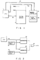
- CPU 1 is a main body of an Intel's i486TM type microprocessor (reference numeral 2 in Fig. 4), for instance, and includes all components except a cache memory and a cache controller.
- System memory 3 generally has a main address space and an extended address space, since it comprises a main memory, which is formed of conventional dynamic RAM's and has the main address space, and an extended memory, which is added to the main memory and has the extended address space.
- Memory controller 4 is connected with CPU 1 by means of control bus 22 and address bus 23, and controls an access of CPU 1 to system memory 3 for both writing and reading based on control signals (a write/read control signal, etc.) and address data both put out of CPU 1.
- Data bus 24 is used to transfer between CPU 1 and system memory 3 those data that have been accessed for writing and reading.
- Memory controller 4 has logic circuit 40 which relates to the gist of the present invention.
- Logic circuit 40 is a determination logic circuit for determining whether or not an address which CPU 1 puts out for an access to system memory 3 exceeds systemic upper limit address value SMAX of a maximal address space of a memory capacity of the computer system, or existent upper limit address value EMAX of a maximal address space of system memory 3 which is actually equipped to the system.
- Systemic upper limit address value SMAX is invariable and is set beforehand for maintaining compatibility of the computer system.
- existent upper limit address value EMAX is variable according to an actually mounted condition of system memory 3.
- existent upper limit address value EMAX can be varied by an addition of an extended memory to the main memory, for instance, and its varying amount or extended address space corresponds to the storage capacity of the extended memory having been added to the main memory.
- Memory controller 4 executes a memory control which validates or invalidates a memory access of CPU 1 based on the determination result of logic circuit 40, and puts out through control buss 22 to CPU 1 a signal which indicates that the memory access is valid or invalid.
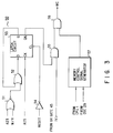
- Logic circuit 40 has registers 41, 42, comparators 43, 44, and OR gate 45, as shown in Fig. 2.
- Register 41 is set with systemic upper limit address value SMAX in advance, whereas register 42 is set with existent upper limit address value EMAX by, for instance, a BIOS (Basic Input and Output System) at a time when the system is activated.
- Comparator 43 compares address AA having been put out of CPU 1 with systemic upper limit address value SMAX having been set to register 41, and puts out a signal having a logic level "H" when address AA from CPU 1 exceeds systemic upper limit address value SMAX.
- Comparator 44 compares address AA from CPU 1 with existent upper limit address value EMAX having been set to register 42, and puts out a signal having a logic level "H” when address AA from CPU 1 exceeds existent upper limit address value EMAX.
- OR gate 45 puts out signal IV instructing invalidation of a memory cycle when it receives the output signal having a logic level "H” from comparator 43 or 44.
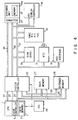
- Fig. 4 is a block diagram showing a structure of a portable computer to which the computer system in the present invention is applied.
- This portable computer comprises 32 bit microcomputer (MPU) 2 such as an Intel's i486TM type microcomputer, system controller 20, and various other units.
- MPU microcomputer
- System controller 20 is an LSI forming an interface between 32 bit MPU 2 and various units belonging to a 16 bit system.
- System controller 20 functions as memory controller 4 which relates to the present invention, a bus controller, an I/O (Input/Output) controller, and so forth.
- System controller 20 is connected with MPU 2 by means of control bus 22, 32 bit address bus 23, and 32 bit data bus 24. Furthermore, system controller 20 is connected with main memory 27 and extended memory 28 by means of memory control bus 25 and memory address bus 26. Note that main memory 27 and extended memory 28 constitute system memory 3 shown in Fig. 1.
- Control bus 22 is used for transfer of various control signals such as signal M/IO (a memory input/output signal), signal W/R (a write/read signal), signal D/C (a data/control signal), signal ADS (an address status signal), signal RDY (a ready signal) which is put out of memory controller 4 within system controller 20, and so forth.
- signal M/IO a memory input/output signal
- signal W/R a write/read signal
- signal D/C a data/control signal
- signal ADS an address status signal
- signal RDY a ready signal
- Memory control bus 25 is used for transfer of memory control signals such as signal RAS (a row address strobe signal) and signal CAS (a column address strobe signal) both put out of memory controller 4.
- RAS a row address strobe signal
- CAS a column address strobe signal
- System controller 20 and MPU 2 are supplied with clock pulse CLK which is necessary for their operation and is generated from clock generating circuit (OCS) 29.
- CLK clock generating circuit
- ROM read-only memory
- RTC real time controller
- HDD hard disk drive
- unit 33 in which a DMAC (a direct memory access controller), a PIC (a programmable interrupt controller), a PIT (a programmable interval timer) and a FDC (a floppy disk controller) are included
- unit 34 in which a KBC (a keyboard controller) and a display controller are included.
- ROM 30 is a BIOS-ROM in which a BIOS is stored.
- System controller 20 is connected with the above listed units 30 - 34 by means of control bus 35, address bus 36 and data bus 37.
- System controller 20 is connected with extension unit 10, which has extended memory 10a inside of it, by means of connector 21 for exclusive use of the extension unit.
- System controller 20 exchanges data, addresses, and various control signals with extended memory 10a mounted in extension unit 10 by means of control bus 35, address bus 36 and data bus 37.
- CPU 1 puts out signal ADS, signal M/IO, signal W/R and signal D/C through control bus 22 to memory controller 4 (system controller 20) in synchronism with clock pulse CLK.
- a symbol "#" shown in Fig. 5 indicates a negative logic.
- Signal M/IO is in a logic level "H” which indicates that an access target is a memory.
- Signal W/R is in a logic level “L” which indicates a read access.
- Signal D/C is in a logic level "H” which indicates data.
- CPU 1 puts out through address bus 23 an address data indicating an address of system memory 3 which is an access target.
- Memory controller 4 converts the address data having been put out of CPU 1 into a combination of a row address and a column address for system memory 3, and supplies them to system memory 3 in synchronism with signal RAS and signal CAS, respectively.
- memory controller 4 executes a memory access validation/invalidation determining process, as shown in the flow chart of Fig. 6.
- systemic upper limit address value SMAX which is a maximal address value of a maximal memory space of the computer system, including a maximally extended address space, is set to register 41.
- Systemic upper limit address value SMAX is an invariable value which is set when the computer system is designed.
- EMAX of a maximal address space of system memory 3 actually mounted on the computer system is set to register 42 by the BIOS having been stored in BIOS-RAM 30 at a time of system excitation (Step S1).
- system memory 3 has such an address space that is constituted by adding to the address apace of main memory 27 an extended address space which corresponds to the memory capacity of extended memory 28.
- an initialization routine stored in the BIOS is executed to perform a system initialization operation. While the system initialization operation is being executed, existent upper limit address value EMAX is set to register 42.
- CPU 1 puts out address AA of an access target in order to access system memory 3 (a read access, in this case) (Step S2).
- Comparator 43 compares address AA having been put out of CPU 1 with systemic upper limit address value SMAX having been set to register 41 (Step S3).
- Comparator 44 compares address AA from CPU 1 with existent upper limit address value EMAX having been set to register 42 (Step S5).
- Step S8 When the comparison result of comparator 41 shows that address An from CPU 1 exceeds systemic upper limit address value SMAX ("YES" in Step S4), OR gate 45 puts out signal IV having a logic level "H,” which indicates that the memory access of CPU 1 is invalid (Step S8). Based on signal IV having the logic level "H,” memory controller 4 executes an invalidation process for invalidating the memory access of CPU 1 (Step S9). More specifically, memory controller 4 stops an output of signals RAS and CAS, and stops a supply of a row address and a column address of system memory 3 that correspond to address data AA. In addition, memory controller 4 puts out to CPU 1 signal RDY indicating a memory access termination (a doted line in (h) of Fig. 5). Due to this, the memory access of CPU 1 is invalidated and the fact that the memory access of CPU 1 is invalidated is instructed to CPU 1.
- the memory access of CPU 1 can be invalidated when an address of an access target exceeds the maximal address space of the computer system, including a maximally extended address space, upon an access of CPU 1 to system memory 3.
- a memory access of CPU 1 can also be invalidated when an address of the access target exceeds the maximal address space of system memory 3 having been actually mounted to the system.
- Some microprocessors have a function of executing a predetermined initialization routine by executing a Far Jump instruction immediately after the CPU has been reset. What follows is another embodiment in which a CPU having such a function is employed.
- CPU 1 When the Far Jump instruction is executed, CPU 1 generally puts out address value AF which is larger than systemic upper limit address value SMAX of the system.
- Memory controller 4 of system controller 20 converts address AF having been put out of CPU 1 to a predetermined address of BIOS-ROM 30 to access a predetermined memory area of BIOS-ROM 30. In the predetermined memory area of BIOS-ROM 30 a Far Jump instruction and a vector address (an address of a jump target) are stored.
- System controller 20 reads the Far Jump instruction and the vector address out of BIOS-ROM 30 and supplies them to CPU 1.
- CPU 1 jumps to the vector address and executes the predetermined initialization routine stored in the vector address.
- address value AF relative to the Far Jump instruction is larger than systemic upper limit address value SMAX, as stated above, it causes memory controller 4 to put out signal IV having a logic level "H" which indicates invalidation of a memory access of CPU 1. Therefore, the Far Jump instruction will not be executed because memory controller 4 invalidates the memory access of CPU 1.
- logic circuit 50 is provided as shown in Fig. 3 to ignore signal IV having a logic level "H," or an invalidation signal, having been put out of logic circuit 40 and to validate logic circuit 40 after any predetermined function has been finished.
- Logic circuit 50 has NOR gate 51, OR gate 52, latch circuit 53, inverter 54, and AND gates 55 and 56.
- memory controller 4 ignores signal IV having a logic level "H," or an invalidation signal, having been put out of logic circuit 40 and validates, with the help of logic circuit 50, various memory control signals (signal RAS, Signal CAS, etc.) MC having been put out of memory control signal generating circuit 5.
- logic circuit 50 will be explained below with reference to the circuit diagram shown in Fig. 3 and the flow chart shown in Fig. 7.
- CPU 1 puts out address AF which is larger than systemic upper limit address value SMAX of the system in order to execute the Far Jump instruction right after the reset has finished (Step S10).
- Address AF causes address A23 having a logic level "H" among each bit of the address data to be put into NOR gate 51.
- CPU 1 puts out along with address value AF both signal ADS, which has a logic level "L,” and signal W/R, which has a logic level “L” and is a read command.
- NOR gate 51 puts out a signal having a logic level “L” when it receives signal W/R having a logic level “L.”
- the output signal having a logic level “L” from NOR gate 51 is supplied through OR gate 52 to data input terminal D of latch circuit 53.
- Latch circuit 53 is cleared when reset signal RESET for resetting CPU 1 is put into its clear CL, and puts out signal Q having a logic level “L” from its output terminal of a positive phase and signal QN having a logic level “H” from its output terminal of an inverted phase.
- signal ADS changes to have a logic level "H”
- latch circuit 53 holds such an input signal that has a logic level "L” and has been supplied to data input terminal D. Therefore, latch circuit 53 maintains output signal QN having a logic level "H.”
- Logic circuit 40 causes OR gate 45 to put out signal IV having a logic level "H,” or an invalidation signal, since address value AF having been put out of CPU 1 is larger than systemic upper limit address value SMAX of the system.
- AND gate 55 receives both output signal QN and signal IV having a logic level "H,” or an invalidation signal, and puts out a signal having a logic level "H,” since both signals having been supplied to AND gate 55 have a logic level "H.”
- AND gate 56 effectively allows the passage of various memory control signals MC having been supplied from memory control signal generating circuit 57, since the output signal from AND gate 55 has a logic level "H.”
- Step S11 when the Far Jump instruction is executed right after the reset ("YES" in Step S11), signal IV having a logic level "H,” or an invalidation signal, having been put out of logic circuit 40 is ignored (Step S12). Therefore, memory controller 4 maintains the validity of the memory access of CPU 1 with the help of valid various memory control signals MC having been put out of memory control signal generating circuit 57 (Step S13). Therefore, CPU 1 executes the aforementioned Far Jump instruction (Step S14).
- logic circuit 50 the output signal of NOR gate 51 will have a logic level "H” since address A23 becomes to have a logic level “L.” Therefore, output signal QN of latch circuit 53 will have a logic level “L” at a time when signal ADS changes to have a logic level “L.” Latch circuit 53 maintains output signal QN having a logic level "L” at a time when signal ADS changes to have a logic level "H.” As a result, the output signal of AND gate 55 will have a logic level "L.” Namely, logic circuit 50 invalidates various memory control signals MC having been put out of memory control generating circuit 57.
- Memory controller 4 therefore executes an invalidation control for invalidating the memory access of CPU 1 in response to signal IV having a logic level "H,” or an invalidation signal, having been put out of logic circuit 40 (Step S15).
- CPU 1 can ignore signal IV having a logic level "H,” or an invalidation signal, having been put out of logic circuit 40 when CPU 1 puts out an address which exceeds the maximal address value (SMAX) of the system in case of executing a predetermined function such as the Far Jump instruction, for instance. Therefore, any predetermined function, including the Far Jump instruction, can be surely executed, and signal IV having a logic level "H,” or an invalidation signal, having been put out of logic circuit 40 can be validated again after any predetermined function has been executed.
- SMAX maximal address value
Landscapes
- Engineering & Computer Science (AREA)
- Theoretical Computer Science (AREA)
- Computer Security & Cryptography (AREA)
- Physics & Mathematics (AREA)
- General Engineering & Computer Science (AREA)
- General Physics & Mathematics (AREA)
- Techniques For Improving Reliability Of Storages (AREA)
- Storage Device Security (AREA)
Applications Claiming Priority (2)
| Application Number | Priority Date | Filing Date | Title |
|---|---|---|---|
| JP3255331A JPH0594376A (ja) | 1991-10-02 | 1991-10-02 | ポータブルコンピユータ |
| JP255331/91 | 1991-10-02 |
Publications (1)
| Publication Number | Publication Date |
|---|---|
| EP0535538A1 true EP0535538A1 (de) | 1993-04-07 |
Family
ID=17277306
Family Applications (1)
| Application Number | Title | Priority Date | Filing Date |
|---|---|---|---|
| EP92116386A Withdrawn EP0535538A1 (de) | 1991-10-02 | 1992-09-24 | Rechnersystem mit Steuereinheit zur Verhinderung des Zugriffs auf nicht-existierende Adressen |
Country Status (2)
| Country | Link |
|---|---|
| EP (1) | EP0535538A1 (de) |
| JP (1) | JPH0594376A (de) |
Cited By (3)
| Publication number | Priority date | Publication date | Assignee | Title |
|---|---|---|---|---|
| EP0658846A1 (de) * | 1993-12-09 | 1995-06-21 | Pitney Bowes Inc. | Adressendekoder mit Speicherzuordnung für ein Mikrokontrollersystem |
| EP0658847A1 (de) * | 1993-12-09 | 1995-06-21 | Pitney Bowes Inc. | Adressendekoder mit Speicherzuordnung und illegaler Adresserkennung für ein Mikrokontrollersystem |
| WO1997027544A1 (en) * | 1996-01-24 | 1997-07-31 | Sun Microsystems, Inc. | Processor with accelerated array access bounds checking |
Citations (4)
| Publication number | Priority date | Publication date | Assignee | Title |
|---|---|---|---|---|
| US3742458A (en) * | 1970-09-30 | 1973-06-26 | Yokogawa Electric Works Ltd | Memory protection system providing fixed, conditional and free memory portions corresponding to ranges of memory address numbers |
| US4787060A (en) * | 1983-03-31 | 1988-11-22 | Honeywell Bull, Inc. | Technique for determining maximum physical memory present in a system and for detecting attempts to access nonexistent memory |
| EP0334523A2 (de) * | 1988-03-18 | 1989-09-27 | Fujitsu Limited | Mikroprozessor |
| EP0440445A2 (de) * | 1990-01-31 | 1991-08-07 | Hewlett-Packard Company | Systemspeicherinitialisierung mit Anwesenheitserkennungskodierung |
-
1991
- 1991-10-02 JP JP3255331A patent/JPH0594376A/ja active Pending
-
1992
- 1992-09-24 EP EP92116386A patent/EP0535538A1/de not_active Withdrawn
Patent Citations (4)
| Publication number | Priority date | Publication date | Assignee | Title |
|---|---|---|---|---|
| US3742458A (en) * | 1970-09-30 | 1973-06-26 | Yokogawa Electric Works Ltd | Memory protection system providing fixed, conditional and free memory portions corresponding to ranges of memory address numbers |
| US4787060A (en) * | 1983-03-31 | 1988-11-22 | Honeywell Bull, Inc. | Technique for determining maximum physical memory present in a system and for detecting attempts to access nonexistent memory |
| EP0334523A2 (de) * | 1988-03-18 | 1989-09-27 | Fujitsu Limited | Mikroprozessor |
| EP0440445A2 (de) * | 1990-01-31 | 1991-08-07 | Hewlett-Packard Company | Systemspeicherinitialisierung mit Anwesenheitserkennungskodierung |
Cited By (4)
| Publication number | Priority date | Publication date | Assignee | Title |
|---|---|---|---|---|
| EP0658846A1 (de) * | 1993-12-09 | 1995-06-21 | Pitney Bowes Inc. | Adressendekoder mit Speicherzuordnung für ein Mikrokontrollersystem |
| EP0658847A1 (de) * | 1993-12-09 | 1995-06-21 | Pitney Bowes Inc. | Adressendekoder mit Speicherzuordnung und illegaler Adresserkennung für ein Mikrokontrollersystem |
| US5530840A (en) * | 1993-12-09 | 1996-06-25 | Pitney Bowes Inc. | Address decoder with memory allocation for a micro-controller system |
| WO1997027544A1 (en) * | 1996-01-24 | 1997-07-31 | Sun Microsystems, Inc. | Processor with accelerated array access bounds checking |
Also Published As
| Publication number | Publication date |
|---|---|
| JPH0594376A (ja) | 1993-04-16 |
Similar Documents
| Publication | Publication Date | Title |
|---|---|---|
| US4388695A (en) | Hardware memory write lock circuit | |
| US5455927A (en) | Dual socket upgradeable computer motherboard with automatic detection and enablement of inserted upgrade CPU chip | |
| US5483646A (en) | Memory access control method and system for realizing the same | |
| US5991858A (en) | Multi-user data processing system with storage protection | |
| KR0138697B1 (ko) | 마이크로컴퓨터 | |
| JPS5963100A (ja) | マイクロプロセツサのためのメモリ管理装置 | |
| US4731740A (en) | Translation lookaside buffer control system in computer or virtual memory control scheme | |
| EP0979460A1 (de) | System zur zugriffskontrolle zu einem register aufgenommen im addressenbereich eines rechnersystems | |
| US6775734B2 (en) | Memory access using system management interrupt and associated computer system | |
| US5544344A (en) | Apparatus for caching smram in an intel processor based computer system employing system management mode | |
| EP0109504A2 (de) | Datensicherungssystem für Speicher- und Ein/Ausgabeeinrichtungen und dergleichen | |
| EP0676687A2 (de) | Stromverwaltungseinheiten für Rechnersysteme | |
| US5057999A (en) | Microprocessor having a protection circuit to insure proper instruction fetching | |
| US5751998A (en) | Memory accessing system with portions of memory being selectively write protectable and relocatable based on predefined register bits and memory selection RAM outputs | |
| US5101486A (en) | Processor having a stackpointer address provided in accordance with connection mode signal | |
| US6938107B2 (en) | Microprocessor preventing erroneous writing to control register | |
| US4628450A (en) | Data processing system having a local memory which does not use a directory device with distributed resident programs and a method therefor | |
| JP3505231B2 (ja) | コンピュータシステム | |
| US5692154A (en) | Circuit for masking a dirty status indication provided by a cache dirty memory under certain conditions so that a cache memory controller properly controls a cache tag memory | |
| CA2028551A1 (en) | Data destination facility | |
| EP0535537A2 (de) | Rechneranordnung mit Cachespeicher | |
| EP0598570A2 (de) | Adressbereichkonfigurationsystem und Verfahren zur Steuerung von Speichersystemoperationen mittels Adressbereichen | |
| JPH0594376A (ja) | ポータブルコンピユータ | |
| EP0350917A2 (de) | Zur Verhinderung des Konkurrenzbetriebs im Speicheradressraum geeignete Personalcomputer-Anordnung | |
| JPS6250863B2 (de) |
Legal Events
| Date | Code | Title | Description |
|---|---|---|---|
| PUAI | Public reference made under article 153(3) epc to a published international application that has entered the european phase |
Free format text: ORIGINAL CODE: 0009012 |
|
| 17P | Request for examination filed |
Effective date: 19921021 |
|
| AK | Designated contracting states |
Kind code of ref document: A1 Designated state(s): DE FR GB |
|
| 18W | Application withdrawn |
Withdrawal date: 19951103 |