EP0535709A2 - Fotoelektrische Halbleiter integrierte Schaltung - Google Patents
Fotoelektrische Halbleiter integrierte Schaltung Download PDFInfo
- Publication number
- EP0535709A2 EP0535709A2 EP92116936A EP92116936A EP0535709A2 EP 0535709 A2 EP0535709 A2 EP 0535709A2 EP 92116936 A EP92116936 A EP 92116936A EP 92116936 A EP92116936 A EP 92116936A EP 0535709 A2 EP0535709 A2 EP 0535709A2
- Authority
- EP
- European Patent Office
- Prior art keywords
- output
- amplifier
- transistor
- opto
- integrated circuit
- Prior art date
- Legal status (The legal status is an assumption and is not a legal conclusion. Google has not performed a legal analysis and makes no representation as to the accuracy of the status listed.)
- Withdrawn
Links
Images


Classifications
-
- H—ELECTRICITY
- H03—ELECTRONIC CIRCUITRY
- H03F—AMPLIFIERS
- H03F3/00—Amplifiers with only discharge tubes or only semiconductor devices as amplifying elements
-
- H—ELECTRICITY
- H04—ELECTRIC COMMUNICATION TECHNIQUE
- H04B—TRANSMISSION
- H04B10/00—Transmission systems employing electromagnetic waves other than radio-waves, e.g. infrared, visible or ultraviolet light, or employing corpuscular radiation, e.g. quantum communication
- H04B10/60—Receivers
- H04B10/66—Non-coherent receivers, e.g. using direct detection
- H04B10/69—Electrical arrangements in the receiver
- H04B10/693—Arrangements for optimizing the preamplifier in the receiver
Definitions
- the present invention relates to an photo-electronic integrated circuit device having a photo-emis- sion/detection element and an electric element and used in a photo-detector of optical fiber communication.
- OEIC photo-electronic integrated circuit device
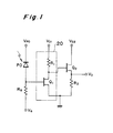
- Fig. 1 An example of a prior art photo-electronic integrated circuit device (OEIC) is shown in Fig. 1.
- the OEIC is monolithically formed on one semiconductor substrate and comprises a photo-diode PD, resistor RG, R1 and R2, and high electron mobility transistor (HEMT) Q1 and Q2.
- the photo-diode PD and the resistor RG constitute a photo-detector stage
- the resistor R1 and the transistor Q1 constitute an amplifier stage
- the transistor Q2 and the resistor R2 constitute a source follower stage.
- the amplifier stage which amplifies the output signal of the photo-diode PD has a very high sensitivity. Accordingly, when an electrical noise signal is externally applied, a final stage of the amplifier stage is significantly affected by the noise.
- the transistor Q1 and the load resistor R1 in the amplifier stage constitute an inverting amplifier 20.
- the inverting amplifier 20 In order for the inverting amplifier 20 to have a unity gain, it is designed such that a product of a conductance of the transistor Q1 and the load resistor R1 is unity.
- a voltage of higher than 4 volts is applied across the source and the drain of the transistor Q1 assuming that a power supply voltage VD1 is 5 volts. Since this voltage essentially corresponds to a breakdown voltage between the source and the drain of the transistor Q1, it causes a problem of likelihood of the breakdown of the transistor.
- the photo-electronic integrated circuit device of the present invention comprises: first and second output terminals for supplying first and second output signals of opposite polarities to an external differential input logic circuit; a photo-detecting device for converting an input light signal to an electrical signal; a first amplifier for amplifying the electrical signal of said photo-detecting device and outputting the same from said first output terminal as said first output signal; and a second amplifier for amplifying the output of said first amplifier and outputting said second output signal having the opposite phase to that of said first output signal, from said second output terminal.
- the photo-electronic integrated circuit device may be monolithically formed on an InP substrate, output buffers may be provided at outputs of the first and second amplifiers, or the output buffers may be source followers including constant current circuits.
- a level shift circuit may be provided in the output of the first amplifier for shifting a voltage level of the output of said first amplifier to output said first output signal and the output to said second amplifiers.
- the first amplifier may include a signal amplifying transistor and a constant current circuit as a load to said transistor, and the transistor may be one of J-FET, HEMT, MISFET and MESFET.
- the second amplifier may include a signal amplifying transistor and a device having a predetermined voltage drop and connected to at least one of a drain or a collector, and a source or an emitter of said transistor, and the device having the predetermined voltage drop may include a plurality of series-connected diodes, or a plurality of diodes and a resistor connected in series.
- the OEIC produces the opposite output at its two output terminals.
- the output of the amplifier of the OEIC is applied to the first output terminal in the same phase.
- the output of the amplifier is also applied to the second output terminal but with the inverted phase through the inverting amplifier.
- the noise When a noise is externally applied, the noise appears in the output signals at the first and second output terminals in the same phase.
- the differential input logic circuit for example such as an ECL, is connected in the rear stage of the OEIC, and a difference between the two output signals appearing at the first and second output terminals is amplified by the differential amplifier. Since the noises included in the output signals appear in the same phase, that is, they are common mode noises, the noises are eliminated by differentiating the output signals at the first and second output terminals. Accordingly, the photo-de- tectorwhich is not substantially affected by the external electrical signal noise is attained.
- the output of the amplifier is applied to the first output terminal in the same phase, and the output of the amplifier is inverted by the inverting amplifier and it is applied to the second output terminal.
- the differential input logic circuit having the differential amplifier input stage which differentiates the two output signals appearing at the first and second output terminals is connected in the rear stage of the OEIC so that the noise components are eliminated by the differential amplifier and the photo-detector which is not affected by the external noise is attained.
- the voltage applied to the transistor may be rendered smaller than the power supply voltage by the voltage drop across the element, and the voltage applied between the drain (collector) and the source (emitter) of the transistor can be reduced.
- a predetermined voltage drop function for example, a level shifting diode or a resistor
- the level shifting means is connected to at least one of the drain (collector) and the source (emitter) of the transistor of the inverting amplifier, the voltage applied between the source and the drain or between the emitter and the collector of the transistor is reduced.
- the inverting amplifier having the unity gain is constructed by the transistor, the break-down in the transistor is prevented.
- Fig. 2 shows a basic configuration of the OEIC in accordance with a first embodiment of the present invention.
- the OEIC of the present embodiment basically comprises a photo-diode PD, an amplifier 1, an output buffer 3, an inverting amplifier 4 and an output buffer 5, which are monolithically formed on an InP substrate.
- the photo-diode PD converts an input light signal to an electrical signal, and the amplifier 1 amplifies the electrical signal detected by the photo-diode PD.
- the inverting amplifier4 is supplied with the output of the amplifier 1, and inverts itwith unity gain.
- the output buffers 3 and 5 prevent the affect by the connection of a circuit to a succeeding stage from appearing in a preceding stage.
- the output buffer 3 is supplied with the output of the amplifier 1 and produces an output signal of the same phase at an output terminal 6.
- the output buffer 5 is supplied with the output of the inverting amplifier 4 and produces an output signal of the opposite phase at an output terminal 7.
- Adifferential input logic circuit is connected to the output terminals 6 and 7.
- Fig. 3 and 4 shows examples of the logic circuit. It is essential that the input stage is constructed by a differential amplifier.
- Fig. 3A shows a differential input buffer which has a transfer characteristic as shown in Fig. 3B and produces outputs Vo and Vo based on inputs D and D of the opposite phases.
- Fig. 4 shows a differential input AND circuit which ANDs complementary inputs A and A and complementary inputs B and B to produce complementary output OUT and OUT .
- Fig. 5 shows a specific circuit configuration of the OEIC having the basic configuration described above and comprises the respective blocks of Fig. 2, that is, the photo-diode PD, the amplifier 1, the level shift circuit 2, the output buffer 3, the inverting amplifier 4 and the output buffer 5.
- the level shift circuit 2 shifts a DC level of the output of the amplifier 1 to a predetermined bias level.
- the output of the level shift circuit 1 is applied to the output buffer 3 and the inverting amplifier 4.
- the amplifier 1 comprises a load by a constant current circuit including a transistor Q1 and a resistor R1, a transistor Q2 which receives the detection signal of the photo-diode PD and amplifies it, and level shifting diodes D1 -D3, which are connected in series between a power supply voltage V DD and ground.
- the level shift circuit 2 comprises a transistor Q3, level shifting diodes D4 -D6, and a load by a constant current circuit including a transistor Q4 and a resistor R2, which are connected in series between the power supply voltage VDD and the ground.
- a gate of the transistor Q3 is connected to a drain of the transistor Q2 of the preceding stage.
- the output buffer 3 comprises a transistor Q5, level shifting diodes D7 -D9, and a load by a constant current circuit including a transistor Q6 and a resistor R3, which are connected in series between the power supply voltage VDD and the ground.
- a source of the transistor Q3 of the preceding stage is connected to a gate of the transistor Q5.
- the inverting amplifier 4 comprises a resistor R4 and a transistor Q7 which are connected in series between the power supply voltage VDD and the ground.
- a gate of the transistor Q7 is connected to a drain of the transistor Q4 of the preceding stage.
- a voltage having the DC level thereof shifted by the level shifting diodes D4-D6 of the preceding stage is applied to the transistor Q7.
- the output buffer 5 comprises a transistor Q8, level shifting diodes D10-D12, and a load by a constant current circuit including a transistor Q9 and a resistor R5, which are connected in series between the power supply voltage VDD and the ground.
- a gate of the transistor Q8 is connected to a drain of the transistor Q7 of the preceding stage.
- the transistor Q8 operates in response to the output signal of the inverting amplifier 4 of the preceding stage.
- the output of the output buffers 3 and 5 are produced at the output terminals 6 and 7 connected to the sources of the transistors Q5 and Q8 of the respective buffers.
- An MSM or PIN photo-diode is used as the photo-diode PD of the OEIC, and junction type field effect transistors (FET's), HEMT's, MISFET's or MESFET's are used as the transistor Q1 -Q9.
- the photo-diode PD is used for an application to light communication in a wavelength band of 1.3-1.6 f..lm and it can detect a light shorter than 1.6 ⁇ m. It uses Inp for an n-layer and GalnAs as a p-layer, and a photo-sensing layer of artificial grating GaInAs having a multi-layer periodic structure is sandwitched between the n-layer and the p-layer.
- the detection signal by the photo-diode PD is amplified by the amplifier 1.
- the amplified signal is applied to the output terminal 6 through the output buffer 3 in the same phase, and the other output of the amplifier 1 is applied to the inverting amplifier 4.
- the phase is inverted thereby, and the resulting output is applied to the output terminal 7 through the output buffer 5.
- the noise appears in the output signals at the two output terminals in the same phase because the circuit is on one chip, and they change in the same manner as the output signals do. That is, the noises are common mode noises. Since a difference between the output signal levels is always substantially constant without regard to the noise, it is eliminated by the differential input logic circuit connected to the output terminals 6 and 7.
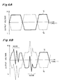
- Fig. 6A shows waveforms when no external noise is applied.
- the light signal is applied to the photo-diode PD of the OEIC and a signal waveform V1 shown by a solid line is produced at the output terminal 6.
- Asignal waveform V2 having the inverted phase as shown by a broken line is produced at the other output terminal 7 because the inverting amplifier 4 is connected in the preceding stage.
- the noise appears at the output terminals 6 and 7 as the common mode noise as shown in Fig. 6 (b) so that the output signals from these terminals are changed in the same manner. That is, the outputs appearing at the output terminals 6 and 7 have waveforms consisting of signal components of the opposite phases and noise components of the same phase.
- the logic circuit having the differential amplifier in the input stage thereof as shown in Figs. 3 and 4 is connected to the rear stage of the OEIC.
- the logic circuit performs a predetermined logic arithmetic on the basis of a difference V1-V2 between the two signals appearing at the output terminals 6 and 7. As a result, the noise components are cancelled out as shown in Fig. 7 so that the electrical signal free of the noise component is produced.
- the OEIC circuit is shown in Fig. 5 although the present invention is not limited to the specific circuit configuration but it may be a conventional OEICwith the addition of an inverting amplifier for inverting the output of the amplifier and the output terminal to which the output of the inverting amplifier is applied.
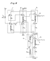
- Fig. 8 shows a circuit diagram of the OEIC in accordance with the second embodiment of t he present invention.
- the OEIC is monolithically formed on an InP substrate as it is in the first embodiment, and comprises a photo-diode PD for converting an input light signal to an electrical signal, an amplifier 1 for amplifying the electrical signal detected by the photo-diode PD, a level shift circuit 2 for shifting a DC level of the output of the amplifier 1, an output buffer 3 to which the output of the level shift circuit 2 is applied, a unity gain inverting amplifier4 for inverting the output of the level shift circuit 2, and an output buffer 5 to which the output of the inverting amplifier 4 is applied.
- a differential input logic circuit is connected to output terminals 6 and 7 as it is in the first embodiment shown in Fig. 3 and 4. The respective blocks are explained below.
- the amplifier 1 comprises a load by a constant current circuit including a transistor Q1 and a resistor R1, a transistor Q2 for amplifying the detection signal of the photo-diode PD, and level shifting diodes Dl-D3, which are connected in series between a power supply voltage VDD and ground.
- the level shift circuit 2 comprises a transistor Q3, level shifting diodes D4 -D6, and a load by a constant current circuit including a transistor Q4 and a resistor R2, which are connected in series between the power supply voltage VDD and the ground.
- a gate of the transistor Q3 is connected to a gate of the transistor Q1 of the preceding stage.
- the output buffer 3 comprises a transistor Q5 level shifting diodes D7 -D9, and a load by a constant current circuit including a transistor Q6 and a resistor R3, which are connected in series between the power supply voltage VDD and the ground.
- a source of the transistor Q3 of the preceding stage is connected to a gate of the transistor Q5.
- the inverting amplifier4 comprises level shifting diodes D13 and D14, a resistor R4, a transistor Q7 and level shifting diodes D15 ⁇ D17, which are connected in series between the power supply voltage VDD and the ground.
- a gate of the transistor Q7 is connected to a drain of the transistor Q4 of the preceding stage, and a voltage having a DC level thereof shifted by the level shifting diodes D4-D6 of the preceding stage is applied to the gate of the transistor Q7.
- the output buffer 5 comprises a transistor Q8, level shifting diodes D10 ⁇ D12, and a load by a constant current circuit including a transistor Q9 and a resistor R5, which are connected in series between the power supply voltage VDD and the ground.
- a gate of the transistor Q8 is connected to a drain of the transistor Q7 of the preceding stage, and the transistor Q8 operates in response to the output signal of the inverting amplifier 4 of the preceding stage.
- the outputs of the output buffers 3 and 5 are produced at the output terminals 6 and 7 connected to the sources of the transistors Q5 and Q8 of the respective buffers.
- An MSM or PIN photo-diode is used as the photo-diode PD of the OEIC, and junction type field effect transistors (FET's), HEMT's, MISFET's or MESFET's are used as the transistors Q1 -Q9.
- the photo-diode PD is used for an application to light communication in a wavelength band of 1.3 ⁇ 1.6 ⁇ m, and it detects a light shorter than 1.6 ⁇ m.
- InP is used for the n-layer, and a photo-sensing layer of artificial grating GalnAs having a multi-layer periodic structure is sandwiched between the n-layer and the p-layer.
- Fig. 9 shows a specific pattern used when the OEIC of Fig. 8 is formed on the InP substrate.
- Fig. 10 shows an arrangement of the elements of the OEIC.
- THE photo-diode is arranged substantially at the center of the chip and pads are connected to pins of a package.
- the operation of the present embodiment is similar to that of the first embodiment.
- the noise appears as common mode noises because the circuit is on one chip. Since a difference between the output signal levels is always substantially constant without regard to the noise, it is eliminated by the differential input logic circuit connected to the output terminals 6 and 7.
- a gain of the inverting amplifier 4 is determined by a product of a trans-conductance of the transistor Q7 and the resistor (load resistor) R4. Assuming that the trans-conductance of the transistor Q7 is approximately 6 ms and the resistance of the resistor R4 is approximately 155 ohm, the gain of the inverting amplifier 4 is approximately unity.
- the diodes D13 ⁇ D17 provide voltage drop of approximately 0.6 volt per diode. Accordingly, when two diodes are connected in series, the voltage drop is approximately 1.2 volt, and when three diodes are connected in series, the voltage drop is approximately 1.8 volt.
- the inverting amplifier 4 shown in Fig. 8 the three series-connected diodes D15, D16 and Dl 7 are inserted between the source of the transistor Q7 and the ground, and the two series-connected diodes D13 and D14 are inserted between the resistor R4 and the 5-volts power supply voltage VDD so that the total voltage drop is 3 volts. As a result, the voltage of 2 volts is applied across the transistor Q7 and the resistor R4.
- a current flowing through the transistor Q7 is approximately 3 mA, and the voltage drop in the resistor R4 is approximately 0.5 volt.
- a voltage applied between the source and the drain of the transistor Q7 is approximately 1.5 volt which is far below a breakdown voltage between the source and the drain of the transistor Q7, and the voltage breakdown of the transistor Q7 is prevented.
- the three diodes are series-connected to the drain of the transistor Q7 of the inverting amplifier 4 and the two diodes are series-connected to the source.
- diodes or resistors may be connected to at least one of the source and the drain.
- the inverting amplifier is constructed by field effect transistors.
- the configuration of the present embodiment may also be applied to attain the same effects and advantages.
- Fig. 11 shows a configuration by bipolar transistors in which the respective blocks are similar to those of the previous embodiments.
Landscapes
- Engineering & Computer Science (AREA)
- Physics & Mathematics (AREA)
- Electromagnetism (AREA)
- Computer Networks & Wireless Communication (AREA)
- Signal Processing (AREA)
- Power Engineering (AREA)
- Amplifiers (AREA)
Applications Claiming Priority (4)
| Application Number | Priority Date | Filing Date | Title |
|---|---|---|---|
| JP25780291A JP3198482B2 (ja) | 1991-10-04 | 1991-10-04 | 光電子回路素子 |
| JP25780991A JP3198483B2 (ja) | 1991-10-04 | 1991-10-04 | 光電子回路素子 |
| JP257809/91 | 1991-10-04 | ||
| JP257802/91 | 1991-10-04 |
Publications (2)
| Publication Number | Publication Date |
|---|---|
| EP0535709A2 true EP0535709A2 (de) | 1993-04-07 |
| EP0535709A3 EP0535709A3 (en) | 1994-06-01 |
Family
ID=26543401
Family Applications (1)
| Application Number | Title | Priority Date | Filing Date |
|---|---|---|---|
| EP19920116936 Withdrawn EP0535709A3 (en) | 1991-10-04 | 1992-10-03 | Photo-electric integrated circuit device |
Country Status (3)
| Country | Link |
|---|---|
| US (1) | US5250800A (de) |
| EP (1) | EP0535709A3 (de) |
| KR (1) | KR960006632B1 (de) |
Cited By (1)
| Publication number | Priority date | Publication date | Assignee | Title |
|---|---|---|---|---|
| CN103036424A (zh) * | 2011-09-29 | 2013-04-10 | 东芝照明技术株式会社 | 集成化开关电源装置及电气设备 |
Families Citing this family (2)
| Publication number | Priority date | Publication date | Assignee | Title |
|---|---|---|---|---|
| US6307759B1 (en) | 1997-10-31 | 2001-10-23 | Hitachi, Ltd. | Control device for electric power translating device |
| CA2312516C (en) * | 2000-06-27 | 2004-03-02 | Ibm Canada Limited-Ibm Canada Limitee | Infrared transceiver with isolated analog output |
Family Cites Families (3)
| Publication number | Priority date | Publication date | Assignee | Title |
|---|---|---|---|---|
| JPH0287709A (ja) * | 1988-09-26 | 1990-03-28 | Hitachi Ltd | 光受信回路 |
| US5025456A (en) * | 1989-02-02 | 1991-06-18 | At&T Bell Laboratories | Burst mode digital data receiver |
| US5073717A (en) * | 1990-10-15 | 1991-12-17 | The United States Of America As Represented By The Secretary Of The Army | Optical control of a microwave switch |
-
1992
- 1992-09-30 US US07/953,804 patent/US5250800A/en not_active Expired - Lifetime
- 1992-10-02 KR KR1019920018110A patent/KR960006632B1/ko not_active Expired - Lifetime
- 1992-10-03 EP EP19920116936 patent/EP0535709A3/en not_active Withdrawn
Cited By (1)
| Publication number | Priority date | Publication date | Assignee | Title |
|---|---|---|---|---|
| CN103036424A (zh) * | 2011-09-29 | 2013-04-10 | 东芝照明技术株式会社 | 集成化开关电源装置及电气设备 |
Also Published As
| Publication number | Publication date |
|---|---|
| EP0535709A3 (en) | 1994-06-01 |
| KR930009231A (ko) | 1993-05-22 |
| US5250800A (en) | 1993-10-05 |
| KR960006632B1 (ko) | 1996-05-22 |
Similar Documents
| Publication | Publication Date | Title |
|---|---|---|
| US5329115A (en) | Optical receiver circuit | |
| EP1011194B1 (de) | Schneller optoelektronischer Differenz-Empfänger | |
| JP2957100B2 (ja) | 光受信器装置 | |
| JPS634727A (ja) | 光学的デジタル信号用受信装置 | |
| US4902982A (en) | Nonlinear noninverting transimpedance amplifier | |
| US5250800A (en) | Photo-electric integrated circuit device with opposite phase amplifiers into logic circuitry | |
| DE59308096D1 (de) | Integrierte Halbleiterschaltungsanordnung | |
| US6175438B1 (en) | Differential optical signal receiver | |
| US4817208A (en) | Fiber optic receiver | |
| US6005240A (en) | Triggered receivers for optoelectronic-VLSI circuits | |
| US5349287A (en) | Low power comparator having a non-saturating current mirror load | |
| EP0525807A2 (de) | Optoelektronische integrierte Schaltung | |
| US6919550B2 (en) | Detector for short wave fiber optic communications with compensation to reduce detector jitter | |
| JP3198482B2 (ja) | 光電子回路素子 | |
| JP3106435B2 (ja) | 光電子集積回路 | |
| JP3106436B2 (ja) | 光電子集積回路 | |
| JP3198483B2 (ja) | 光電子回路素子 | |
| JP2001168374A (ja) | 光電気変換回路 | |
| RU2058661C1 (ru) | Усилитель фототока | |
| JP3106434B2 (ja) | 光電子集積回路 | |
| JPH0779122A (ja) | 増幅回路 | |
| SU1084967A1 (ru) | Эмиттерный повторитель | |
| JPS6315519A (ja) | インタ−フエイス回路 | |
| JPS59198032A (ja) | 光受信回路 | |
| JPH05203681A (ja) | 半導体センサ |
Legal Events
| Date | Code | Title | Description |
|---|---|---|---|
| PUAI | Public reference made under article 153(3) epc to a published international application that has entered the european phase |
Free format text: ORIGINAL CODE: 0009012 |
|
| AK | Designated contracting states |
Kind code of ref document: A2 Designated state(s): DE FR GB |
|
| PUAL | Search report despatched |
Free format text: ORIGINAL CODE: 0009013 |
|
| AK | Designated contracting states |
Kind code of ref document: A3 Designated state(s): DE FR GB |
|
| 17P | Request for examination filed |
Effective date: 19941201 |
|
| 17Q | First examination report despatched |
Effective date: 19950921 |
|
| 18W | Application withdrawn |
Withdrawal date: 19960717 |