EP0536152B1 - Monolithisch integrierte halbleiteranordnung mit einer deckelektrode - Google Patents
Monolithisch integrierte halbleiteranordnung mit einer deckelektrode Download PDFInfo
- Publication number
- EP0536152B1 EP0536152B1 EP91909456A EP91909456A EP0536152B1 EP 0536152 B1 EP0536152 B1 EP 0536152B1 EP 91909456 A EP91909456 A EP 91909456A EP 91909456 A EP91909456 A EP 91909456A EP 0536152 B1 EP0536152 B1 EP 0536152B1
- Authority
- EP
- European Patent Office
- Prior art keywords
- zone
- substrate
- main surface
- monolithically integrated
- region
- Prior art date
- Legal status (The legal status is an assumption and is not a legal conclusion. Google has not performed a legal analysis and makes no representation as to the accuracy of the status listed.)
- Expired - Lifetime
Links
- 239000004065 semiconductor Substances 0.000 title claims abstract description 21
- 239000000758 substrate Substances 0.000 claims abstract description 30
- 238000002161 passivation Methods 0.000 claims abstract description 4
- 230000015556 catabolic process Effects 0.000 abstract description 17
- 239000011248 coating agent Substances 0.000 abstract 1
- 238000000576 coating method Methods 0.000 abstract 1
- 239000002184 metal Substances 0.000 abstract 1
- XUIMIQQOPSSXEZ-UHFFFAOYSA-N Silicon Chemical compound [Si] XUIMIQQOPSSXEZ-UHFFFAOYSA-N 0.000 description 4
- 229910052710 silicon Inorganic materials 0.000 description 4
- 239000010703 silicon Substances 0.000 description 4
- 230000000903 blocking effect Effects 0.000 description 3
- 238000010586 diagram Methods 0.000 description 3
- 238000009792 diffusion process Methods 0.000 description 3
- 230000010354 integration Effects 0.000 description 2
- 230000007613 environmental effect Effects 0.000 description 1
- 238000004519 manufacturing process Methods 0.000 description 1
- 239000007858 starting material Substances 0.000 description 1
Images


Classifications
-
- H—ELECTRICITY
- H10—SEMICONDUCTOR DEVICES; ELECTRIC SOLID-STATE DEVICES NOT OTHERWISE PROVIDED FOR
- H10D—INORGANIC ELECTRIC SEMICONDUCTOR DEVICES
- H10D30/00—Field-effect transistors [FET]
- H10D30/60—Insulated-gate field-effect transistors [IGFET]
- H10D30/64—Double-diffused metal-oxide semiconductor [DMOS] FETs
- H10D30/66—Vertical DMOS [VDMOS] FETs
- H10D30/668—Vertical DMOS [VDMOS] FETs having trench gate electrodes, e.g. UMOS transistors
-
- H—ELECTRICITY
- H10—SEMICONDUCTOR DEVICES; ELECTRIC SOLID-STATE DEVICES NOT OTHERWISE PROVIDED FOR
- H10D—INORGANIC ELECTRIC SEMICONDUCTOR DEVICES
- H10D62/00—Semiconductor bodies, or regions thereof, of devices having potential barriers
- H10D62/10—Shapes, relative sizes or dispositions of the regions of the semiconductor bodies; Shapes of the semiconductor bodies
- H10D62/102—Constructional design considerations for preventing surface leakage or controlling electric field concentration
- H10D62/103—Constructional design considerations for preventing surface leakage or controlling electric field concentration for increasing or controlling the breakdown voltage of reverse-biased devices
- H10D62/105—Constructional design considerations for preventing surface leakage or controlling electric field concentration for increasing or controlling the breakdown voltage of reverse-biased devices by having particular doping profiles, shapes or arrangements of PN junctions; by having supplementary regions, e.g. junction termination extension [JTE]
-
- H—ELECTRICITY
- H10—SEMICONDUCTOR DEVICES; ELECTRIC SOLID-STATE DEVICES NOT OTHERWISE PROVIDED FOR
- H10D—INORGANIC ELECTRIC SEMICONDUCTOR DEVICES
- H10D64/00—Electrodes of devices having potential barriers
- H10D64/111—Field plates
Definitions
- the invention relates to a monolithically integrated semiconductor arrangement according to the preamble of claim 1.
- a substrate has a weak doping under a first main surface (substrate region n ⁇ ) and a high doping of the same conductivity type under a second main surface, at least in the finished arrangement ( Substrate area n+).
- a first zone (p), which forms a pn junction with the substrate, and a second zone (n+) of the same conductivity type as the substrate, but which does not touch the first zone (p), are diffused in from the first main surface.
- the first main surface of the substrate is covered by an insulating passivation layer.
- a metallic cover electrode lies over this layer and covers substrate areas (substrate area n ⁇ ) bordering the first main surface, the edge areas of the first zone (p) and the edge areas of the second zone (n+).
- a protection of a planar transistor arrangement against environmental influences, possibly combined with an influence on the breakdown voltage, is achieved here by the metallic cover electrode lying above the space charge region.
- the cover electrode lies at a potential between the base and the collector determined by a voltage divider.
- the breakdown voltage is essentially determined by this potential and the thickness of the oxide under the top electrode.
- FIGS. 1 to 6 are limited to the representation of the base-collector diode of an NPN transistor.
- the base is labeled A (anode) and the collector K (cathode).
- the invention is also suitable for pnp transistors, with p and n doping to be interchanged in each case.
- first main surface 3 substrate region n ⁇
- second main surface 4 substrate area n+
- a first zone (p), which forms a pn junction with the substrate 2 and a second zone (n+) of the same conductivity type as the substrate, are produced in a known manner by means of photo technology, doping and diffusion.
- the first zone (p) and the second zone (n+) do not touch.
- the second zone (n+) can be diffused in simultaneously with the emitter.
- the front side 3 is covered with an insulating passivation layer 5, over which a metallic cover electrode D is arranged.
- the cover electrode D covers the substrate region (substrate region n ⁇ ) bordering the front side 3, the edge regions of the first zone (p) and the edge regions of the second zone (n+).
- connection for the anode A is located on the front side 3 and connected to the first zone (p).
- the connection for the cathode K (collector) is connected on the rear side 4 to the substrate region (n+).
- the second zone (n+) limits the space charge to areas under the top electrode when reverse voltage is applied between the anode A and the cathode K.
- the top electrode D can be connected to a voltage divider formed by resistors R1 and R2 between the anode A and the cathode K.
- U1 is the enrichment breakdown voltage and U2 the depletion breakdown voltage of the MOS structure formed by the cover electrode D, the underlying oxide 5 and the silicon 2.
- the voltage divider R1 / R2 can be monolithically integrated in such a way that the resistor R1 instead of the cathode K with the practically equal potential second zone (n+) on the front 3 is connected. It is also known how the reverse voltage between the anode A and K can be made adjustable, for example by means of Zener diodes in series with the resistors, which are short-circuited if necessary.
- the cover electrode D additionally covers an additional zone (zone ⁇ ) bordering the second zone (n +), the surface concentration of which is lower than that of the second zone (n+).
- the cover electrode D additionally covers an additional zone (zone ⁇ ) bordering the first zone (p), the surface concentration of which is lower than that of the first zone (p). From US-A-4 074 293 it is known that such a design of a pn junction can lead to a substantially higher breakdown voltage.
- both additional zones (zone ⁇ and zone ⁇ ) are present.
- Both additional zones ⁇ and ⁇ are produced in a known manner by means of photo technology, doping and diffusion.
- FIG. 5 shows an arrangement corresponding to FIG. 2 with an additional zone ⁇ , in which the cover electrode D and the anode A are connected or the cover electrode D is connected to the same potential as the first zone (p).
- the benefit of the additional zone ⁇ can be seen from the diagram according to FIG. 7.
- the depletion breakdown voltage between the anode A and the cathode K is shown, in the case without the additional zone ⁇ (lower curve branch) and with the additional zone ⁇ (upper curve branch).
- the breakdown voltage is plotted upwards and the thickness of the oxide layer under the cover electrode D to the right. It can be seen that depending on the thickness of the oxide layer, significantly higher values for the breakdown voltage are achieved when an additional zone ⁇ is used.
- FIG. 6 shows a semiconductor arrangement corresponding to FIG. 3 with an additional zone ⁇ , the cover electrode D being connected to the cathode K or the cover electrode D and the cathode K being connected to the same potential, a connection also with the second zone (n+) is possible.
- the enrichment breakdown voltage with and without the additional zone ⁇ is shown in FIG. 8 similarly to FIG. 7. It can also be seen from this that, depending on the thickness of the oxide layer under the cover electrode D, significantly higher values for the breakdown voltage are achieved if an additional zone ⁇ is introduced.
- FIGS. 5 and 6 therefore make it possible in certain cases to achieve a desired blocking capability between the anode and the cathode even without the integration of a voltage divider, which takes up the silicon area.
- FIG. 4 An arrangement according to Fig. 4 is useful when a higher blocking ability is desired in connection with a voltage divider R1 / R2.
Landscapes
- Thyristors (AREA)
- Semiconductor Integrated Circuits (AREA)
- Bipolar Transistors (AREA)
- Bipolar Integrated Circuits (AREA)
Abstract
Description
- Die Erfindung betrifft eine monolithisch integrierte Halbleiteranordnung nach dem Oberbegriff des Anspruchs 1.
- Bei einer bekannten, monolithisch integrierten, Halbleiteranordnung (DE-OS 32 27 536) weist ein Substrat unter einer ersten Hauptoberfläche eine schwache Dotierung (Substratbereich n⁻) und unter einer zweiten Hauptoberfläche, mindestens bei der fertigen Anordnung, eine hohe Dotierung des gleichen Leitfähigkeitstyps (Substratbereich n⁺) auf. Von der ersten Hauptoberfläche sind eine erste Zone (p), die mit dem Substrat einen pn-Übergang bildet, und eine zweite Zone (n⁺) vom gleichen Leitfähigkeitstyp wie das Substrat, die aber die erste Zone (p) nicht berührt, eindiffundiert.
- Die erste Hauptoberfläche des Substrats wird mit Ausnahme von Kontaktfenstern von einer isolierenden Passivierungsschicht bedeckt. Über dieser Schicht liegt eine metallische Deckelektrode, die an die erste Hauptoberfläche grenzende Substratgebiete (Substratbereich n⁻), die Randgebiete der ersten Zone (p) und die Randgebiete der zweiten Zone (n⁺) überdeckt.
- Durch die über dem Raumladungsgebiet liegende, metallische Deckelektrode wird hier ein Schutz einer planaren Transistoranordnung gegen Umgebungseinflüsse, gegebenenfalls verbunden mit einer Beeinflussung der Durchbruchspannung erreicht. Die Deckelektrode liegt dazu auf einem durch einen Spannungsteiler bestimmten Potential zwischen Basis und Kollektor. Die Durchbruchspannung wird im wesentlichen durch dieses Potential und die Dicke des Oxids unter der Deckelektrode bestimmt.
- Die Verwendung eines Spannungsteilers ist eine relativ aufwendige Maßnahme, wobei dessen Integration in die Halbleiteranordnung Siliziumfläche beansprucht. Zudem ist es wünschenswert, bei gleicher Oxiddicke eine höhere Durchbruchspannung zu erreichen. Das wird erfindungsgemäß durch eine Ausbildung der Halbleiteranordnung nach dem kennzeichnenden Teil des Anspruchs 1 erreicht.
- Durch Eindiffusion von einer der zweiten Zone (n⁺) zugeordneten, die erste Zone (p) nicht berühenden zusätzlichen Zone (π) die vom gleichen Leitfähigkeitstyp, jedoch mit geringerer Dotierung wie die zweite Zone (n⁺) ist, kann bei gleicher Oxiddicke eine gegenüber der bekannten Halbleiteranordnung höhere Durchbruchspannung erreicht werden. Damit wird es in bestimmten Fällen möglich, auf einen Spannungsteiler zum Anschluß der Deckelektrode zu verzichten und die gewünschte Sperrfähigkeit curch eine Verbindung der Deckelektrode mit der Basis/Anode bzw. Kollektor/Kathode zu erreichen.
- Die Erfindung wird anhand der Zeichnung näher erläutert.
- Es zeigen:
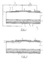
- Fig. 1
- eine monolithisch integrierte Halbleiteranordnung mit einem Spannungsteiler nach dem Stand der Technik,
- Fig. 2
- eine erfindungsgemäße monolithisch integrierte Halbleiteranordnung mit einer zusätzlichen Zone (Zone ν), die einer n⁺-Zone zugeordnet ist,
- Fig. 3
- eine monolithisch integrierte Halbleiteranordnung mit einer zusätzlichen Zone (Zone π), die einer p-Zone zugeordnet ist,
- Fig. 4
- eine erfindungsgemäße Halbleiteranordnung, die beide zusätzlichen Zonen (Zone ν und Zone π) aus den Fig. 2 und 3 enthält,
- Fig. 5
- eine beschaltete Halbleiteranordnung nach Fig. 2,
- Fig. 6
- eine beschaltete Halbleiteranordnung nach Fig. 3,
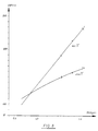
- Fig. 7
- ein Diagramm, das im Vergleich mit dem Stand der Technik den Anstieg der Durchbruchspannung bei Verwendung der zusätzlichen Zone nach Fig. 2 (Zone ν) zeigt und
- Fig. 8
- ein Diagramm, das im Vergleich mit dem Stand der Technik den Anstieg der Durchbruchspannung bei Verwendung der zusätzlichen Zone nach Fig. 3 (Zone π) darstellt.
- Allgemein ist festzustellen, daß die Erfindung bei Transistoren in Planartechnik angewendet werden soll. Da der Emitter dabei keine Rolle spielt, sind die Fig. 1 bis 6 auf die Darstellung der Basis-Kollektor-Diode eines npn-Transistors beschränkt. Die Basis ist dabei mit A (Anode) und der Kollektor mit K (Kathode) bezeichnet.
- Sinngemäß ist die Erfindung auch für pnp-Transistoren geeignet, wobei jeweils p- und n-Dotierung zu vertauschen sind.
- In Fig. 1 ist eine monolithisch integrierte Halbleiteranordnung 1 dargestellt, deren Ausgangsmaterial für die Herstellung ein Silizium-Substrat 2 ist, das auf der Vorderseite (erste Hauptoberfläche 3) schwach (Substratbereich n⁻) und auf der Rückseite (zweite Hauptoberfläche 4) hoch dotiert (Substratbereich n⁺) ist.
- Auf der Vorderseite 3 sind in bekannter Weise mittels Fototechnik, Dotierung und Diffusion eine erste Zone (p), die mit dem Substrat 2 einen pn-Übergang bildet und eine zweite Zone (n⁺) vom gleichen Leitfähigkeitstyp wie das Substrat hergestellt. Die erste Zone (p) und die zweite Zone (n⁺) berühren sich nicht. Die zweite Zone (n⁺) kann gleichzeitig mit dem Emitter eindiffundiert werden.
- Die Vorderseite 3 ist mit Ausnahme von Kontaktfenstern mit einer isolierenden Passivierungsschicht 5 bedeckt, über der eine metallische Deckelektrode D angeordnet ist. Die Deckelektrode D überdeckt das an die Vorderseite 3 grenzende Substratgebiet (Substratbereich n⁻), die Randgebiete der ersten Zone (p) und die Randgebiete der zweiten Zone (n⁺).
- An der Vorderseite 3 und mit der ersten Zone (p) verbunden liegt der Anschluß für die Anode A. Auf der Rückseite 4 mit dem Substratbereich (n⁺) verbunden liegt der Anschluß für die Kathode K (Kollektor). Die zweite Zone (n⁺) begrenzt die Raumladung auf Gebiete unter der Deckelektrode, wenn zwischen der Anode A und der Kathode K Sperrspannung angelegt wird.
- Nach dem Stand der Technik gemäß Fig. 1 kann die Deckelektrode D an einen durch Widerstände R₁ und R₂ gebildeten Spannungsteiler zwischen der Anode A und der Kathode K angeschlossen werden. Die im Falle von R₁ bzw. R₂ = 0 zwischen der Anode A und der Kathode K erreichbaren Durchbruchspannungen sind U₁ bzw. U₂. Dabei ist U₁ die Anreicherungsdurchbruchspannung und U₂ die Verarmungsdurchbruchspannung der durch die Deckelektrode D, das darunterliegende Oxid 5 und das Silizium 2 gebildeten MOS-Struktur. Die maximal erreichbare Durchbruchspannung ist U₁ + U₂, wenn R₁ : R₂ = U₂ : U₁. Aus dem Stand der Technik ist es auch bekannt, wie der Spannungsteiler R₁/R₂ monolithisch integriert werden kann, in der Weise, daß der Widerstand R₁ anstelle mit der Kathode K mit der praktisch auf gleichem Potential liegenden zweiten Zone (n⁺) auf der Vorderseite 3 verbunden wird. Weiter ist es bekannt, wie die Sperrspannung zwischen der Anode A und K abgleichbar gemacht werden kann, beispielsweise durch Zener-Dioden in Reihe zu den Widerständen, die bei Bedarf kurzgeschlossen werden.
- In der erfindungsgemäßen Halbleiteranordnung nach Fig. 2 überdeckt die Deckelektrode D zusätzlich eine an die zweite Zone (n+) grenzende, zusätzliche Zone (Zone ν), deren Oberflächenkonzentration geringer ist als die der zweiten Zone (n⁺).
- In der Halbleiteranordnung nach Fig. 3 überdeckt die Deckelektrode D zusätzlich eine an die erste Zone (p) grenzende, zusätzliche Zone (Zone π), deren Oberflächenkonzentration geringer ist als die der ersten Zone (p). Aus US-A-4 074 293 ist bekannt, daß eine derartige Ausführung eines pn-Übergangs zu einer wesentlich höheren Durchbruchspannung führen kann.
- In der erfindungsgemäßen Halbleiteranordnung nach Fig. 4 sind beide zusätzlichen Zonen (Zone ν und Zone π) vorhanden.
- Beide zusätzlichen Zonen ν und π werden in bekannter Weise mittels Fototechnik, Dotierung und Diffusion hergestellt.
- In Fig. 5 ist eine Anordnung entsprechend der Fig. 2 mit einer zusätzlichen Zone ν dargestellt, bei der die Deckelektrode D und die Anode A verbunden sind bzw. die Deckelektrode D auf das gleiche Potential wie die erste Zone (p) gelegt ist.
- Aus dem Diagramm nach Fig. 7 ist der Nutzen der zusätzlichen Zone ν zu entnehmen. Dabei ist die Verarmungsdurchbruchspannung zwischen der Anode A und der Kathode K eingezeichnet, für den Fall ohne der zusätzlichen Zone ν (unterer Kurvenast) und mit der zusätzlichen Zone ν (oberer Kurvenast). Nach oben ist die Durchbruchspannung aufgetragen und nach rechts die Dicke der Oxidschicht unter der Deckelektrode D. Es ist zu entnehmen, daß je nach der Dicke der Oxidschicht zum Teil deutlich höhere Werte für die Durchbruchspannung erreicht werden, wenn eine zusätzliche Zone ν verwendet wird.
- In Fig. 6 ist eine Halbleiteranordnung entsprechend Fig. 3 mit einer zusätzlichen Zone π dargestellt, wobei die Deckelektrode D mit der Kathode K verbunden ist bzw. die Deckelektrode D und die Kathode K auf das gleiche Potential gelegt werden, wobei auch eine Verbindung mit der zweiten Zone (n⁺) möglich ist.
- In Fig. 8 ist dabei ähnlich wie in Fig. 7 die Anreicherungsdurchbruchspannung mit und ohne der zusätzlichen Zone π eingezeichnet. Auch hieraus ist zu entnehmen, daß je nach Dicke der Oxidschicht unter der Deckelektrode D deutlich höhere Werte für die Durchbruchspannung erreicht werden, wenn eine zusätzliche Zone π eingebracht wird.
- Anordnungen entsprechend den Fig. 5 und 6 machen es daher in bestimmten Fällen möglich, eine gewünschte Sperrfähigkeit zwischen der Anorde und Kathode auch ohne die Siliziumfläche beanspruchende Integration eines Spannungsteilers zu erreichen.
- Eine Anordnung entsprechend der Fig. 4 ist dann nützlich, wenn in Verbindung mit einem Spannungsteiler R₁/R₂ eine höhere Sperrfähigkeit gewünscht wird.
Claims (7)
- Monolithisch integrierte Halbleiteranordnung, bei der in ein Substrat (2), das unter einer ersten Hauptoberfläche (3) eine schwache Dotierung (n⁻) und unter einer zweiten Hauptoberfläche (4) eine hohe Dotierung des gleichen Leitfähigkeitstyps (n⁺) aufweist, von der ersten Hauptoberfläche (3) eine erste Zone (p), die mit dem Substrat (2) einen pn-Übergang bildet, und eine zweite Zone (n⁺) von gleichem Leitfähigkeitstyp wie das Substrat (2), die die erste Zone (p) nicht berührt, eindiffundiert sind und bei der eine die erste Hauptoberfläche (3) des Substrats (2) mit Ausnahme von Kontaktfenstern bedeckende isolierende Passivierungsschicht (5) und eine über dieser Schicht (5) liegende metallische Deckelektrode (D), die an die erste Hauptoberfläche (3) grenzende Substratgebiete (n⁻), Randgebiete der ersten Zone (p) und Randgebiete der zweiten Zone (n⁺) überdeckt, vorgesehen sind, dadurch gekennzeichnet, daß von der ersten Hauptoberfläche (3) eine der zweiten Zone (n⁺) zugeordnete, die erste Zone (p) nicht berührende zusätzliche Zone (ν) eindiffundiert ist, die vom gleichen Leitfähigkeitstyp, jedoch mit geringerer Dotierung wie die zweite Zone (n⁺) ist, die unterhalb der zweiten Zone (n⁺) liegt und deren Randgebiet im Bereich der Deckelektrode (D) umfassen und somit verhindern, daß unterhalb der Deckelektrode (D) die zweite Zone (n⁺) direkt an das Substrat (2) (n⁻) angrenzt.
- Monolithisch integrierte Halbleiteranordnung nach Anspruch 1, dadurch gekennzeichnet, daß von der ersten Hauptoberfläche (3) eine der ersten Zone (p) zugeordnete zusätzliche Zone (π) eindiffundiert ist, die die der zweiten Zone (n⁺) zugeordnete zusätzliche Zone (ν) nicht berührt, die vom gleichen Leitfähigkeitstyp, jedoch von geringerer Dotierung wie die erste Zone (p) ist, die unterhalb der ersten Zone (p) liegt und deren Randgebiet im Bereich der Deckelektrode (D) umfassen und somit verhindern, daß unterhalb der Deckelektrode (D) die erste Zone (p) direkt an das Substrat (2) (n⁻) angrenzt.
- Monolithisch integrierte Halbleiteranordnung nach Anspruch 1 oder 2, dadurch gekennzeichnet, daß die Deckelektrode (D) auf das Potential der zweiten Zone (n⁺) oder der zweiten Hauptoberfläche (4) des Substrats (2) gelegt ist.
- Monolithisch integrierte Halbleiteranordnung nach Anspruch 1 oder 2, dadurch gekennzeichnet, daß die Deckelektrode (D) auf das gleiche Potential gelegt ist wie die erste Zone (p) oder höchstens eine oder mehrere Diodenflußspannungen davon verschieden.
- Anordnung nach Anspruch 1 oder 2, dadurch gekennzeichnet, daß die Deckelektrode (D) durch einen Spannungsteiler (R₁/R₂) auf ein Potential zwischen dem der ersten Zone (p) und der zweiten Zone (n⁺) oder der zweiten Hauptoberfläche (4) des Substrats (2) gelegt ist.
- Anordnung nach Anspruch 5, dadurch gekennzeichnet, daß der Spannungsteiler (R₁/R₂) ohmsch ist und monolithisch integriert ist.
- Anordnung nach Anspruch 6, dadurch gekennzeichnet, daß der Spannungsteiler (R₁/R₂) abgleichbar ist, insbesondere durch kurzzuschließende Zener-Dioden in Reihe zu mindestens einem der Teilwiderstände oder parallel zu Teilwiderständen des Spannungsteilers (R₁/R₂).
Applications Claiming Priority (3)
| Application Number | Priority Date | Filing Date | Title |
|---|---|---|---|
| DE4020519 | 1990-06-28 | ||
| DE4020519A DE4020519A1 (de) | 1990-06-28 | 1990-06-28 | Monolithisch integrierte halbleiteranordnung |
| PCT/DE1991/000445 WO1992000606A1 (de) | 1990-06-28 | 1991-05-27 | Monolithisch integrierte halbleiteranordnung mit einer deckelektrode |
Publications (2)
| Publication Number | Publication Date |
|---|---|
| EP0536152A1 EP0536152A1 (de) | 1993-04-14 |
| EP0536152B1 true EP0536152B1 (de) | 1995-02-01 |
Family
ID=6409209
Family Applications (1)
| Application Number | Title | Priority Date | Filing Date |
|---|---|---|---|
| EP91909456A Expired - Lifetime EP0536152B1 (de) | 1990-06-28 | 1991-05-27 | Monolithisch integrierte halbleiteranordnung mit einer deckelektrode |
Country Status (4)
| Country | Link |
|---|---|
| EP (1) | EP0536152B1 (de) |
| JP (1) | JP3308528B2 (de) |
| DE (2) | DE4020519A1 (de) |
| WO (1) | WO1992000606A1 (de) |
Families Citing this family (1)
| Publication number | Priority date | Publication date | Assignee | Title |
|---|---|---|---|---|
| AU2003900261A0 (en) | 2003-01-22 | 2003-02-06 | Uscom Pty Ltd | Method and system for the determination of blood characteristics |
Family Cites Families (3)
| Publication number | Priority date | Publication date | Assignee | Title |
|---|---|---|---|---|
| DE2241600A1 (de) * | 1971-08-26 | 1973-03-01 | Dionics Inc | Hochspannungs-p-n-uebergang und seine anwendung in halbleiterschaltelementen, sowie verfahren zu seiner herstellung |
| DE3142616A1 (de) * | 1981-10-28 | 1983-05-05 | Robert Bosch Gmbh, 7000 Stuttgart | "planare transistorstruktur" |
| DE3227536A1 (de) * | 1982-01-20 | 1983-07-28 | Robert Bosch Gmbh, 7000 Stuttgart | Darlington-transistorschaltung |
-
1990
- 1990-06-28 DE DE4020519A patent/DE4020519A1/de not_active Withdrawn
-
1991
- 1991-05-27 DE DE59104508T patent/DE59104508D1/de not_active Expired - Lifetime
- 1991-05-27 EP EP91909456A patent/EP0536152B1/de not_active Expired - Lifetime
- 1991-05-27 JP JP50907591A patent/JP3308528B2/ja not_active Expired - Lifetime
- 1991-05-27 WO PCT/DE1991/000445 patent/WO1992000606A1/de not_active Ceased
Also Published As
| Publication number | Publication date |
|---|---|
| JP3308528B2 (ja) | 2002-07-29 |
| DE59104508D1 (de) | 1995-03-16 |
| EP0536152A1 (de) | 1993-04-14 |
| DE4020519A1 (de) | 1992-01-02 |
| WO1992000606A1 (de) | 1992-01-09 |
| JPH05508261A (ja) | 1993-11-18 |
Similar Documents
| Publication | Publication Date | Title |
|---|---|---|
| DE69513680T2 (de) | Laterale hochspannungs-dmos-anordnung mit höherer driftzone | |
| DE69207732T2 (de) | Monolithische Niederspannungsschutzdiode mit geringer Kapazität | |
| DE2439875C2 (de) | Halbleiterbauelement mit negativer Widerstandscharakteristik | |
| DE2518010A1 (de) | Ic-halbleiterbauelement mit einer injektions-logikzelle | |
| DE2757762C2 (de) | Monolithische Kombination zweier komplementärer Bipolartransistoren | |
| DE2621791A1 (de) | Integrierter transistor mit saettigungsverhindernder schottky- diode | |
| DE4022022C2 (de) | Vertikal-Halbleitervorrichtung mit Zenerdiode als Überspannugsschutz | |
| DE2320579A1 (de) | Halbleiterelement | |
| EP0536152B1 (de) | Monolithisch integrierte halbleiteranordnung mit einer deckelektrode | |
| DE1937853C3 (de) | Integrierte Schaltung | |
| DE3103785C2 (de) | ||
| DE2007627A1 (de) | Verfahren zum Herstellen einer inte gnerten Festkörperschaltung | |
| DE2855816A1 (de) | Integrierte halbleiterschaltungsanordnung mit einer schottky-sperrschichtdiode | |
| DE3417474A1 (de) | Monolithisch integrierte planare halbleiteranordnung | |
| DE4343140B4 (de) | Halbleiteranordnung zur Beeinflussung der Durchbruchsspannung von Transistoren | |
| DE2527076B2 (de) | Integriertes Halbleiterbauelement und Verfahren zu seiner Herstellung | |
| EP0561809B1 (de) | Monolithisch integrierte halbleiteranordnung | |
| EP0414934B1 (de) | Eingangsschutzstruktur für integrierte Schaltungen | |
| WO1985005223A1 (fr) | Dispositif semiconducteur monolithique integre et procede pour sa fabrication | |
| DE2853116C2 (de) | ||
| EP0477393B1 (de) | Eingangsschutzstruktur für integrierte Schaltungen | |
| EP0515815B1 (de) | Halbleiteranordnung mit p-n-Übergang und zugeordneter Elektrodenanordnung | |
| DE2229605A1 (de) | Halbleiterbauteile mit stabilen Hochspannungs-Übergängen | |
| DE3324476A1 (de) | Darlington-transistorschaltung | |
| DE2854995C2 (de) | Integrierte Darlington-Schaltungsanordnung |
Legal Events
| Date | Code | Title | Description |
|---|---|---|---|
| PUAI | Public reference made under article 153(3) epc to a published international application that has entered the european phase |
Free format text: ORIGINAL CODE: 0009012 |
|
| 17P | Request for examination filed |
Effective date: 19921119 |
|
| AK | Designated contracting states |
Kind code of ref document: A1 Designated state(s): DE FR GB IT |
|
| 17Q | First examination report despatched |
Effective date: 19931208 |
|
| GRAA | (expected) grant |
Free format text: ORIGINAL CODE: 0009210 |
|
| AK | Designated contracting states |
Kind code of ref document: B1 Designated state(s): DE FR GB IT |
|
| ET | Fr: translation filed | ||
| REF | Corresponds to: |
Ref document number: 59104508 Country of ref document: DE Date of ref document: 19950316 |
|
| ITF | It: translation for a ep patent filed | ||
| GBT | Gb: translation of ep patent filed (gb section 77(6)(a)/1977) |
Effective date: 19950407 |
|
| PLBE | No opposition filed within time limit |
Free format text: ORIGINAL CODE: 0009261 |
|
| STAA | Information on the status of an ep patent application or granted ep patent |
Free format text: STATUS: NO OPPOSITION FILED WITHIN TIME LIMIT |
|
| 26N | No opposition filed | ||
| PGFP | Annual fee paid to national office [announced via postgrant information from national office to epo] |
Ref country code: GB Payment date: 20010521 Year of fee payment: 11 |
|
| PGFP | Annual fee paid to national office [announced via postgrant information from national office to epo] |
Ref country code: FR Payment date: 20010528 Year of fee payment: 11 |
|
| REG | Reference to a national code |
Ref country code: GB Ref legal event code: IF02 |
|
| PG25 | Lapsed in a contracting state [announced via postgrant information from national office to epo] |
Ref country code: GB Free format text: LAPSE BECAUSE OF NON-PAYMENT OF DUE FEES Effective date: 20020527 |
|
| GBPC | Gb: european patent ceased through non-payment of renewal fee |
Effective date: 20020527 |
|
| PG25 | Lapsed in a contracting state [announced via postgrant information from national office to epo] |
Ref country code: FR Free format text: LAPSE BECAUSE OF NON-PAYMENT OF DUE FEES Effective date: 20030131 |
|
| REG | Reference to a national code |
Ref country code: FR Ref legal event code: ST |
|
| PGFP | Annual fee paid to national office [announced via postgrant information from national office to epo] |
Ref country code: IT Payment date: 20100526 Year of fee payment: 20 |
|
| PGFP | Annual fee paid to national office [announced via postgrant information from national office to epo] |
Ref country code: DE Payment date: 20100726 Year of fee payment: 20 |
|
| REG | Reference to a national code |
Ref country code: DE Ref legal event code: R071 Ref document number: 59104508 Country of ref document: DE |
|
| PG25 | Lapsed in a contracting state [announced via postgrant information from national office to epo] |
Ref country code: DE Free format text: LAPSE BECAUSE OF EXPIRATION OF PROTECTION Effective date: 20110528 |