EP0536660A1 - Procédé pour étendre la largeur de bande de la réponse d'un oscillateur à cristal commandé en tension et circuit associé - Google Patents
Procédé pour étendre la largeur de bande de la réponse d'un oscillateur à cristal commandé en tension et circuit associé Download PDFInfo
- Publication number
- EP0536660A1 EP0536660A1 EP92116928A EP92116928A EP0536660A1 EP 0536660 A1 EP0536660 A1 EP 0536660A1 EP 92116928 A EP92116928 A EP 92116928A EP 92116928 A EP92116928 A EP 92116928A EP 0536660 A1 EP0536660 A1 EP 0536660A1
- Authority
- EP
- European Patent Office
- Prior art keywords
- vcxo
- signal
- frequency
- oscillator
- frequency response
- Prior art date
- Legal status (The legal status is an assumption and is not a legal conclusion. Google has not performed a legal analysis and makes no representation as to the accuracy of the status listed.)
- Granted
Links
Images

Classifications
-
- H—ELECTRICITY
- H03—ELECTRONIC CIRCUITRY
- H03L—AUTOMATIC CONTROL, STARTING, SYNCHRONISATION OR STABILISATION OF GENERATORS OF ELECTRONIC OSCILLATIONS OR PULSES
- H03L7/00—Automatic control of frequency or phase; Synchronisation
- H03L7/06—Automatic control of frequency or phase; Synchronisation using a reference signal applied to a frequency- or phase-locked loop
- H03L7/08—Details of the phase-locked loop
- H03L7/081—Details of the phase-locked loop provided with an additional controlled phase shifter
-
- H—ELECTRICITY
- H03—ELECTRONIC CIRCUITRY
- H03C—MODULATION
- H03C3/00—Angle modulation
- H03C3/02—Details
- H03C3/06—Means for changing frequency deviation
Definitions
- the analysis makes use of linear approximation, which is applicable if the frequency variations of the signal output from the modulator PM, caused overall by the input signal V i , are small in relation to the nominal frequency of the VCXO.
- the analysis started from the assumption that the block VCXO had a phase/voltage transfer function corresponding to that of an ideal VCXO. For said assumption to be valid it is essential that the cutoff frequency f1 of the filter FLP be less than the critical frequency fcr of the VCXO. If this is verified the result is that at the frequencies for which the behaviour of the VCXO moves away from the ideal, the input signal V i (j ⁇ ) is attenuated in such a manner as to not cause significant variations in the phase ⁇ x .
- the phase modulator PM compensates for the loss of modulation of the phase ⁇ x occurring starting from the frequencies greater than f1.
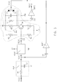
- the low-pass filter FLP whose input is reached by the signal V i .
- Said filter comprises a resistor R1 and a capacitor C1 connected as in the characteristic configuration of a low-pass filter of the first order.
- the output of the filter is connected to the control input of the voltage-controlled crystal oscillator VCXO and to the input of an amplifier BUF1 through a capacitor C2 of great capacity.
- the phase modulator PM consists of the transistor TR, the resonant circuit RIS and the resistors R2, R3, R4 which serve for the correct polarization of TR.
- the collector TR is also connected through a capacitor C4 of small capacity to the input of an amplifier BUF2 whose output is connected to the output terminal of the circuit which is the object of the present invention.
- the amplifier BUF2 receives the modulated signal present on the collector of TR and give it the necessary output power.
- the VCXO used has a frequency gain K vcxo of 1260 radiants/(voltxsecond), corresponding to approximately 200Hz/V. With this value of K vcxo the greatest possible swing of the control voltage V v causes a variation of the frequency of the VCXO on the order of ⁇ 1kHz which is more than sufficient to allow the PLL to phase lock the input signal, allowing also for any further variations in the frequency of the VCXO caused overall by ageing phenomena and thermal drifts.
Landscapes
- Stabilization Of Oscillater, Synchronisation, Frequency Synthesizers (AREA)
- Synchronisation In Digital Transmission Systems (AREA)
- Optical Communication System (AREA)
Applications Claiming Priority (2)
| Application Number | Priority Date | Filing Date | Title |
|---|---|---|---|
| ITMI912669 | 1991-10-08 | ||
| ITMI912669A IT1251706B (it) | 1991-10-08 | 1991-10-08 | Procedimento per ampliare la banda di risposta in frequenza di un oscillatore a cristallo controllato in tensione e relativo circuito. |
Publications (2)
| Publication Number | Publication Date |
|---|---|
| EP0536660A1 true EP0536660A1 (fr) | 1993-04-14 |
| EP0536660B1 EP0536660B1 (fr) | 1996-04-03 |
Family
ID=11360833
Family Applications (1)
| Application Number | Title | Priority Date | Filing Date |
|---|---|---|---|
| EP92116928A Expired - Lifetime EP0536660B1 (fr) | 1991-10-08 | 1992-10-02 | Procédé pour étendre la largeur de bande de la réponse d'un oscillateur à cristal commandé en tension et circuit associé |
Country Status (5)
| Country | Link |
|---|---|
| EP (1) | EP0536660B1 (fr) |
| DE (1) | DE69209605T2 (fr) |
| ES (1) | ES2084903T3 (fr) |
| GR (1) | GR3020102T3 (fr) |
| IT (1) | IT1251706B (fr) |
Cited By (3)
| Publication number | Priority date | Publication date | Assignee | Title |
|---|---|---|---|---|
| DE4424364A1 (de) * | 1993-07-14 | 1995-01-19 | Watkins Johnson Co | Referenzoszillator mit geringem Phasenrauschen |
| DE4436187A1 (de) * | 1993-10-13 | 1995-04-20 | Mitsubishi Electric Corp | Phasenstarrer Regelkreis, Oszillator und Signalprozessor |
| CN108631774A (zh) * | 2017-03-22 | 2018-10-09 | 中芯国际集成电路制造(上海)有限公司 | 锁相环及其启动电路、启动方法 |
Families Citing this family (1)
| Publication number | Priority date | Publication date | Assignee | Title |
|---|---|---|---|---|
| DE19953578A1 (de) | 1999-11-08 | 2001-05-23 | Mikron Ag Fuer Integrierte Mik | Vorrichtung und Verfahren zur Erzeugung eines Taktsignals |
Citations (3)
| Publication number | Priority date | Publication date | Assignee | Title |
|---|---|---|---|---|
| US2770730A (en) * | 1952-07-25 | 1956-11-13 | Int Standard Electric Corp | Frequency control circuit |
| US4009450A (en) * | 1975-04-14 | 1977-02-22 | Motorola, Inc. | Phase locked loop tracking filter having enhanced attenuation of unwanted signals |
| US4023115A (en) * | 1975-07-31 | 1977-05-10 | Societe Nationale D'etude Et De Construction De Moteurs D'aviation | Means for controlling the phase or frequency output of an oscillator in a loop circuit |
-
1991
- 1991-10-08 IT ITMI912669A patent/IT1251706B/it active IP Right Grant
-
1992
- 1992-10-02 DE DE69209605T patent/DE69209605T2/de not_active Expired - Fee Related
- 1992-10-02 EP EP92116928A patent/EP0536660B1/fr not_active Expired - Lifetime
- 1992-10-02 ES ES92116928T patent/ES2084903T3/es not_active Expired - Lifetime
-
1996
- 1996-05-30 GR GR960401468T patent/GR3020102T3/el unknown
Patent Citations (3)
| Publication number | Priority date | Publication date | Assignee | Title |
|---|---|---|---|---|
| US2770730A (en) * | 1952-07-25 | 1956-11-13 | Int Standard Electric Corp | Frequency control circuit |
| US4009450A (en) * | 1975-04-14 | 1977-02-22 | Motorola, Inc. | Phase locked loop tracking filter having enhanced attenuation of unwanted signals |
| US4023115A (en) * | 1975-07-31 | 1977-05-10 | Societe Nationale D'etude Et De Construction De Moteurs D'aviation | Means for controlling the phase or frequency output of an oscillator in a loop circuit |
Cited By (8)
| Publication number | Priority date | Publication date | Assignee | Title |
|---|---|---|---|---|
| DE4424364A1 (de) * | 1993-07-14 | 1995-01-19 | Watkins Johnson Co | Referenzoszillator mit geringem Phasenrauschen |
| GB2280554A (en) * | 1993-07-14 | 1995-02-01 | Watkins Johnson Co | Low phase noise locked oscillator |
| GB2280554B (en) * | 1993-07-14 | 1998-03-18 | Watkins Johnson Co | Low phase noise reference oscillator |
| DE4424364C2 (de) * | 1993-07-14 | 1998-10-15 | Watkins Johnson Co | Referenzoszillator mit geringem Phasenrauschen |
| DE4436187A1 (de) * | 1993-10-13 | 1995-04-20 | Mitsubishi Electric Corp | Phasenstarrer Regelkreis, Oszillator und Signalprozessor |
| DE4436187C2 (de) * | 1993-10-13 | 1998-09-17 | Mitsubishi Electric Corp | Phasenstarrer Regelkreis, Verwendung dieses Regelkreises sowie diesen Regelkreis enthaltender Signalprozessor |
| CN108631774A (zh) * | 2017-03-22 | 2018-10-09 | 中芯国际集成电路制造(上海)有限公司 | 锁相环及其启动电路、启动方法 |
| CN108631774B (zh) * | 2017-03-22 | 2021-07-13 | 中芯国际集成电路制造(上海)有限公司 | 锁相环及其启动电路、启动方法 |
Also Published As
| Publication number | Publication date |
|---|---|
| DE69209605D1 (de) | 1996-05-09 |
| DE69209605T2 (de) | 1996-09-26 |
| EP0536660B1 (fr) | 1996-04-03 |
| ES2084903T3 (es) | 1996-05-16 |
| ITMI912669A1 (it) | 1993-04-08 |
| ITMI912669A0 (it) | 1991-10-08 |
| IT1251706B (it) | 1995-05-19 |
| GR3020102T3 (en) | 1996-08-31 |
Similar Documents
| Publication | Publication Date | Title |
|---|---|---|
| EP1039640B1 (fr) | Circuit à boucle de verrouillage de phase | |
| US5635876A (en) | Phase difference and amplitude correction circuit | |
| EP0536660B1 (fr) | Procédé pour étendre la largeur de bande de la réponse d'un oscillateur à cristal commandé en tension et circuit associé | |
| US5708394A (en) | Bridge-stabilized oscillator circuit and method | |
| US5329250A (en) | Double phase locked loop circuit | |
| US6225872B1 (en) | Resonator having a selection circuit for selecting a resonance mode | |
| US6396356B1 (en) | Linearization scheme for voltage controlled oscillator | |
| JP2542928B2 (ja) | Fm変調器 | |
| EP0497801B1 (fr) | Boucle a verrouillage de phase servant a produire une porteuse de reference pour un detecteur coherent | |
| CA1142240A (fr) | Methode et dispositif pour contraindre un oscillateur a boucle a asservissement de phase a fonctionner a une frequence predeterminee lorsque les conditions de fonctionnement sont anormales | |
| US7271672B2 (en) | Voltage controlled LC tank oscillator | |
| US4796102A (en) | Automatic frequency control system | |
| US6546060B1 (en) | Direct modulating FSK transmitter for MCA | |
| US3873943A (en) | Low-distortion constant-amplitude oscillator | |
| US4914406A (en) | Voltage controlled oscillator free from free-run oscillating frequency adjustment | |
| US5483559A (en) | Phase-locked loop device, oscillator, and signal processor | |
| KR0138363B1 (ko) | 전압제어발진기 | |
| US5825258A (en) | Phase-locked loop circuit | |
| TWM681963U (zh) | 包含保持模組之鎖相迴路電路 | |
| KR920000459Y1 (ko) | 주파수 변조장치 | |
| JP3033049B2 (ja) | Dcfm回路の周波数ドリフト補正回路 | |
| EP0427717B1 (fr) | Circuit a boucle a verrouillage de phase | |
| JPH07106962A (ja) | 高速アナログpll回路および高速アナログpll回路におけるプリセット値の温度補償方法 | |
| Brunell | Theory of and a novel approach to high-stability frequency control circuits | |
| JP2859037B2 (ja) | 2重pll回路 |
Legal Events
| Date | Code | Title | Description |
|---|---|---|---|
| PUAI | Public reference made under article 153(3) epc to a published international application that has entered the european phase |
Free format text: ORIGINAL CODE: 0009012 |
|
| AK | Designated contracting states |
Kind code of ref document: A1 Designated state(s): DE ES FR GB GR IT SE |
|
| 17P | Request for examination filed |
Effective date: 19930804 |
|
| 17Q | First examination report despatched |
Effective date: 19950809 |
|
| GRAH | Despatch of communication of intention to grant a patent |
Free format text: ORIGINAL CODE: EPIDOS IGRA |
|
| GRAA | (expected) grant |
Free format text: ORIGINAL CODE: 0009210 |
|
| AK | Designated contracting states |
Kind code of ref document: B1 Designated state(s): DE ES FR GB GR IT SE |
|
| REF | Corresponds to: |
Ref document number: 69209605 Country of ref document: DE Date of ref document: 19960509 |
|
| ET | Fr: translation filed | ||
| REG | Reference to a national code |
Ref country code: ES Ref legal event code: FG2A Ref document number: 2084903 Country of ref document: ES Kind code of ref document: T3 |
|
| ITF | It: translation for a ep patent filed | ||
| REG | Reference to a national code |
Ref country code: GR Ref legal event code: FG4A Free format text: 3020102 |
|
| PLBE | No opposition filed within time limit |
Free format text: ORIGINAL CODE: 0009261 |
|
| 26N | No opposition filed | ||
| PGFP | Annual fee paid to national office [announced via postgrant information from national office to epo] |
Ref country code: GB Payment date: 19970909 Year of fee payment: 6 |
|
| PGFP | Annual fee paid to national office [announced via postgrant information from national office to epo] |
Ref country code: ES Payment date: 19971009 Year of fee payment: 6 |
|
| PGFP | Annual fee paid to national office [announced via postgrant information from national office to epo] |
Ref country code: SE Payment date: 19971029 Year of fee payment: 6 Ref country code: FR Payment date: 19971029 Year of fee payment: 6 |
|
| PGFP | Annual fee paid to national office [announced via postgrant information from national office to epo] |
Ref country code: GR Payment date: 19971031 Year of fee payment: 6 |
|
| PGFP | Annual fee paid to national office [announced via postgrant information from national office to epo] |
Ref country code: DE Payment date: 19971218 Year of fee payment: 6 |
|
| ITPR | It: changes in ownership of a european patent |
Owner name: CAMBIO NOME;ITALTEL S.P.A. |
|
| PG25 | Lapsed in a contracting state [announced via postgrant information from national office to epo] |
Ref country code: GB Free format text: LAPSE BECAUSE OF NON-PAYMENT OF DUE FEES Effective date: 19981002 |
|
| PG25 | Lapsed in a contracting state [announced via postgrant information from national office to epo] |
Ref country code: SE Free format text: LAPSE BECAUSE OF NON-PAYMENT OF DUE FEES Effective date: 19981003 Ref country code: ES Free format text: LAPSE BECAUSE OF NON-PAYMENT OF DUE FEES Effective date: 19981003 |
|
| PG25 | Lapsed in a contracting state [announced via postgrant information from national office to epo] |
Ref country code: GR Free format text: LAPSE BECAUSE OF NON-PAYMENT OF DUE FEES Effective date: 19981031 |
|
| GBPC | Gb: european patent ceased through non-payment of renewal fee |
Effective date: 19981002 |
|
| EUG | Se: european patent has lapsed |
Ref document number: 92116928.0 |
|
| PG25 | Lapsed in a contracting state [announced via postgrant information from national office to epo] |
Ref country code: FR Free format text: LAPSE BECAUSE OF NON-PAYMENT OF DUE FEES Effective date: 19990630 |
|
| REG | Reference to a national code |
Ref country code: FR Ref legal event code: ST |
|
| PG25 | Lapsed in a contracting state [announced via postgrant information from national office to epo] |
Ref country code: DE Free format text: LAPSE BECAUSE OF NON-PAYMENT OF DUE FEES Effective date: 19990803 |
|
| REG | Reference to a national code |
Ref country code: ES Ref legal event code: FD2A Effective date: 19991113 |
|
| PG25 | Lapsed in a contracting state [announced via postgrant information from national office to epo] |
Ref country code: IT Free format text: LAPSE BECAUSE OF NON-PAYMENT OF DUE FEES;WARNING: LAPSES OF ITALIAN PATENTS WITH EFFECTIVE DATE BEFORE 2007 MAY HAVE OCCURRED AT ANY TIME BEFORE 2007. THE CORRECT EFFECTIVE DATE MAY BE DIFFERENT FROM THE ONE RECORDED. Effective date: 20051002 |