EP0536689B1 - Schaltung mit veränderlicher Verzögerung - Google Patents
Schaltung mit veränderlicher Verzögerung Download PDFInfo
- Publication number
- EP0536689B1 EP0536689B1 EP92117027A EP92117027A EP0536689B1 EP 0536689 B1 EP0536689 B1 EP 0536689B1 EP 92117027 A EP92117027 A EP 92117027A EP 92117027 A EP92117027 A EP 92117027A EP 0536689 B1 EP0536689 B1 EP 0536689B1
- Authority
- EP
- European Patent Office
- Prior art keywords
- circuit
- transistor
- transistors
- power source
- series
- Prior art date
- Legal status (The legal status is an assumption and is not a legal conclusion. Google has not performed a legal analysis and makes no representation as to the accuracy of the status listed.)
- Expired - Lifetime
Links
Images







Classifications
-
- H—ELECTRICITY
- H03—ELECTRONIC CIRCUITRY
- H03K—PULSE TECHNIQUE
- H03K5/00—Manipulating of pulses not covered by one of the other main groups of this subclass
- H03K5/13—Arrangements having a single output and transforming input signals into pulses delivered at desired time intervals
- H03K5/133—Arrangements having a single output and transforming input signals into pulses delivered at desired time intervals using a chain of active delay devices
-
- H—ELECTRICITY
- H03—ELECTRONIC CIRCUITRY
- H03K—PULSE TECHNIQUE
- H03K5/00—Manipulating of pulses not covered by one of the other main groups of this subclass
- H03K5/13—Arrangements having a single output and transforming input signals into pulses delivered at desired time intervals
- H03K5/131—Digitally controlled
-
- H—ELECTRICITY
- H03—ELECTRONIC CIRCUITRY
- H03K—PULSE TECHNIQUE
- H03K5/00—Manipulating of pulses not covered by one of the other main groups of this subclass
- H03K2005/00013—Delay, i.e. output pulse is delayed after input pulse and pulse length of output pulse is dependent on pulse length of input pulse
- H03K2005/00019—Variable delay
- H03K2005/00058—Variable delay controlled by a digital setting
- H03K2005/00065—Variable delay controlled by a digital setting by current control, e.g. by parallel current control transistors
-
- H—ELECTRICITY
- H03—ELECTRONIC CIRCUITRY
- H03K—PULSE TECHNIQUE
- H03K5/00—Manipulating of pulses not covered by one of the other main groups of this subclass
- H03K2005/00013—Delay, i.e. output pulse is delayed after input pulse and pulse length of output pulse is dependent on pulse length of input pulse
- H03K2005/0015—Layout of the delay element
- H03K2005/00195—Layout of the delay element using FET's
Definitions
- the present invention relates to a variable delay circuit according to the preamble of the claim 1.
- variable delay circuit is known from WO/A 88/08642.
- This known variable delay circuit is formed as an inverting variable delay circuit and comprises:
- CMOS driver circuit for integrated circuits which is capable of operating in two modes.
- this two-mode driver circuit comprises a plurality of MOS transistors which are coupled in parallel. The number of MOS transistors which are ON and coupled in parallel is changed, so as to change the driving capacity of the circuit.
- the delay time of the inverter circuit is varied basically as a result of the resistance that is varied by changing the number of MOS transistors which are turned ON/OFF.
- variable delay circuits are known with which the delay time is varied by varying the power supply voltage and consequently varying the operation speed of the entire circuit.
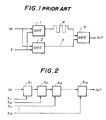
- FIG.1 shows an example of a conventional variable delay circuit.
- This variable delay circuit includes gates 1, 2 and 3 which are coupled via wirings 4 and 5.
- the length of the wiring 4 is longer than that of the wiring 5 so that the stray capacitance of the wiring 4 is greater than that of the wiring 5.
- IN, S and OUT respectively denote an input signal, a selection signal and an output signal.
- the gate 1 becomes conductive during a low-level period of the selection signal S and becomes non-conductive during a high-level period of the selection signal S.
- the gate 2 becomes conductive during the high-level period of the selection signal S and becomes non-conductive during the low-level period of the selection signal S.
- the gate 3 is conductive regardless of the level of the selection signal S.
- the input signal IN passes through the gate 1, the wiring 4 and the gate 3 and is output as the output signal OUT.
- the input signal IN passes through the gate 2, the wiring 5 and the gate 3 and is output as the output signal OUT.
- the lengths of the wirings 4 and 5 are determined so that a delay time of 550 ps, for example, is obtained when the selection signal S has the low level, and a delay time of 500 ps, for example, is obtained when the selection signal S has the high level.
- FIG.2 shows a case where a circuit for finely adjusting the delay time is formed by connecting 10 variable delay circuits 6 1 through 6 10 respectively having the same construction as the variable delay circuit shown in FIG.1.
- S 1 through S 10 respectively denote selection signals which are input to the variable delay circuits 6 1 through 6 10 and correspond to the selection signal S.
- variable delay circuit shown in FIG.1 obtains the different delay time depending on the different lengths of the wirings 4 and 5. For this reason, there is a problem in that it is difficult to easily obtain a fine time difference, and the circuit for finely adjusting the delay time cannot be formed with ease.
- variable delay circuit of the present invention it is possible to easily obtain a plurality of delay times having fine time differences with respect to a high-level output signal.
- FIG.3 shows the first aspect of the present invention.
- a pull-up circuit 142 which carries out a pull-up operation based on an input signal IN which is input to an input terminal 145 is coupled between a power source line 140 which supplies a power source voltage V DD and an output terminal 141.
- a pull-down circuit 144 which carries out a pull-down operation based on the input signal IN and is coupled between the output terminal 141 and a power source line 143 which supplies a power source voltage V SS which is lower than the power source voltage V DD .
- This pull- down circuit 144 has a variable delay time which is set responsive to a selection signal S which is received via a terminal 148.
- the pull-down circuit 144 By the provision of the pull-down circuit 144, it is possible to select the delay time of the falling edge of an output signal OUT which is output via the output terminal 141 as shown in FIG.3 (b). It is possible to easily obtain a plurality of delay times having fine time differences.
- FIG.4 shows the second aspect of the present invention.
- a pull-up circuit 146 which carries out a pull-up operation based on the input signal IN which is input to the input terminal 145 is coupled between the power source line 140 which supplies the power source voltage V DD and the output terminal 141.
- a pull-down circuit 147 which carries out a pull-down operation based on the input signal IN and is coupled between the output terminal 141 and the power source line 143 which supplies the power source voltage V SS which is lower than the power source voltage V DD .
- the pull-up circuit 146 has a variable delay time which is set responsive to the selection signal S which is received via the terminal 148.
- the pull-up circuit 146 By the provision of the pull-up circuit 146, it is possible to select the delay time of the rising edge of the output signal OUT which is output via the output terminal 141 as shown in FIG.4 (b). It is possible to easily obtain a plurality of delay times having fine time differences.
- FIG.5 shows the first embodiment.
- An input signal IN is input to an input terminal 9, a selection signal S is input to an input terminal 10, and an output signal OUT is output from an output terminal 11.
- a power source line 12 supplies a power source voltage V DD
- a power source line 13 supplies a power source voltage V SS , where V SS ⁇ V DD .
- the variable delay circuit includes a p-channel metal insulator semiconductor (MIS) or metal oxide semiconductor (MOS) transistor 14, n-channel MIS or MOS transistors 15 through 18, and an inverter 19 which are connected as shown.
- the transistor 14 forms a pull-up circuit, and the transistors 15 through 18 form a pull-down circuit.
- MIS metal insulator semiconductor
- MOS metal oxide semiconductor
- a gate of the transistor 15 which is connected to the first stage counted from the output terminal 11 is connected to the input terminal 9.
- a gate of the transistor 18 which is connected to the second stage counted from the output terminal 11 is connected to the input terminal 9.
- a gate of the transistor 16 is connected to the input terminal 9 for receiving the selection signal S.
- a gate of the transistor 17 is connected to an output terminal of the inverter 19.
- one of the series circuit made up of the transistors 15 and 16 and the series circuit made up of the transistors 17 and 18 is selected and made active as a pull-down circuit in response to the selection signal S.
- This selection of the series circuits forms a characterizing feature of this embodiment, and is used as one means of obtaining two kinds of delay times as will be described later.
- FIGS.6 and 7 are circuit diagrams for explaining the operation of this embodiment, and FIG.8 is a time chart for explaining the operation of this embodiment.
- the transistor 16 becomes non-conductive (that is, OFF) and the transistor 17 becomes conductive (that is, ON) during a low-level period of the selection signal S.
- FIG.6 shows an equivalent circuit of this embodiment during the low-level period of the selection signal S, and in FIG.6, the transistor 17 is shown as an ON-resistance.
- the transistor 14 is ON, the transistor 18 is OFF, and the output signal OUT has a high level.
- the transistor 14 turns OFF, the transistor 18 turns ON, and the output signal OUT is inverted from the high level to a low level.
- the transistor 18 turns ON at the time when the input signal IN rises to a threshold voltage V th18 of the transistor 18.
- a dotted line 20 shows the transition of the output signal OUT in this case.
- the transistor 16 is ON and the transistor 17 is OFF during a high-level period of the selection signal S.
- FIG.7 shows an equivalent circuit of this embodiment during the high-level period of the selection signal S, and in FIG.7, the transistor 16 is shown as an ON-resistance.
- the transistor 14 is ON, the transistor 15 is OFF and the output signal OUT has the high level.
- the transistor 14 turns OFF, the transistor 15 turns ON, and the output signal OUT is inverted from the high level to the low level.
- the transistor 15 turns ON at the time when the input signal IN rises to a voltage which is the sum of a voltage drop V 16 introduced by an ON-resistance of the transistor 16 and a threshold voltage V th15 of the transistor 15.
- a solid line 21 shows the transition of the output signal OUT in this case.
- this first embodiment it is possible to easily obtain two kinds of delay times having a fine time difference with respect to the low-level output signal OUT by the selection made in response to the selection signal S. Hence, this embodiment may be easily applied to a circuit for finely adjusting the delay time and the like.
- FIG.9 shows the second embodiment.
- An input signal IN is input to an input terminal 22, a selection signal S is input to an input terminal 23, and an output signal OUT is output from an output terminal 24.
- a power source line 25 supplies a power source voltage V DD
- a power source line 26 supplies a power source voltage V SS , where V SS ⁇ V DD .
- the variable delay circuit includes a p-channel MIS or MOS transistor 27, n-channel MIS or MOS transistors 28 through 33, and an inverter 34 which are connected as shown.
- the transistor 27 forms a pull-up circuit
- the transistors 28 through 33 form a pull-down circuit.
- a gate of the transistor 28 which is connected to the first stage counted from the output terminal 24 is connected to the input terminal 22.
- a gate of the transistor 32 which is connected to the third stage counted from the output terminal 24 is connected to the input terminal 22.
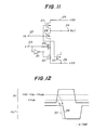
- FIGS.10 and 11 are circuit diagrams for explaining the operation of this embodiment
- FIG.12 is a time chart for explaining the operation of this embodiment.
- the transistors 29 and 30 become OFF and the transistors 31 and 32 become ON during a low-level period of the selection signal S.
- FIG.10 shows an equivalent circuit of this embodiment during the low-level period of the selection signal S, and in FIG.10, the transistors 31 and 32 are shown as ON-resistances.
- the transistor 27 is ON, the transistor 33 is OFF, and the output signal OUT has a high level.
- the transistor 27 turns OFF, the transistor 33 turns ON, and the output signal OUT is inverted from the high level to a low level.
- the transistor 33 turns ON at the time when the input signal IN rises to a threshold voltage V th33 of the transistor 33.
- a dotted line 35 shows the transition of the output signal OUT in this case.
- the transistors 29 and 30 are ON and the transistors 31 and 32 are OFF during a high-level period of the selection signal S.
- FIG.11 shows an equivalent circuit of this embodiment during the high-level period of the selection signal S, and in FIG.11, the transistors 29 and 30 are shown as ON-resistances.
- the transistor 27 is ON, the transistor 28 is OFF and the output signal OUT has the high level.
- the transistor 27 turns OFF, the transistor 28 turns ON, and the output signal OUT is inverted from the high level to the low level.
- the transistor 28 turns ON at the time when the input signal IN rises to a voltage which is the sum of a voltage drop V 30 introduced by an ON-resistance of the transistor 30, a voltage drop V 29 introduced by an ON-resistance of the transistor 19 and a threshold voltage V th28 of the transistor 28.
- a solid line 36 shows the transition of the output signal OUT in this case.
- this second embodiment it is possible to easily obtain two kinds of delay times larger than those of the first embodiment and having a fine time difference with respect to the low-level output signal OUT by the selection made in response to the selection signal S.
- this embodiment may be easily applied to a circuit for finely adjusting the delay time and the like.
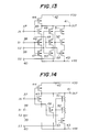
- FIG.13 shows the third embodiment.
- An input signal IN is input to an input terminal 37
- selection signals S1, S2 and S3 are respectively input to input terminals 38, 39 and 40
- an output signal OUT is output from an output terminal 41.
- a power source line 42 supplies a power source voltage V DD
- a power source line 43 supplies a power source voltage V SS , where V SS ⁇ V DD .
- the variable delay circuit includes a p-channel MIS or MOS transistor 44, and n-channel MIS or MOS transistors 45 through 53 which are connected as shown.
- the transistor 44 forms a pull-up circuit
- the transistors 45 through 53 form a pull-down circuit.
- a gate of the transistor 45 which is connected to the first stage counted from the output terminal 41 is connected to the input terminal 37.
- a gate of the transistor 49 which is connected to the second stage counted from the output terminal 41 is connected to the input terminal 37.
- a gate of the transistor 53 which is connected to the third stage counted from the output terminal 41 is connected to the input terminal 37.
- the gate of only one of the transistors connected to the same stage counted from the output terminal 41 or the power source line 43 is connected to the input terminal 37.
- one of the series circuit made up of the transistors 45, 46 and 47, the series circuit made up of the transistors 48, 49 and 50, and the series circuit made up of the transistors 51, 52 and 53 is selected and made active as a pull-down circuit in response to the selection signals S1, S2 and S3.
- This selection of the series circuits forms a characterizing feature of this embodiment, and is used as one means of obtaining three kinds of delay times as will be described later.
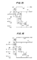
- FIGS.14, 15 and 16 are circuit diagrams for explaining the operation of this embodiment
- FIG.17 is a time chart for explaining the operation of this embodiment.
- the transistors 46, 47, 48 and 50 become OFF and the transistors 51 and 52 become ON if the selection signals S1 and S2 both have a low level and the selection signal S3 has a high level.
- FIG.14 shows an equivalent circuit of this embodiment for the case where the selection signals S1 and S2 both have the low level and the selection signal S3 has the high level, and in FIG.14, the transistors 51 and 52 are shown as ON-resistances.
- the transistor 44 is ON, the transistor 53 is OFF, and the output signal OUT has a high level.
- the transistor 44 turns OFF, the transistor 53 turns ON, and the output signal OUT is inverted from the high level to a low level.
- the transistor 53 turns ON at the time when the input signal IN rises to a threshold voltage V th53 of the transistor 53.
- a dotted line 54 shows the transition of the output signal OUT in this case.
- the transistors 46, 47, 51 and 52 are OFF and the transistors 48 and 50 are ON when the selection signals S1 and S3 have the low level and the selection signal S2 has the high level.
- FIG.15 shows an equivalent circuit of this embodiment for the case where the selection signals S1 and S3 have the low level and the selection signal S2 has the high level, and in FIG.15, the transistors 48 and 50 are shown as ON-resistances.
- the transistor 44 is ON, the transistor 49 is OFF and the output signal OUT has the high level.
- the transistor 44 turns OFF, the transistor 49 turns ON, and the output signal OUT is inverted from the high level to the low level.
- the transistor 49 turns ON at the time when the input signal IN rises to a voltage which is the sum of a voltage drop V 50 introduced by an ON-resistance of the transistor 50 and a threshold voltage V th49 of the transistor 49.
- a solid line 55 shows the transition of the output signal OUT in this case.
- FIG.16 shows an equivalent circuit of this embodiment for the case where the selection signal S1 has the high level and the selection signals S2 and S3 have the low level, and in FIG.16, the transistors 46 and 47 are shown as ON-resistances.
- the transistor 44 is ON, the transistor 45 is OFF and the output signal OUT has the high level.
- the transistor 44 turns OFF, the transistor 45 turns ON, and the output signal OUT is inverted from the high level to the low level.
- the transistor 45 turns ON at the time when the input signal IN rises to a voltage which is the sum of a voltage drop V 47 introduced by an ON-resistance of the transistor 47, a voltage drop V 46 introduced by an ON-resistance of the transistor 46 and a threshold voltage V th45 of the transistor 45.
- a two dot chain line 56 shows the transition of the output signal OUT in this case.
- this third embodiment it is possible to easily obtain three kinds of delay times having a fine time difference with respect to the low-level output signal OUT by the selection made in response to the selection signals S1, S2 and S3. Hence, this embodiment may be easily applied to a circuit for finely adjusting the delay time and the like.
- FIG.18 shows the fourth embodiment.
- An input signal IN is input to an input terminal 57
- a selection signal S is input to an input terminal 58
- an output signal OUT is output from an output terminal 59.
- a power source line 60 supplies a power source voltage V DD
- a power source line 61 supplies a power source voltage V SS , where V SS ⁇ V DD .
- the variable delay circuit includes a p-channel MIS or MOS transistor 62, an NPN transistor 63, a resistor 64 for drawing the base charge of the NPN transistor 63, n-channel MIS or MOS transistors 65 through 68, an inverter 69, an NPN transistor 70, and a resistor 71 for drawing the base charge of the NPN transistor 70 which are connected as shown.
- the transistors 62 and 63 and the resistor 64 form a pull-up circuit.
- the transistors 65 through 68, the inverter 69, the transistor 70 and the resistor 71 form a pull-down circuit.
- a gate of the transistor 65 which is connected to the first stage counted from the output terminal 59 is connected to the input terminal 57.
- a gate of the transistor 68 which is connected to the second stage counted from the output terminal 59 is connected to the input terminal 57.
- a gate of the transistor 66 is connected to the input terminal 58 for receiving the selection signal S.
- a gate of the transistor 67 is connected to an output terminal of the inverter 69.
- one of the series circuit made up of the transistors 65 and 66 and the series circuit made up of the transistors 67 and 68 is selected and made active in response to the selection signal S, so as to select the pull-down circuit formed by the transistors 65, 66 and 70 and the resistor 71 or the pull-down circuit formed by the transistors 67, 68 and 70 and the resistor 71.
- This selection of the series circuits or, the pull-down circuits forms a characterizing feature of this embodiment, and is used as one means of obtaining two kinds of delay times as will be described later.
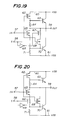
- FIGS.19 and 20 are circuit diagrams for explaining the operation of this embodiment
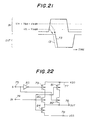
- FIG.21 is a time chart for explaining the operation of this embodiment.
- the transistor 66 becomes OFF and the transistor 67 becomes ON during a low-level period of the selection signal S.
- FIG.19 shows an equivalent circuit of this embodiment during the low-level period of the selection signal S, and in FIG.19, the transistor 67 is shown as an ON-resistance.
- the transistor 62 is ON, the NPN transistor 63 is ON, the transistor 68 is OFF, the NPN transistor 70 is OFF, and the output signal OUT has a high level.
- the transistor 62 turns OFF, the NPN transistor 63 turns OFF, the transistor 68 turns ON, the NPN transistor 70 turns ON, and the output signal OUT is inverted from the high level to a low level.
- the transistor 68 turns ON at the time when the input signal IN rises to a voltage which is the sum of a voltage drop V 71 introduced by the resistor 71 and a threshold voltage V th68 of the transistor 68.
- a dotted line 72 shows the transition of the output signal OUT in this case.
- the transistor 66 is ON and the transistor 67 is OFF during a high-level period of the selection signal S.
- FIG.20 shows an equivalent circuit of this embodiment during the high-level period of the selection signal S, and in FIG.20, the transistor 66 is shown as an ON-resistance.
- the transistor 62 is ON, the NPN transistor 63 is ON, the transistor 65 is OFF, the NPN transistor 70 is OFF and the output signal OUT has the high level.
- the transistor 62 turns OFF, the NPN transistor 63 turns OFF, the transistor 65 turns ON, the NPN transistor 70 turns ON and the output signal OUT is inverted from the high level to the low level.
- the transistor 65 turns ON at the time when the input signal IN rises to a voltage which is the sum of a voltage drop V 71 introduced by the resistor 71, a voltage drop V 66 introduced by an ON-resistance of the transistor 66 and a threshold voltage V th65 of the transistor 65.
- a solid line 73 shows the transition of the output signal OUT in this case.
- this fourth embodiment it is possible to easily obtain two kinds of delay times having a fine time difference with respect to the low-level output signal OUT by the selection made in response to the selection signal S using a BiCMOS structure. Hence, this embodiment may be easily applied to a circuit for finely adjusting the delay time and the like.
- FIG.22 shows the fifth embodiment.
- An input signal IN is input to an input terminal 74
- a selection signal S is input to an input terminal 75
- an output signal OUT is output from an output terminal 76.
- a power source line 77 supplies a power source voltage V DD
- a power source line 78 supplies a power source voltage V SS , where V SS ⁇ V DD .
- the variable delay circuit includes a p-channel MIS or MOS transistors 79 through 82, an inverter 83, and an n-channel MIS or MOS transistor 84 which are connected as shown.
- the transistors 79 through 82 form a pull-up circuit
- the transistor 84 forms a pull-down circuit.
- a gate of the transistor 80 which is connected to the second stage counted from the power source line 77 is connected to the input terminal 74.
- a gate of the transistor 81 which is connected to the first stage counted from the power source line 77 is connected to the input terminal 74.
- a gate of the transistor 79 is connected to an output terminal of the inverter 83.
- a gate of the transistor 82 is connected to the input terminal 75 for receiving the selection signal S.
- one of the series circuit made up of the transistors 79 and 80 and the series circuit made up of the transistors 81 and 82 is selected and made active as a pull-up circuit in response to the selection signal S.
- This selection of the series circuits forms a characterizing feature of this embodiment, and is used as one means of obtaining two kinds of delay times as will be described later.
- FIGS.23 and 24 are circuit diagrams for explaining the operation of this embodiment
- FIG.25 is a time chart for explaining the operation of this embodiment.
- the transistor 79 becomes OFF and the transistor 82 becomes ON during a low-level period of the selection signal S.
- FIG.23 shows an equivalent circuit of this embodiment during the low-level period of the selection signal S, and in FIG.23, the transistor 82 is shown as an ON-resistance.
- the transistor 81 is OFF, the transistor 84 is ON, and the output signal OUT has a low level.
- the transistor 81 turns ON, the transistor 84 turns OFF, and the output signal OUT is inverted from the low level to a high level.
- the transistor 81 turns ON at the time when the input signal IN falls to a voltage V DD -V th81 , where V th81 denotes a threshold voltage of the transistor 81.
- V th81 denotes a threshold voltage of the transistor 81.
- a dotted line 85 shows the transition of the output signal OUT in this case.
- the transistor 79 is ON and the transistor 82 is OFF during a high-level period of the selection signal S.
- FIG.24 shows an equivalent circuit of this embodiment during the high-level period of the selection signal S, and in FIG.24, the transistor 79 is shown as an ON-resistance.
- the transistor 80 is OFF, the transistor 84 is ON and the output signal OUT has the low level.
- the transistor 80 turns ON, the transistor 84 turns OFF, and the output signal OUT is inverted from the low level to the high level.
- the transistor 80 turns ON at the time when the input signal IN falls to a voltage V DD -V 79 -V th80 , where V 79 denotes a voltage drop introduced by an ON-resistance of the transistor 79 and V th80 denotes a threshold voltage of the transistor 80.
- V 79 denotes a voltage drop introduced by an ON-resistance of the transistor 79
- V th80 denotes a threshold voltage of the transistor 80.
- a solid line 86 shows the transition of the output signal OUT in this case.
- this fifth embodiment it is possible to easily obtain two kinds of delay times having a fine time difference with respect to the high-level output signal OUT by the selection made in response to the selection signal S. Hence, this embodiment may be easily applied to a circuit for finely adjusting the delay time and the like.
- FIG.26 shows the sixth embodiment.
- An input signal IN is input to an input terminal 87
- a selection signal S is input to an input terminal 88
- an output signal OUT is output from an output terminal 89.
- a power source line 90 supplies a power source voltage V DD
- a power source line 91 supplies a power source voltage V SS , where V SS ⁇ V DD .
- the variable delay circuit includes p-channel MIS or MOS transistors 92 through 97, an inverter 98, and an n-channel MIS or MOS transistor 99 which are connected as shown.
- the transistors 92 through 97 form a pull-up circuit
- the transistor 99 forms a pull-down circuit.
- a gate of the transistor 94 which is connected to the third stage counted from the power source line 90 is connected to the input terminal 87.
- a gate of the transistor 95 which is connected to the first stage counted from the power source line 90 is connected to the input terminal 87.
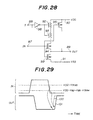
- FIGS.27 and 28 are circuit diagrams for explaining the operation of this embodiment
- FIG.29 is a time chart for explaining the operation of this embodiment.
- the transistors 92 and 93 become OFF and the transistors 96 and 97 become ON during a low-level period of the selection signal S.
- FIG.27 shows an equivalent circuit of this embodiment during the low-level period of the selection signal S, and in FIG.27, the transistors 96 and 97 are shown as ON-resistances.
- the transistor 95 is OFF, the transistor 99 is ON, and the output signal OUT has a low level.
- the transistor 95 turns ON, the transistor 99 turns OFF, and the output signal OUT is inverted from the low level to a high level.
- the transistor 95 turns ON at the time when the input signal IN falls to a voltage V DD -V th95 , where V th95 denotes a threshold voltage of the transistor 95.
- V th95 denotes a threshold voltage of the transistor 95.
- a dotted line 100 shows the transition of the output signal OUT in this case.
- the transistors 92 and 93 are ON and the transistors 96 and 97 are OFF during a high-level period of the selection signal S.
- FIG.28 shows an equivalent circuit of this embodiment during the high-level period of the selection signal S, and in FIG.28, the transistors 92 and 93 are shown as ON-resistances.
- the transistor 94 is OFF, the transistor 99 is ON and the output signal OUT has the low level.
- the transistor 94 turns ON, the transistor 99 turns OFF, and the output signal OUT is inverted from the low level to the high level.
- the transistor 94 turns ON at the time when the input signal IN falls to a voltage V DD -V 92 -V 93 -V th94 , where V 92 denotes a voltage drop introduced by the ON resistance of the transistor 92, V 93 denotes a voltage drop introduced by the ON-resistance of the transistor 93, and V th94 denotes a threshold voltage of the transistor 94.
- V 92 denotes a voltage drop introduced by the ON resistance of the transistor 92
- V 93 denotes a voltage drop introduced by the ON-resistance of the transistor 93
- V th94 denotes a threshold voltage of the transistor 94.
- a solid line 101 shows the transition of the output signal OUT in this case.
- this sixth embodiment it is possible to easily obtain two kinds of delay times larger than those of the fifth embodiment and having a fine time difference with respect to the high-level output signal OUT by the selection made in response to the selection signal S.
- this embodiment may be easily applied to a circuit for finely adjusting the delay time and the like.
- FIG.30 shows the seventh embodiment.
- An input signal IN is input to an input terminal 102
- selection signals S1, S2 and S3 are respectively input to input terminals 103, 104 and 105
- an output signal OUT is output from an output terminal 106.
- a power source line 107 supplies a power source voltage V DD
- a power source line 108 supplies a power source voltage V SS , where V SS ⁇ V DD .
- the variable delay circuit includes p-channel MIS or MOS transistors 109 through 117, and an n-channel MIS or MOS transistor 118 which are connected as shown.
- the transistors 109 through 117 form a pull-up circuit
- the transistor 118 forms a pull-down circuit.
- a gate of the transistor 111 which is connected to the third stage counted from the power source line 107 is connected to the input terminal 102.
- a gate of the transistor 113 which is connected to the second stage counted from the power source line 107 is connected to the input terminal 102.
- a gate of the transistor 115 which is connected to the first stage counted from the power source line 107 is connected to the input terminal 102.
- the gate of only one of the transistors connected to the same stage counted from the power source line 107 or the output terminal 106 is connected to the input terminal 102.
- one of the series circuit made up of the transistors 109, 110 and 111, the series circuit made up of the transistors 112, 113 and 114, and the series circuit made up of the transistors 115, 116 and 117 is selected and made active as a pull-up circuit in response to the selection signals S1, S2 and S3.
- This selection of the series circuits forms a characterizing feature of this embodiment, and is used as one means of obtaining three kinds of delay times as will be described later.
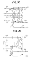
- FIGS.31, 32 and 33 are circuit diagrams for explaining the operation of this embodiment
- FIG.34 is a time chart for explaining the operation of this embodiment.
- the transistors 109, 110, 112 and 114 become OFF and the transistors 116 and 117 become ON if the selection signals S1 and S2 both have a high level and the selection signal S3 has a low level.
- FIG.31 shows an equivalent circuit of this embodiment for the case where the selection signals S1 and S2 both have the high level and the selection signal S3 has the low level, and in FIG.31, the transistors 116 and 117 are shown as ON-resistances.
- the transistor 115 is OFF, the transistor 118 is ON, and the output signal OUT has a low level.
- the transistor 115 turns ON, the transistor 118 turns OFF, and the output signal OUT is inverted from the low level to a high level.
- the transistor 115 turns ON at the time when the input signal IN falls to a voltage V DD -V th115 , where V th115 denotes a threshold voltage of the transistor 115.
- V th115 denotes a threshold voltage of the transistor 115.
- a dotted line 119 shows the transition of the output signal OUT in this case.
- the transistors 109, 110, 116 and 117 are OFF and the transistors 112 and 114 are ON when the selection signals S1 and S3 have the high level and the selection signal S2 has the low level.
- FIG.32 shows an equivalent circuit of this embodiment for the case where the selection signals S1 and S3 have the high level and the selection signal S2 has the low level, and in FIG.32, the transistors 112 and 114 are shown as ON-resistances.
- the transistor 113 is OFF, the transistor 118 is ON and the output signal OUT has the low level.
- the transistor 113 turns ON, the transistor 118 turns OFF, and the output signal OUT is inverted from the low level to the high level.
- the transistor 113 turns ON at the time when the input signal IN falls to a voltage V DD -V 112 -V th113 , where V 112 denotes a voltage drop introduced by the ON-resistance of the transistor 112 and V th113 denotes a threshold voltage of the transistor 113.
- a solid line 120 shows the transition of the output signal OUT in this case.
- FIG.33 shows an equivalent circuit of this embodiment for the case where the selection signal S1 has the low level and the selection signals S2 and S3 have the high level, and in FIG.33, the transistors 109 and 110 are shown as ON-resistances.
- the transistor 111 is OFF, the transistor 118 is ON and the output signal OUT has the low level.
- the transistor 111 turns ON, the transistor 118 turns OFF, and the output signal OUT is inverted from the low level to the high level.
- the transistor 111 turns ON at the time when the input signal IN falls to a voltage V DD -V 109 -V 110 -V th111 , where V 109 denotes a voltage drop introduced by the ON-resistance of the transistor 109, V 110 denotes the voltage introduced by the ON-resistance of the transistor 110, and V th111 denotes a threshold voltage of the transistor 111.
- V 109 denotes a voltage drop introduced by the ON-resistance of the transistor 109
- V 110 denotes the voltage introduced by the ON-resistance of the transistor 110
- V th111 denotes a threshold voltage of the transistor 111.
- a two dot chain line 121 shows the transition of the output signal OUT in this case.
- this seventh embodiment it is possible to easily obtain three kinds of delay times having a fine time difference with respect to the high-level output signal OUT by the selection made in response to the selection signals S1, S2 and S3. Hence, this embodiment may be easily applied to a circuit for finely adjusting the delay time and the like.
- FIG.35 shows the eighth embodiment.
- An input signal IN is input to an input terminal 122
- a selection signal S is input to an input terminal 123
- an output signal OUT is output from an output terminal 124.
- a power source line 125 supplies a power source voltage V DD
- a power source line 126 supplies a power source voltage V SS , where V SS ⁇ V DD .
- the variable delay circuit includes p-channel MIS or MOS transistors 127 through 130, an inverter 131, an NPN transistor 132, a resistor 133 for drawing the base charge of the NPN transistor 132, an n-channel MIS or MOS transistor 134, an NPN transistor 135, and a resistor 136 for drawing the base charge of the NPN transistor 135 which are connected as shown.
- the transistors 127 through 130, the inverter 131, the NPN transistor 132 and the resistor 133 form a pull-up circuit.
- the transistors 134 and 135 and the resistor 136 form a pull-down circuit.
- a gate of the transistor 128 which is connected to the second stage counted from the power source line 125 is connected to the input terminal 122.
- a gate of the transistor 129 which is connected to the first stage counted from the power source line 125 is connected to the input terminal 122.
- a gate of the transistor 127 is connected to an output terminal of the inverter 131.
- a gate of the transistor 130 is connected to the input terminal 123 for receiving the selection signal S.
- one of the series circuit made up of the transistors 127 and 128 and the series circuit made up of the transistors 129 and 130 is selected and made active in response to the selection signal S, so as to select the pull-up circuit formed by the transistors 127, 128 and 132 and the resistor 133 or the pull-up circuit formed by the transistors 129, 130 and 132 and the resistor 133.
- This selection of the series circuits or, the pull-up circuits forms a characterizing feature of this embodiment, and is used as one means of obtaining two kinds of delay times as will be described later.
- FIGS.36 and 37 are circuit diagrams for explaining the operation of this embodiment, and FIG.38 is a time chart for explaining the operation of this embodiment.
- the transistor 127 becomes OFF and the transistor 130 becomes ON during a low-level period of the selection signal S.
- FIG.36 shows an equivalent circuit of this embodiment during the low-level period of the selection signal S, and in FIG.36, the transistor 130 is shown as an ON-resistance.
- the transistor 129 is OFF, the NPN transistor 132 is OFF, the transistor 134 is ON, the NPN transistor 135 is ON, and the output signal OUT has a low level.
- the transistor 129 turns ON, the NPN transistor 132 turns ON, the transistor 134 turns OFF, the NPN transistor 135 turns OFF, and the output signal OUT is inverted from the low level to a high level.
- the transistor 129 turns ON at the time when the input signal IN falls to a voltage V DD -V th129 , where V th129 denotes a threshold voltage of the transistor 129.
- V th129 denotes a threshold voltage of the transistor 129.
- a dotted line 137 shows the transition of the output signal OUT in this case.
- the transistor 127 is ON and the transistor 130 is OFF during a high-level period of the selection signal S.
- FIG.37 shows an equivalent circuit of this embodiment during the high-level period of the selection signal S, and in FIG.37, the transistor 127 is shown as an ON-resistance.
- the transistor 128 is OFF, the NPN transistor 132 is OFF, the transistor 134 is ON, the NPN transistor 135 is ON and the output signal OUT has the low level.
- the transistor 128 turns ON, the NPN transistor 132 turns ON, the transistor 134 turns OFF, the NPN transistor 135 turns OFF and the output signal OUT is inverted from the low level to the high level.
- the transistor 128 turns ON at the time when the input signal IN falls to a voltage V DD -V 127 -V th128 , where V 127 denotes a voltage drop introduced by the ON-resistance of the transistor 127 and V th128 denotes a threshold voltage of the transistor 128.
- V 127 denotes a voltage drop introduced by the ON-resistance of the transistor 127
- V th128 denotes a threshold voltage of the transistor 128.
- a solid line 138 shows the transition of the output signal OUT in this case.
- this eighth embodiment it is possible to easily obtain two kinds of delay times having a fine time difference with respect to the low-level output signal OUT by the selection made in response to the selection signal S using a BiCMOS structure. Hence, this embodiment may be easily applied to a circuit for finely adjusting the delay time and the like.
- variable delay circuits having the construction described in any of the embodiments may be connected as shown in FIG.2, for example, so as to obtain an arbitrary number of delay times having fine time differences.
- present invention is also suited for obtaining the delay times having the fine time differences in a gate array circuit.
Landscapes
- Physics & Mathematics (AREA)
- Nonlinear Science (AREA)
- Pulse Circuits (AREA)
Claims (6)
- Variable Verzögerungsschaltung, mit: einer ersten Stromversorgungsleitung (140, 12, 25, 42, 60, 77, 90, 107, 125) zum Zuführen einer ersten Stromversorgungsspannung (VDD); einer zweiten Stromversorgungsleitung (143, 13, 26, 43, 61, 78, 91, 108, 126) zum Zuführen einer zweiten Stromversorgungsspannung (VSS), die kleiner ist als die erste Stromversorgungsspannung; einem Eingangsanschluß (145, 9, 22, 37, 57, 74, 87, 102, 122) zum Empfangen eines Eingangssignals (IN); einer Wählanschlußeinrichtung (148, 10, 23, 38-40, 58, 75, 88, 103-105, 123) zum Empfangen eines Wählsignals (S, S1-S3); einem Ausgangsanschluß (141, 11, 24, 41, 59, 76, 89, 106, 124) zum Ausgeben eines Ausgangssignals (OUT), welches relativ zu dem Eingangssignal verzögert ist; einer Hochziehschaltung (142, 146), die zwischen die erste Stromversorgungsleitung und den Ausgangsanschluß gekoppelt ist, um eine Hochziehoperation auf der Grundlage des Eingangssignals durchzuführen, welches über den Eingangsanschluß empfangen wird; und eine Nachuntenziehschaltung (144, 147), die zwischen den Ausgangsanschluß und die zweite Stromversorgungsleitung gekoppelt ist, um eine Nachuntenziehoperation auf der Grundlage des Eingangssignals durchzuführen, welches über den Eingangsanschluß empfangen wird, dadurch gekennzeichnet, daß die Hochziehschaltung (142) folgendes enthält: einen p-Kanal-Transistor (14, 27, 62), der in Reihe zwischen die erste Stromversorgungsleitung (12, 25, 60) und den Ausgangsanschluß (11, 24, 59) gekoppelt ist und einen Gateanschluß besitzt, der an den Eingangsanschluß (9, 22, 57) gekoppelt ist, und daß die Nachuntenziehschaltung (144) folgendes enthält: N Reihenschaltungen (15-18, 28-33, 65-68), die parallel zwischen den Ausgangsanschluß und die zweite Stromversorgungsleitung gekoppelt sind, wobei N eine ganze Zahl ist größer als oder gleich zwei, wobei jede der N Reihenschaltungen n-Kanal-Transistoren (15-18, 28-33, 65-68) enthält, die in M Stufen zwischen dem Ausgangsanschluß und der zweiten Stromversorgungsleitung in Reihe geschaltet sind, wobei M eine ganze Zahl ist, die größer ist als oder gleich ist zwei, ferner in jeder der N Reihenschaltungen lediglich einer der n-Kanal-Transistoren einen Gateanschluß besitzt, der an den Eingangsanschluß gekoppelt ist und jeder der verbleibenden n-Kanal-Transistoren innerhalb der Reihenschaltung einen Gateanschluß besitzt, der mit einer Wählanschlußeinrichtung gekoppelt ist, wobei lediglich einer der n-Kanal-Transistoren in der gleichen Stufe der N Reihenschaltungen einen Gateanschluß hat, der mit dem Eingangsanschluß gekoppelt ist und wobei eine der N Reihenschaltungen in Abhängigkeit von dem Wählsignal ausgewählt wird und die Verzögerungszeit bestimmt.
- Variable Verzögerungsschaltung nach Anspruch 1, dadurch gekennzeichnet, daß das Ausgangssignal (OUT) eine Abfallflanke besitzt, die relativ zu einer entsprechenden Anstiegsflanke des Eingangssignals (IN) um die Verzögerungszeit der Nachuntenziehschaltung (144) verzögert ist.
- Variable Verzögerungsschaltung nach Anspruch 1 oder 2, dadurch gekennzeichnet, daß eine erste der N Reihenschaltungen (15-18, 28-33, 65-68) eine Verzögerungszeit besitzt, die wenigstens durch eine Schwellenwertspannung von einem der n-Kanal-Transistoren bestimmt ist, welche die erste Reihenschaltung bilden, und daß eine zweite der N Reihenschaltungen eine Verzögerungszeit aufweist, die durch eine Schwellenwertspannung von einem der n-Kanal-Transistoren bestimmt ist, welche die zweite Verzögerungsschaltung bilden und durch wenigstens einen Spannungsabfall bestimmt ist, der durch einen EIN-Widerstand der verbleibenden M-1 n-Kanal-Transistoren eingeführt wird, welche die zweite Reihenschaltung bilden.
- Variable Verzögerungsschaltung nach dem Oberbegirff des Anspruches 1, dadurch gekennzeichnet, daß die Hochziehschaltung (146) folgendes enthält: N Reihenschaltungen (79-82, 92-97, 127-130), die parallel zwischen die erste Stromversorgungsleitung (77, 90, 125) und den Ausgangsanschluß (76, 89, 124) gekoppelt sind, wobei N eine ganze Zahl ist größer als oder gleich zwei, jede der N Reihenschaltungen, die p-Kanal-Transistoren enthält, in Reihe in M Stufen zwischen der ersten Stromversorgungsleitung und dem Ausgangsanschluß geschaltet ist, wobei M eine ganze Zahl ist größer als oder gleich zwei, in jeder der N Reihenschaltungen lediglich einer der n-Kanal-Transistoren einen Gateanschluß besitzt, der mit dem Eingangsanschluß gekoppelt ist und jeder der verbleibenden P-Kanal-Transistoren innerhalb der Reihenschaltung einen Gateanschluß besitzt, der an die Wählanschlußeinrichtung gekoppelt ist, lediglich einer der p-Kanal-Transistoren in der gleichen Stufe der N Reihenschaltungen einen Gateanschluß besitzt, der mit dem Eingangsanschluß gekoppelt ist, eine der N Reihenschaltungen in Abhängigkeit von dem Wählsignal ausgewählt wird und die Verzögerungszeit bestimmt, und daß die Nachuntenziehschaltung (147) folgendes enthält: einen n-Kanal-Transistor (84, 99, 134), der in Reihe zwischen den Ausgangsanschluß und die zweite Stromversorgungsleitung (78, 91, 126) gekoppelt ist und einen Gateanschluß besitzt, der an den Eingangsanschluß gekoppelt ist.
- Variable Verzögerungsschaltung nach Anspruch 4, dadurch gekennzeichnet, daß eine erste der N Reihenschaltungen (79-82, 92-97, 127-130) eine Verzögerungszeit aufweist, die durch die erste Stromversorgungsspannung und wenigstens eine Schwellenwertspannung von einem der p-Kanal-Transistoren bestimmt ist, die die erste Reihenschaltung bilden, und daß eine zweite der N Reihenschaltungen eine Verzögerungszeit aufweist, die durch die erste Stromversorgungsspannung, eine Schwellenwertspannung von einem der p-Kanal-Transistoren bestimmt ist, die die zweite Reihenschaltung bilden, und durch wenigstens einen Spannungsabfall bestimmt ist, der durch einen EIN-Widerstand der verbleibenden M-1 p-Kanal-Transistoren eingeführt wird, welche die zweite Reihenschaltung bilden.
- Variable Verzögerungsschaltung nach irgendeinem der vorhergehenden Ansprüche, dadurch gekennzeichnet, daß die Wählanschlußeinrichtung (103-105) folgendes enthält: N Wählanschlüsse (103-105) zum Empfangen von N Wählsignalen (S1-S3).
Applications Claiming Priority (2)
| Application Number | Priority Date | Filing Date | Title |
|---|---|---|---|
| JP261971/91 | 1991-10-09 | ||
| JP26197191A JP3247128B2 (ja) | 1991-10-09 | 1991-10-09 | 可変遅延回路 |
Publications (2)
| Publication Number | Publication Date |
|---|---|
| EP0536689A1 EP0536689A1 (de) | 1993-04-14 |
| EP0536689B1 true EP0536689B1 (de) | 1997-09-10 |
Family
ID=17369206
Family Applications (1)
| Application Number | Title | Priority Date | Filing Date |
|---|---|---|---|
| EP92117027A Expired - Lifetime EP0536689B1 (de) | 1991-10-09 | 1992-10-06 | Schaltung mit veränderlicher Verzögerung |
Country Status (4)
| Country | Link |
|---|---|
| US (1) | US5684423A (de) |
| EP (1) | EP0536689B1 (de) |
| JP (1) | JP3247128B2 (de) |
| DE (1) | DE69222108T2 (de) |
Families Citing this family (14)
| Publication number | Priority date | Publication date | Assignee | Title |
|---|---|---|---|---|
| US5220216A (en) * | 1992-01-02 | 1993-06-15 | Woo Ann K | Programmable driving power of a CMOS gate |
| JPH08125509A (ja) * | 1994-10-25 | 1996-05-17 | Mitsubishi Electric Corp | 可変遅延回路、リング発振器、及びフリップフロップ回路 |
| US5892383A (en) * | 1995-06-13 | 1999-04-06 | Intel Corporation | Parallel voltage controlled resistance elements |
| JP2870464B2 (ja) * | 1996-01-22 | 1999-03-17 | 日本電気株式会社 | 可変遅延回路 |
| US5894081A (en) * | 1996-03-15 | 1999-04-13 | Intel Corporation | Method and apparatus for adjusting output signals from a semiconductor device to fulfill a timing specification |
| US5964884A (en) * | 1996-09-30 | 1999-10-12 | Advanced Micro Devices, Inc. | Self-timed pulse control circuit |
| US5949292A (en) * | 1997-12-15 | 1999-09-07 | Texas Instruments Incorporated | Ring oscillator using current robbing for controlling delay period |
| JP3144398B2 (ja) * | 1998-10-27 | 2001-03-12 | 日本電気株式会社 | 可変遅延回路 |
| US6157222A (en) * | 1999-03-29 | 2000-12-05 | Texas Instruments Incorporated | Low power adjustable input threshold circuit |
| US6411150B1 (en) * | 2001-01-30 | 2002-06-25 | Cypress Semiconductor Corp. | Dynamic control of input buffer thresholds |
| US7737671B2 (en) * | 2005-12-05 | 2010-06-15 | Texas Instruments Incorporated | System and method for implementing high-resolution delay |
| KR100691108B1 (ko) * | 2005-12-28 | 2007-03-12 | 동부일렉트로닉스 주식회사 | 입출력 시차가 감소한 지연 회로 |
| JP6107011B2 (ja) * | 2012-09-10 | 2017-04-05 | 株式会社リコー | 電源装置、電圧出力制御方法及び電源装置を備えた画像形成装置 |
| CN114155893B (zh) * | 2020-09-07 | 2023-07-14 | 长鑫存储技术有限公司 | 驱动电路 |
Family Cites Families (7)
| Publication number | Priority date | Publication date | Assignee | Title |
|---|---|---|---|---|
| JPS6152022A (ja) * | 1984-08-22 | 1986-03-14 | Hitachi Ltd | 半導体集積回路装置 |
| JPS6369315A (ja) * | 1986-09-11 | 1988-03-29 | Sony Corp | Cmos回路を用いた可変遅延装置 |
| JPS63189010A (ja) * | 1987-01-31 | 1988-08-04 | Canon Inc | 遅延回路 |
| US5111085A (en) * | 1987-04-29 | 1992-05-05 | Ncr Corporation | Digitally controlled delay circuit |
| WO1989003614A1 (en) * | 1987-10-14 | 1989-04-20 | Lsi Logic Corporation | Two-mode driver circuit |
| US5059837A (en) * | 1989-02-13 | 1991-10-22 | Ibm | Data dependent variable time delay circuit |
| JPH03262318A (ja) * | 1990-03-13 | 1991-11-22 | Nec Corp | 遅延回路 |
-
1991
- 1991-10-09 JP JP26197191A patent/JP3247128B2/ja not_active Expired - Fee Related
-
1992
- 1992-10-06 EP EP92117027A patent/EP0536689B1/de not_active Expired - Lifetime
- 1992-10-06 DE DE69222108T patent/DE69222108T2/de not_active Expired - Fee Related
-
1996
- 1996-12-13 US US08/766,321 patent/US5684423A/en not_active Expired - Fee Related
Non-Patent Citations (5)
| Title |
|---|
| EP-A- 0 382 938 * |
| JP-A 63 069 315 * |
| JP-A 63 189 010 * |
| WO89/03614 * |
| WO-A-88/08642 * |
Also Published As
| Publication number | Publication date |
|---|---|
| EP0536689A1 (de) | 1993-04-14 |
| JPH05102809A (ja) | 1993-04-23 |
| JP3247128B2 (ja) | 2002-01-15 |
| US5684423A (en) | 1997-11-04 |
| DE69222108D1 (de) | 1997-10-16 |
| DE69222108T2 (de) | 1998-01-15 |
Similar Documents
| Publication | Publication Date | Title |
|---|---|---|
| US5293082A (en) | Output driver for reducing transient noise in integrated circuits | |
| KR0136775B1 (ko) | 스위칭 유도 잡음을 감소시키는 출력 버퍼 | |
| US4797585A (en) | Pulse generating circuit in a semiconductor integrated circuit and a delay circuit therefor | |
| US5140194A (en) | Driver circuit apparatus with means for reducing output ringing | |
| KR100224138B1 (ko) | 출력 버퍼 회로 | |
| US4694203A (en) | High speed bi-comos switching circuit | |
| EP0072686B1 (de) | Pufferschaltung mit einer Inverterschaltung | |
| US5117131A (en) | Buffer circuit having a voltage drop means for the purpose of reducing peak current and through-current | |
| US6992511B2 (en) | Output buffer circuit | |
| US5684423A (en) | Variable delay circuit | |
| JP3204690B2 (ja) | マルチモード入力回路 | |
| JPH0897701A (ja) | 半導体回路 | |
| US7078934B2 (en) | Level conversion circuit | |
| JP3386602B2 (ja) | 出力回路装置 | |
| EP0250947A2 (de) | Logisches Tor vom Bimos-Typ | |
| US5680069A (en) | Driver/receiver circuit including receiver circuit with p-channel MOSFET and N-channel MOSFET | |
| EP0351820B1 (de) | Ausgangschaltung | |
| US6617881B2 (en) | Semiconductor integrated circuit | |
| US5075579A (en) | Level shift circuit for achieving a high-speed processing and an improved output current capability | |
| KR910009083B1 (ko) | 반도체장치의 출력회로 | |
| US4880998A (en) | Bipolar transistor and CMOS transistor logic circuit having improved discharge capabilities | |
| US6043683A (en) | Output pad circuit using control signal | |
| JPH06224730A (ja) | 出力バッファ回路 | |
| US6323702B1 (en) | Integrated circuit devices having circuits therein for driving large signal line loads | |
| US5378950A (en) | Semiconductor integrated circuit for producing activation signals at different cycle times |
Legal Events
| Date | Code | Title | Description |
|---|---|---|---|
| PUAI | Public reference made under article 153(3) epc to a published international application that has entered the european phase |
Free format text: ORIGINAL CODE: 0009012 |
|
| AK | Designated contracting states |
Kind code of ref document: A1 Designated state(s): DE FR GB |
|
| 17P | Request for examination filed |
Effective date: 19931006 |
|
| 17Q | First examination report despatched |
Effective date: 19950331 |
|
| GRAG | Despatch of communication of intention to grant |
Free format text: ORIGINAL CODE: EPIDOS AGRA |
|
| GRAH | Despatch of communication of intention to grant a patent |
Free format text: ORIGINAL CODE: EPIDOS IGRA |
|
| GRAH | Despatch of communication of intention to grant a patent |
Free format text: ORIGINAL CODE: EPIDOS IGRA |
|
| GRAA | (expected) grant |
Free format text: ORIGINAL CODE: 0009210 |
|
| AK | Designated contracting states |
Kind code of ref document: B1 Designated state(s): DE FR GB |
|
| REF | Corresponds to: |
Ref document number: 69222108 Country of ref document: DE Date of ref document: 19971016 |
|
| ET | Fr: translation filed | ||
| PLBE | No opposition filed within time limit |
Free format text: ORIGINAL CODE: 0009261 |
|
| 26N | No opposition filed | ||
| REG | Reference to a national code |
Ref country code: GB Ref legal event code: IF02 |
|
| PGFP | Annual fee paid to national office [announced via postgrant information from national office to epo] |
Ref country code: DE Payment date: 20071004 Year of fee payment: 16 |
|
| PGFP | Annual fee paid to national office [announced via postgrant information from national office to epo] |
Ref country code: FR Payment date: 20071009 Year of fee payment: 16 Ref country code: GB Payment date: 20071003 Year of fee payment: 16 |
|
| GBPC | Gb: european patent ceased through non-payment of renewal fee |
Effective date: 20081006 |
|
| REG | Reference to a national code |
Ref country code: FR Ref legal event code: ST Effective date: 20090630 |
|
| PG25 | Lapsed in a contracting state [announced via postgrant information from national office to epo] |
Ref country code: DE Free format text: LAPSE BECAUSE OF NON-PAYMENT OF DUE FEES Effective date: 20090501 |
|
| PG25 | Lapsed in a contracting state [announced via postgrant information from national office to epo] |
Ref country code: FR Free format text: LAPSE BECAUSE OF NON-PAYMENT OF DUE FEES Effective date: 20081031 |
|
| PG25 | Lapsed in a contracting state [announced via postgrant information from national office to epo] |
Ref country code: GB Free format text: LAPSE BECAUSE OF NON-PAYMENT OF DUE FEES Effective date: 20081006 |