EP0536819A1 - Wellenlängenmultiplexer und Demultiplexer - Google Patents
Wellenlängenmultiplexer und Demultiplexer Download PDFInfo
- Publication number
- EP0536819A1 EP0536819A1 EP92202636A EP92202636A EP0536819A1 EP 0536819 A1 EP0536819 A1 EP 0536819A1 EP 92202636 A EP92202636 A EP 92202636A EP 92202636 A EP92202636 A EP 92202636A EP 0536819 A1 EP0536819 A1 EP 0536819A1
- Authority
- EP
- European Patent Office
- Prior art keywords
- mode
- wavelength
- optical signal
- channel
- guided mode
- Prior art date
- Legal status (The legal status is an assumption and is not a legal conclusion. Google has not performed a legal analysis and makes no representation as to the accuracy of the status listed.)
- Granted
Links
Images
Classifications
-
- G—PHYSICS
- G02—OPTICS
- G02B—OPTICAL ELEMENTS, SYSTEMS OR APPARATUS
- G02B6/00—Light guides; Structural details of arrangements comprising light guides and other optical elements, e.g. couplings
- G02B6/10—Light guides; Structural details of arrangements comprising light guides and other optical elements, e.g. couplings of the optical waveguide type
- G02B6/14—Mode converters
-
- G—PHYSICS
- G02—OPTICS
- G02B—OPTICAL ELEMENTS, SYSTEMS OR APPARATUS
- G02B6/00—Light guides; Structural details of arrangements comprising light guides and other optical elements, e.g. couplings
- G02B6/10—Light guides; Structural details of arrangements comprising light guides and other optical elements, e.g. couplings of the optical waveguide type
- G02B6/12—Light guides; Structural details of arrangements comprising light guides and other optical elements, e.g. couplings of the optical waveguide type of the integrated circuit kind
- G02B6/12007—Light guides; Structural details of arrangements comprising light guides and other optical elements, e.g. couplings of the optical waveguide type of the integrated circuit kind forming wavelength selective elements, e.g. multiplexer, demultiplexer
-
- G—PHYSICS
- G02—OPTICS
- G02B—OPTICAL ELEMENTS, SYSTEMS OR APPARATUS
- G02B6/00—Light guides; Structural details of arrangements comprising light guides and other optical elements, e.g. couplings
- G02B6/24—Coupling light guides
- G02B6/26—Optical coupling means
- G02B6/28—Optical coupling means having data bus means, i.e. plural waveguides interconnected and providing an inherently bidirectional system by mixing and splitting signals
- G02B6/293—Optical coupling means having data bus means, i.e. plural waveguides interconnected and providing an inherently bidirectional system by mixing and splitting signals with wavelength selective means
- G02B6/29379—Optical coupling means having data bus means, i.e. plural waveguides interconnected and providing an inherently bidirectional system by mixing and splitting signals with wavelength selective means characterised by the function or use of the complete device
- G02B6/29397—Polarisation insensitivity
-
- G—PHYSICS
- G02—OPTICS
- G02B—OPTICAL ELEMENTS, SYSTEMS OR APPARATUS
- G02B6/00—Light guides; Structural details of arrangements comprising light guides and other optical elements, e.g. couplings
- G02B6/24—Coupling light guides
- G02B6/26—Optical coupling means
- G02B6/28—Optical coupling means having data bus means, i.e. plural waveguides interconnected and providing an inherently bidirectional system by mixing and splitting signals
- G02B6/293—Optical coupling means having data bus means, i.e. plural waveguides interconnected and providing an inherently bidirectional system by mixing and splitting signals with wavelength selective means
- G02B6/29331—Optical coupling means having data bus means, i.e. plural waveguides interconnected and providing an inherently bidirectional system by mixing and splitting signals with wavelength selective means operating by evanescent wave coupling
- G02B6/29332—Wavelength selective couplers, i.e. based on evanescent coupling between light guides, e.g. fused fibre couplers with transverse coupling between fibres having different propagation constant wavelength dependency
-
- G—PHYSICS
- G02—OPTICS
- G02B—OPTICAL ELEMENTS, SYSTEMS OR APPARATUS
- G02B6/00—Light guides; Structural details of arrangements comprising light guides and other optical elements, e.g. couplings
- G02B6/24—Coupling light guides
- G02B6/26—Optical coupling means
- G02B6/28—Optical coupling means having data bus means, i.e. plural waveguides interconnected and providing an inherently bidirectional system by mixing and splitting signals
- G02B6/293—Optical coupling means having data bus means, i.e. plural waveguides interconnected and providing an inherently bidirectional system by mixing and splitting signals with wavelength selective means
- G02B6/29344—Optical coupling means having data bus means, i.e. plural waveguides interconnected and providing an inherently bidirectional system by mixing and splitting signals with wavelength selective means operating by modal interference or beating, i.e. of transverse modes, e.g. zero-gap directional coupler, MMI
Definitions
- the invention is in the field of integrated optical components. More particularly, it relates to a wavelength division multiplexer and demultiplexer for combining or separating optical signals with different wavelengths in an optical waveguide.
- Wavelength division multiplexers and demultiplexers for optical signals are known per se and are at present already commercially available in integrated form. They are used to increase the signal transmission capacity of an optical link, and they are intended, for example, for combining or separating signals from the two infrared windows, i.e. 1300 and 1550 nm. As disclosed in section 5.2 of reference [1] (see below under C), they often work with directional couplers or Mach-Zehnder interferometers. The selective suppression of the unwanted wavelength is, however, often insufficient.
- the output channels are therefore fitted with grooves in which a grating filter is placed. This does, however, have the disadvantage that an integrated optical component is combined with a bulk element. Also known are components in which such gratings are designed in integrated form with the help of submicron technology. These have, however, a complicated structure, and their fabrication is correspondingly laborious.
- Reference [2] discloses a wavelength-demultiplexer based on a bimodal optical fibre.
- This demultiplexer combines a wavelength-selective mode conversion achieved in a resonant bimodal optical fibre, with mode splitting provided by means of a bimodal fused directional coupler.
- this known fibre-optical demultiplexer cannot be used in the abovementioned application, as there is no bimodal fibre for the communication wavelengths in the said infrared windows. It is true that an integrated optical version of a wavelength-demultiplexer based on this known principle can be obtained by using, for the purpose of the desired wavelength-selective mode conversion, a readily integratable mode converter of a type such as that described in a reference [3] not published in time.
- a bimodal directional coupler can also, in principle, be integrated. Since, however, the coupling behaviour desired is very specific, and is based on interference, an integrated optical form does require extremely small fabrication tolerances. Moreover, a demultiplexer based on this known principle cannot, if the direction of propagation of the light is reversed, be used directly as a multiplexer. Furthermore, because of the presence of the directional coupler, no polarisation-independent multiplexer and demultiplexer can be provided on the basis of the known principle.
- the present invention meets said drawbacks. It provides an integrated optical wavelength division multiplexer and an integrated optical wavelength division demultiplexer of the abovementioned type which require no other fabrication steps than those necessary for fitting optical waveguides that are connected to them.
- the invention achieves this by combining the mode converter described in reference [3] with a mode splitter such as that disclosed, for example, in reference [4] (see Figure 2(a) and accompanying text).
- the invention makes use, on the one hand, of the fact that the known mode converter is not only selective for a particular guided mode, but for that guided mode at a particular wavelength of the optical signal. This mode converter is therefore also wavelength-selective.
- the invention makes use of the fact that, in contrast, the known mode splitter is highly wavelength-independent.
- an integrated optical wavelength division demultiplexer and an integrated optical wavelength division multiplexer have the characteristics of Claim 1 and of Claim 6, respectively.
- a (de)multiplexer according to the invention already contains per se, in the passive mode converter used, a kind of grating which can be given at will the appropriate wavelength selectivity. In this case, however, the submicron technology which is normally required for the production of gratings in integrated optics need not be used. Furthermore, the (de)multiplexer is suitable for processing composite optical signals which contain a large number of different wavelength components, i.e. for splitting off or adding one such wavelength component selectively according to wavelength.
- (De)multiplexers according to the invention are a direct application of mode converters as disclosed in reference [3].
- reference [3] In order not to duplicate this description unnecessarily, the contents of reference [3] shall, for the sake of brevity, be incorporated herein by reference in the present description.
- Various specific mode converters which are used in the (de)multiplexers to be described hereinafter are indicated in the manner used in that reference; in particular, reference should be made to Table 2 therein. Since, in addition, a mode splitter which is likewise known, for example from reference [4] (more particularly Figure 2(a) therein), is used, the description of the (de)multiplexers is based on a drawing in which the Figures show only block diagrams.
- Each of the mode converters indicated in Table 2 is selective for a particular pair of guided modes, though at the same wavelength ⁇ of the light. Only 100%-converters are used in the (de)multiplexers to be described. Converters of this type can be designed in such a way that optical signals of other wavelength(s) pass through converters of this type virtually without hindrance.
- a mode converter which, for example, completely converts the guided mode TE00 of an optical signal having the wavelength ⁇ into a guided mode TM01 of an optical signal having the same wavelength is therefore denoted below by 100%TE00 ⁇ TM01( ⁇ ).
- a mode converter which completely converts a zero-order guided mode into a first-order guided mode of an optical signal of a particular wavelength ⁇ can be denoted by 100%TX00 ⁇ TY01 ( ⁇ ), where TX and TY may each represent one of the two polarisations TE and TM.
- TX and TY may each represent one of the two polarisations TE and TM.
- the bimodal light channels are drawn as thick lines to distinguish them from monomodal light channels.
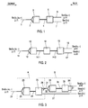
- FIG. 1 shows a block diagram of a demultiplexer according to the invention.
- 1 is a monomodal input channel for an incoming optical signal S i1 ( ⁇ 1, ⁇ 2, ⁇ 3, --) which is composed of optical signal components having wavelengths ⁇ 1, ⁇ 2, ⁇ 3, --, and of which at least the component having the wavelength ⁇ 1 has a defined polarisation, for example TE or TM.
- a taper section 2 passes the monomodal input channel 1 to the bimodal input of a 100%TX00-TY01( ⁇ 1) mode converter 3 which, via a bimodal junction channel 4, is jointed to a mode splitter 5 having a first output channel 6 and a second output channel 7, both monomodal.
- This mode splitter 5 is of a type known per se, such as that disclosed, for example, by reference [4], in particular Figure 2(a), the first output channel having a higher propagation constant than the second. That part of a signal which enters the mode splitter in a zero-order mode via the bimodal intermediate channel 4 will therefore leave this splitter via output channel 6, and that part of a signal which enters the mode splitter in a first-order mode via the bimodal intermediate channel 4 will leave this splitter via output channel 7.
- TX is accordingly the defined polarisation TE or TM.
- the signal S i1 ( ⁇ 1, ⁇ 2, ⁇ 3, --) propagates in the input channel 1, but also in the taper section 2, in zero-order guided modes for all wavelengths.
- the zero-order guided mode of the component having the wavelength ⁇ 1 and the defined polarisation is completely converted into the first-order guided mode having the polarisation TY, while the remaining light continues to propagate in the zero-order mode.
- the optical signal which has entered the mode splitter 5 via the bimodal intermediate channel 4 only the part which propagates in first-order mode is converted into a zero-order guided mode in output channel 7, the output channel having the lowest propagation constant. Conversely, that part of the optical signal which enters the mode splitter 5 in the zero-order mode will leave the mode splitter entirely via the output channel 6 having the highest propagation constant.
- an output signal S o1 ( ⁇ 1) propagating via the output channel 7 will contain all of the ⁇ 1 component from the original incoming optical signal S i1 ( ⁇ 1, ⁇ 2, ⁇ 3, --), in particular, with the polarisation acquired by said component in the converter.
- An output signal S o1 ( ⁇ 2, ⁇ 3, --) propagating via the output channel 6 contains the remaining optical signal, i.e. the original incoming optical signal S i1 ( ⁇ 1, ⁇ 2, ⁇ 3, --) from which the ⁇ 1 component has been removed.
- the mode converter 3 is preferably chosen in such a way that the polarisation TY differs from TX, since in that case additional polarisation filters can be used in the output channels 6 and 7 of the mode splitter 5, in order to increase further the suppression of unwanted wavelength components.
- the ⁇ 1 component in the input signal does not have a defined polarisation, it can propagate both in a TE00 and in a TM00 guided mode.
- a demultiplexer according to Figure 1 having only one mode converter 3 can only split off the ⁇ 1 component having one of the two polarisations, with the result that the ⁇ 1 component having the other polarisation is still present in the output signal which appears on output channel 6.
- two demultiplexer variants are described by means of which this ⁇ 1 component can be removed as well.
- a first way is to incorporate, in addition, a second mode converter which is selective for the ⁇ 1 component having the other polarisation in the bimodal intermediate channel 4 downstream of the first mode converter 3, namely the 100%TX00 ⁇ TY01( ⁇ 1) mode converter 3.
- Figure 2 shows the corresponding block diagram. Components corresponding to the demultiplexer of Figure 1 have a number with the same last figure in the block diagram of Figure 2. Said second mode converter is indicated by 18, and the sections of the intermediate channel 14 on both sides of the mode converter 18 are indicated by 14.1 and 14.2.
- the mode converter 18 is a 100%TW00 ⁇ TZ01( ⁇ 1) mode converter, where TW and TZ denote polarisations which are not equal to TX and TY, respectively.
- a second way is to put two demultiplexers according to the block diagram of Figure 1 in series.
- a block diagram of such an arrangement is shown in Figure 3.
- the components of a first demultiplexer (broken-line box A) are numbered from 21 to 27 inclusive, the correspondence with the components of the demultiplexer according to the block diagram of Figure 1 again being expressed in the last figure.
- the series connection is achieved by jointing the output channel 26 of the first demultiplexer to the input channel 31 of the second demultiplexer at point P.
- the mode converter 23 is a 100%TX00 ⁇ TY01( ⁇ 1) converter.
- the mode converter 33 is a 100%TW00 ⁇ TZ01( ⁇ 1) converter, in which TW, TX, TY and TZ again denote polarisations which may be chosen arbitrarily, obviously, of course, with the restriction that TW and TX must be different.
- An output signal S o31 ( ⁇ 1) on output channel 27 consists of the ⁇ 1 component which propagates with the TX polarisation in the input signal S i3 ( ⁇ 1, ⁇ 2, --).
- the ⁇ 1 component which propagates with the TW polarisation in the input signal S i3 ( ⁇ 1, ⁇ 2, --) remains in the residual signal, which leaves the first demultiplexer via output channel 26 and which enters the second demultiplexer via input channel 31.
- the demultiplexer operates in that case as a completely passive polarisation converter which is independent of the incoming polarisation state.
- Mode converters and mode splitters used in the demultiplexers described above operate in reverse for optical signals with an opposite direction of propagation.
- a mode splitter becomes a combiner
- a 100%TX00 ⁇ TY01( ⁇ 1) converter becomes a 100%TY01 ⁇ TX00( ⁇ 1) converter.
- the output channels (6,7; 16,17; 36,37,27) as input channels for input signals corresponding to the various S o -signals
- the original input signals S i are now obtained as output signals at the original input channels (1; 11; 21), which are now used as output channels.
- the demultiplexers according to the invention operate in the reverse direction, that is to say with signal reversal, as multiplexers and that they can be used as such. This is indicated in the drawing by thick arrows DEMUX and MUX, respectively. In this case, care must be taken in the multiplexers according to the block diagrams of Figure 1 and Figure 3 that signals having the correct polarisations are supplied.
Landscapes
- Physics & Mathematics (AREA)
- General Physics & Mathematics (AREA)
- Optics & Photonics (AREA)
- Engineering & Computer Science (AREA)
- Microelectronics & Electronic Packaging (AREA)
- Optical Integrated Circuits (AREA)
- Optical Communication System (AREA)
- Bending Of Plates, Rods, And Pipes (AREA)
- Control Of Motors That Do Not Use Commutators (AREA)
- Telephone Function (AREA)
- Ultra Sonic Daignosis Equipment (AREA)
- Investigating Or Analyzing Materials By The Use Of Ultrasonic Waves (AREA)
Applications Claiming Priority (2)
| Application Number | Priority Date | Filing Date | Title |
|---|---|---|---|
| NL9101532A NL9101532A (nl) | 1991-09-10 | 1991-09-10 | Golflengte-selectieve multiplexer en demultiplexer. |
| NL9101532 | 1991-09-10 |
Publications (2)
| Publication Number | Publication Date |
|---|---|
| EP0536819A1 true EP0536819A1 (de) | 1993-04-14 |
| EP0536819B1 EP0536819B1 (de) | 1997-03-12 |
Family
ID=19859686
Family Applications (1)
| Application Number | Title | Priority Date | Filing Date |
|---|---|---|---|
| EP92202636A Expired - Lifetime EP0536819B1 (de) | 1991-09-10 | 1992-09-01 | Wellenlängenmultiplexer und Demultiplexer |
Country Status (10)
| Country | Link |
|---|---|
| US (1) | US5325221A (de) |
| EP (1) | EP0536819B1 (de) |
| JP (1) | JP2517517B2 (de) |
| AT (1) | ATE150182T1 (de) |
| CA (1) | CA2077881C (de) |
| DE (1) | DE69218098T2 (de) |
| ES (1) | ES2099790T3 (de) |
| FI (1) | FI106490B (de) |
| NL (1) | NL9101532A (de) |
| NO (1) | NO308497B1 (de) |
Cited By (4)
| Publication number | Priority date | Publication date | Assignee | Title |
|---|---|---|---|---|
| WO1995022070A1 (en) * | 1994-02-11 | 1995-08-17 | Philips Electronics N.V. | Optical device with phased array |
| US5680236A (en) * | 1995-01-02 | 1997-10-21 | Koninklijke Ptt Nederland N.V. | Integrated optical wavelength demultiplexer |
| EP3339922A1 (de) * | 2016-12-23 | 2018-06-27 | Huawei Technologies Co., Ltd. | Optischer chip und verfahren zur kopplung von licht |
| CN111766662A (zh) * | 2020-07-24 | 2020-10-13 | 上海交通大学 | 一种通用型硅基集成光波导模式转换器 |
Families Citing this family (11)
| Publication number | Priority date | Publication date | Assignee | Title |
|---|---|---|---|---|
| NL9200328A (nl) * | 1992-02-21 | 1993-09-16 | Nederland Ptt | Optische schakelcomponent. |
| JPH0720329A (ja) * | 1993-06-23 | 1995-01-24 | Canon Inc | 光合分波器 |
| US5539850A (en) * | 1994-12-30 | 1996-07-23 | At&T Corp. | Polarization and wavelength independent optical waveguide tap |
| US5675675A (en) * | 1995-12-29 | 1997-10-07 | Corning Incorporated | Bandwidth-adjusted wavelength demultiplexer |
| US6018317A (en) * | 1995-06-02 | 2000-01-25 | Trw Inc. | Cochannel signal processing system |
| KR0164113B1 (ko) * | 1995-11-02 | 1998-12-01 | 양승택 | 광 도파로 내의 모드 변환과 모드 선택을 이용한 광교환 장치 |
| FR2742882B1 (fr) * | 1995-12-22 | 1998-02-13 | Corning Inc | Demultiplexeur de longueurs d'onde, realise en optique integree |
| EP0816877A1 (de) * | 1996-07-01 | 1998-01-07 | Corning Incorporated | Multiplexer/Demultiplexer mit flacher spektraler Antwort |
| US5799119A (en) * | 1996-07-03 | 1998-08-25 | Northern Telecom Limited | Coupling of strongly and weakly guiding waveguides for compact integrated mach zehnder modulators |
| US5937113A (en) * | 1998-04-17 | 1999-08-10 | National Research Council Of Canada | Optical grating-based device having a slab waveguide polarization compensating region |
| US6834187B1 (en) | 2002-09-05 | 2004-12-21 | Agilent Technologies, Inc. | Method of devising a frequency plan for a signal analysis circuit |
Family Cites Families (10)
| Publication number | Priority date | Publication date | Assignee | Title |
|---|---|---|---|---|
| US4390236A (en) * | 1981-03-19 | 1983-06-28 | Bell Telephone Laboratories, Incorporated | Tunable polarization independent wavelength filter |
| US4768851A (en) * | 1983-11-30 | 1988-09-06 | The Board Of Trustees Of The Leland Stanford Junior University | Fiber optic modal coupler, interferometer and method of coupling spatial modes using same |
| DE3406207A1 (de) * | 1984-02-21 | 1985-08-29 | Philips Patentverwaltung Gmbh, 2000 Hamburg | Integriert-optische wellenlaengenmultiplex- und -demultiplexeinrichtung fuer monomode-uebertragungssysteme und ihre verwendung |
| US4606605A (en) * | 1984-06-29 | 1986-08-19 | At&T Bell Laboratories | Optical fiber having in-line polarization filter |
| US4906064A (en) * | 1988-12-30 | 1990-03-06 | Bell Communications Research, Inc. | Switch for selectively switching optical wavelengths |
| ATE139387T1 (de) * | 1989-03-31 | 1996-06-15 | Sel Alcatel Ag | Optisches nachrichtenübertragungssystem zur diplex- oder duplex-übertragung |
| US5009477A (en) * | 1989-05-12 | 1991-04-23 | At&T Bell Laboratories | Optical interconnect arrangement |
| US5121450A (en) * | 1989-12-22 | 1992-06-09 | Gte Laboratories Incorporated | Fiber optical Y-junction |
| US5093876A (en) * | 1990-07-27 | 1992-03-03 | At&T Bell Laboratories | WDM systems incorporating adiabatic reflection filters |
| NL9100852A (nl) * | 1991-05-16 | 1992-12-16 | Nederland Ptt | Modusomzetter. |
-
1991
- 1991-09-10 NL NL9101532A patent/NL9101532A/nl not_active Application Discontinuation
-
1992
- 1992-09-01 AT AT92202636T patent/ATE150182T1/de not_active IP Right Cessation
- 1992-09-01 DE DE69218098T patent/DE69218098T2/de not_active Expired - Fee Related
- 1992-09-01 EP EP92202636A patent/EP0536819B1/de not_active Expired - Lifetime
- 1992-09-01 ES ES92202636T patent/ES2099790T3/es not_active Expired - Lifetime
- 1992-09-02 NO NO923426A patent/NO308497B1/no not_active IP Right Cessation
- 1992-09-08 JP JP4280407A patent/JP2517517B2/ja not_active Expired - Fee Related
- 1992-09-08 US US07/941,402 patent/US5325221A/en not_active Expired - Fee Related
- 1992-09-09 CA CA002077881A patent/CA2077881C/en not_active Expired - Fee Related
- 1992-09-10 FI FI924057A patent/FI106490B/fi active
Non-Patent Citations (3)
| Title |
|---|
| IEEE JOURNAL OF QUANTUM ELECTRONICS vol. QE-11, no. 1, January 1975, NEW YORK US pages 32 - 39 W.K. BURNS AND A.F. MILTON 'Mode Conversion in Planar-Dielectric Separating Waveguides' * |
| IEEE PHOTONICS TECHNOLOGY LETTERS vol. 2, no. 7, June 1990, NEW YORK, US pages 484 - 486 K. O. HILL ET AL. 'A Novel Low-Loss Inline Bimodal-Fiber Tap: Wavelength-Selective Properties' * |
| SPIE Vol. 993 Integrated optical Circuit Engineering VI (1988), invited paper, T. MIYASHITA et al. : 'Integrated optical devices based on silica waveguide technologie', page 288-294 * |
Cited By (6)
| Publication number | Priority date | Publication date | Assignee | Title |
|---|---|---|---|---|
| WO1995022070A1 (en) * | 1994-02-11 | 1995-08-17 | Philips Electronics N.V. | Optical device with phased array |
| US5680236A (en) * | 1995-01-02 | 1997-10-21 | Koninklijke Ptt Nederland N.V. | Integrated optical wavelength demultiplexer |
| EP3339922A1 (de) * | 2016-12-23 | 2018-06-27 | Huawei Technologies Co., Ltd. | Optischer chip und verfahren zur kopplung von licht |
| US10578806B2 (en) | 2016-12-23 | 2020-03-03 | Huawei Technologies Co., Ltd. | Optical chip and method for coupling light |
| CN111766662A (zh) * | 2020-07-24 | 2020-10-13 | 上海交通大学 | 一种通用型硅基集成光波导模式转换器 |
| CN111766662B (zh) * | 2020-07-24 | 2021-09-07 | 上海交通大学 | 一种通用型硅基集成光波导模式转换器 |
Also Published As
| Publication number | Publication date |
|---|---|
| JPH05235901A (ja) | 1993-09-10 |
| NO308497B1 (no) | 2000-09-18 |
| JP2517517B2 (ja) | 1996-07-24 |
| EP0536819B1 (de) | 1997-03-12 |
| NL9101532A (nl) | 1993-04-01 |
| CA2077881C (en) | 1997-02-25 |
| ES2099790T3 (es) | 1997-06-01 |
| CA2077881A1 (en) | 1993-03-11 |
| NO923426L (no) | 1993-03-11 |
| FI924057A0 (fi) | 1992-09-10 |
| ATE150182T1 (de) | 1997-03-15 |
| FI924057A7 (fi) | 1993-03-11 |
| NO923426D0 (no) | 1992-09-02 |
| DE69218098D1 (de) | 1997-04-17 |
| US5325221A (en) | 1994-06-28 |
| DE69218098T2 (de) | 1997-08-07 |
| FI106490B (fi) | 2001-02-15 |
Similar Documents
| Publication | Publication Date | Title |
|---|---|---|
| US11714238B2 (en) | Wavelength division multiplexing filter for multiplexing or demultiplexing using cascaded frequency shaping | |
| JP2545047B2 (ja) | 光通信ネットワ―クにおける光搬送波抽出,再挿入機器 | |
| EP0536819B1 (de) | Wellenlängenmultiplexer und Demultiplexer | |
| US5473719A (en) | Optical dispersion compensator | |
| JP3448182B2 (ja) | 全光ファイバ製光ルータ | |
| US6839482B2 (en) | Tunable optical filtering device and method | |
| EP3800491A1 (de) | Optische multiplexer-schaltung | |
| US6256433B1 (en) | Expandable interleaving optical add/drop filter module | |
| KR960008352A (ko) | 광학 장치 | |
| JPH10221560A (ja) | 光波長フィルタ及び光デマルチプレクサ | |
| EP0649040B1 (de) | Optischer Bandpass-Filter | |
| US6885823B2 (en) | Wavelength multiplexing/demultiplexing unit, wavelength multiplexing/demultiplexing apparatus and wavelength multiplexing/demultiplexing method | |
| EP0818897B1 (de) | Lichtverzweiger- und Lichtinsertionsgerät und optisches Übertragungssystem mit einem Lichtverzweiger- und Lichtinsertionsgerät | |
| US6600852B1 (en) | Wavelength selective device and switch and method thereby | |
| EP1266471B1 (de) | Einrichtung und verfahren zum optischen add/drop-multiplexen | |
| JPS60172841A (ja) | 光スイツチ | |
| EP1122905A2 (de) | Vorrichtung und Verfahren zum Wellenlängenmultiplexen und -demultiplexen | |
| JP2002072008A (ja) | 光分波器および光合波器 | |
| KR100280831B1 (ko) | 초고속광신호의파장분할광다중/역다중기 | |
| JPH01187537A (ja) | 波長変換スイッチ | |
| Yun et al. | Design of wavelength-selective directional coupler made of W-index waveguide for WDM | |
| JPH06347656A (ja) | 光回路 | |
| JP2003315574A (ja) | 光合分波器 |
Legal Events
| Date | Code | Title | Description |
|---|---|---|---|
| PUAI | Public reference made under article 153(3) epc to a published international application that has entered the european phase |
Free format text: ORIGINAL CODE: 0009012 |
|
| AK | Designated contracting states |
Kind code of ref document: A1 Designated state(s): AT BE CH DE DK ES FR GB GR IT LI LU NL PT SE |
|
| 17P | Request for examination filed |
Effective date: 19930908 |
|
| 17Q | First examination report despatched |
Effective date: 19950504 |
|
| GRAG | Despatch of communication of intention to grant |
Free format text: ORIGINAL CODE: EPIDOS AGRA |
|
| GRAH | Despatch of communication of intention to grant a patent |
Free format text: ORIGINAL CODE: EPIDOS IGRA |
|
| GRAH | Despatch of communication of intention to grant a patent |
Free format text: ORIGINAL CODE: EPIDOS IGRA |
|
| GRAA | (expected) grant |
Free format text: ORIGINAL CODE: 0009210 |
|
| AK | Designated contracting states |
Kind code of ref document: B1 Designated state(s): AT BE CH DE DK ES FR GB GR IT LI LU NL PT SE |
|
| PG25 | Lapsed in a contracting state [announced via postgrant information from national office to epo] |
Ref country code: GR Free format text: LAPSE BECAUSE OF FAILURE TO SUBMIT A TRANSLATION OF THE DESCRIPTION OR TO PAY THE FEE WITHIN THE PRESCRIBED TIME-LIMIT Effective date: 19970312 Ref country code: DK Effective date: 19970312 |
|
| REF | Corresponds to: |
Ref document number: 150182 Country of ref document: AT Date of ref document: 19970315 Kind code of ref document: T |
|
| REG | Reference to a national code |
Ref country code: CH Ref legal event code: NV Representative=s name: ISLER & PEDRAZZINI AG Ref country code: CH Ref legal event code: EP |
|
| REF | Corresponds to: |
Ref document number: 69218098 Country of ref document: DE Date of ref document: 19970417 |
|
| ITF | It: translation for a ep patent filed | ||
| REG | Reference to a national code |
Ref country code: ES Ref legal event code: FG2A Ref document number: 2099790 Country of ref document: ES Kind code of ref document: T3 |
|
| PG25 | Lapsed in a contracting state [announced via postgrant information from national office to epo] |
Ref country code: PT Effective date: 19970612 |
|
| ET | Fr: translation filed | ||
| PLBE | No opposition filed within time limit |
Free format text: ORIGINAL CODE: 0009261 |
|
| 26N | No opposition filed | ||
| REG | Reference to a national code |
Ref country code: CH Ref legal event code: PFA Free format text: KONINKLIJKE PTT NEDERLAND N.V. TRANSFER- KONINKLIJKE KPN N.V. |
|
| REG | Reference to a national code |
Ref country code: GB Ref legal event code: IF02 |
|
| PGFP | Annual fee paid to national office [announced via postgrant information from national office to epo] |
Ref country code: CH Payment date: 20020816 Year of fee payment: 11 |
|
| PGFP | Annual fee paid to national office [announced via postgrant information from national office to epo] |
Ref country code: NL Payment date: 20020827 Year of fee payment: 11 Ref country code: AT Payment date: 20020827 Year of fee payment: 11 |
|
| PGFP | Annual fee paid to national office [announced via postgrant information from national office to epo] |
Ref country code: LU Payment date: 20020828 Year of fee payment: 11 |
|
| PGFP | Annual fee paid to national office [announced via postgrant information from national office to epo] |
Ref country code: SE Payment date: 20020829 Year of fee payment: 11 |
|
| PGFP | Annual fee paid to national office [announced via postgrant information from national office to epo] |
Ref country code: BE Payment date: 20020913 Year of fee payment: 11 |
|
| PGFP | Annual fee paid to national office [announced via postgrant information from national office to epo] |
Ref country code: ES Payment date: 20020923 Year of fee payment: 11 |
|
| PGFP | Annual fee paid to national office [announced via postgrant information from national office to epo] |
Ref country code: GB Payment date: 20030827 Year of fee payment: 12 |
|
| PG25 | Lapsed in a contracting state [announced via postgrant information from national office to epo] |
Ref country code: LU Free format text: LAPSE BECAUSE OF NON-PAYMENT OF DUE FEES Effective date: 20030901 Ref country code: AT Free format text: LAPSE BECAUSE OF NON-PAYMENT OF DUE FEES Effective date: 20030901 |
|
| PG25 | Lapsed in a contracting state [announced via postgrant information from national office to epo] |
Ref country code: SE Free format text: LAPSE BECAUSE OF NON-PAYMENT OF DUE FEES Effective date: 20030902 Ref country code: ES Free format text: LAPSE BECAUSE OF NON-PAYMENT OF DUE FEES Effective date: 20030902 |
|
| PGFP | Annual fee paid to national office [announced via postgrant information from national office to epo] |
Ref country code: DE Payment date: 20030903 Year of fee payment: 12 |
|
| PGFP | Annual fee paid to national office [announced via postgrant information from national office to epo] |
Ref country code: FR Payment date: 20030904 Year of fee payment: 12 |
|
| PG25 | Lapsed in a contracting state [announced via postgrant information from national office to epo] |
Ref country code: LI Free format text: LAPSE BECAUSE OF NON-PAYMENT OF DUE FEES Effective date: 20030930 Ref country code: CH Free format text: LAPSE BECAUSE OF NON-PAYMENT OF DUE FEES Effective date: 20030930 Ref country code: BE Free format text: LAPSE BECAUSE OF NON-PAYMENT OF DUE FEES Effective date: 20030930 |
|
| BERE | Be: lapsed |
Owner name: KONINKLIJKE *PTT NEDERLAND N.V. Effective date: 20030930 |
|
| PG25 | Lapsed in a contracting state [announced via postgrant information from national office to epo] |
Ref country code: NL Free format text: LAPSE BECAUSE OF NON-PAYMENT OF DUE FEES Effective date: 20040401 |
|
| EUG | Se: european patent has lapsed | ||
| REG | Reference to a national code |
Ref country code: CH Ref legal event code: PL |
|
| NLV4 | Nl: lapsed or anulled due to non-payment of the annual fee |
Effective date: 20040401 |
|
| PG25 | Lapsed in a contracting state [announced via postgrant information from national office to epo] |
Ref country code: GB Free format text: LAPSE BECAUSE OF NON-PAYMENT OF DUE FEES Effective date: 20040901 |
|
| REG | Reference to a national code |
Ref country code: ES Ref legal event code: FD2A Effective date: 20030902 |
|
| PG25 | Lapsed in a contracting state [announced via postgrant information from national office to epo] |
Ref country code: DE Free format text: LAPSE BECAUSE OF NON-PAYMENT OF DUE FEES Effective date: 20050401 |
|
| GBPC | Gb: european patent ceased through non-payment of renewal fee |
Effective date: 20040901 |
|
| PG25 | Lapsed in a contracting state [announced via postgrant information from national office to epo] |
Ref country code: FR Free format text: LAPSE BECAUSE OF NON-PAYMENT OF DUE FEES Effective date: 20050531 |
|
| REG | Reference to a national code |
Ref country code: FR Ref legal event code: ST |
|
| PG25 | Lapsed in a contracting state [announced via postgrant information from national office to epo] |
Ref country code: IT Free format text: LAPSE BECAUSE OF NON-PAYMENT OF DUE FEES;WARNING: LAPSES OF ITALIAN PATENTS WITH EFFECTIVE DATE BEFORE 2007 MAY HAVE OCCURRED AT ANY TIME BEFORE 2007. THE CORRECT EFFECTIVE DATE MAY BE DIFFERENT FROM THE ONE RECORDED. Effective date: 20050901 |