EP0536886B1 - Hochfrequenzenergieversorgungsvorrichtung für eine Leuchtstoffröhre mit Neonblasen- und Quecksilberwanderungsunterdrückung - Google Patents
Hochfrequenzenergieversorgungsvorrichtung für eine Leuchtstoffröhre mit Neonblasen- und Quecksilberwanderungsunterdrückung Download PDFInfo
- Publication number
- EP0536886B1 EP0536886B1 EP92307743A EP92307743A EP0536886B1 EP 0536886 B1 EP0536886 B1 EP 0536886B1 EP 92307743 A EP92307743 A EP 92307743A EP 92307743 A EP92307743 A EP 92307743A EP 0536886 B1 EP0536886 B1 EP 0536886B1
- Authority
- EP
- European Patent Office
- Prior art keywords
- oscillator
- power supply
- neon
- transformer
- high frequency
- Prior art date
- Legal status (The legal status is an assumption and is not a legal conclusion. Google has not performed a legal analysis and makes no representation as to the accuracy of the status listed.)
- Expired - Lifetime
Links
Images


Classifications
-
- H—ELECTRICITY
- H05—ELECTRIC TECHNIQUES NOT OTHERWISE PROVIDED FOR
- H05B—ELECTRIC HEATING; ELECTRIC LIGHT SOURCES NOT OTHERWISE PROVIDED FOR; CIRCUIT ARRANGEMENTS FOR ELECTRIC LIGHT SOURCES, IN GENERAL
- H05B41/00—Circuit arrangements or apparatus for igniting or operating discharge lamps
- H05B41/14—Circuit arrangements
- H05B41/26—Circuit arrangements in which the lamp is fed by power derived from DC by means of a converter, e.g. by high-voltage DC
- H05B41/28—Circuit arrangements in which the lamp is fed by power derived from DC by means of a converter, e.g. by high-voltage DC using static converters
- H05B41/282—Circuit arrangements in which the lamp is fed by power derived from DC by means of a converter, e.g. by high-voltage DC using static converters with semiconductor devices
- H05B41/285—Arrangements for protecting lamps or circuits against abnormal operating conditions
- H05B41/2858—Arrangements for protecting lamps or circuits against abnormal operating conditions for protecting the lamp against abnormal operating conditions
-
- Y—GENERAL TAGGING OF NEW TECHNOLOGICAL DEVELOPMENTS; GENERAL TAGGING OF CROSS-SECTIONAL TECHNOLOGIES SPANNING OVER SEVERAL SECTIONS OF THE IPC; TECHNICAL SUBJECTS COVERED BY FORMER USPC CROSS-REFERENCE ART COLLECTIONS [XRACs] AND DIGESTS
- Y10—TECHNICAL SUBJECTS COVERED BY FORMER USPC
- Y10S—TECHNICAL SUBJECTS COVERED BY FORMER USPC CROSS-REFERENCE ART COLLECTIONS [XRACs] AND DIGESTS
- Y10S315/00—Electric lamp and discharge devices: systems
- Y10S315/05—Starting and operating circuit for fluorescent lamp
-
- Y—GENERAL TAGGING OF NEW TECHNOLOGICAL DEVELOPMENTS; GENERAL TAGGING OF CROSS-SECTIONAL TECHNOLOGIES SPANNING OVER SEVERAL SECTIONS OF THE IPC; TECHNICAL SUBJECTS COVERED BY FORMER USPC CROSS-REFERENCE ART COLLECTIONS [XRACs] AND DIGESTS
- Y10—TECHNICAL SUBJECTS COVERED BY FORMER USPC
- Y10S—TECHNICAL SUBJECTS COVERED BY FORMER USPC CROSS-REFERENCE ART COLLECTIONS [XRACs] AND DIGESTS
- Y10S315/00—Electric lamp and discharge devices: systems
- Y10S315/07—Starting and control circuits for gas discharge lamp using transistors
Definitions
- the present invention relates to high frequency power supplies for use with luminous tubular glass signage of the type often found in connection with retail advertising and decorating. More particularly, the present invention is specifically designed to power luminous tube signage of either the neon or mercury gas variety or, as is often the practice, signs having luminous tube segments of both gas types.
- luminous tube signs (generally referred to generically as "neon signs" regardless of the actual gas employed), were uniformly powered by relatively massive low frequency (e.g. 60 Hz) high-voltage transformers, such transformers being both large and heavy.
- relatively massive low frequency (e.g. 60 Hz) high-voltage transformers such transformers being both large and heavy.
- High frequency power supplies offer significant reductions in both size and weight as compared to this older low frequency transformer technology. But not unexpectedly, there are inevitable trade-offs - - in the present case, the concomitant liabilities of "neon bubble formation” and “mercury atom migration", problems uniquely associated with high frequency excited luminous tubes.
- mercury is an equally common gas used in so-called “neon” signage.
- neon is only used in those signs, or those portions of signs, in which the 'warm'colors of red, orange, pink and some shades of purple are desired.
- cool' colors are intended, e.g. blue, turquoise and white, mercury is employed.
- the visible spectral radiation of mercury may be employed directly as the visible medium or, as commonly, the ultraviolet radiation of mercury may be used in an indirect manner to excite phosphor coatings as required to produce the desired colors. It is significant to the present invention that many signs employ both neon and mercury luminous tube segments. It is therefore necessary that the present high frequency supply properly excite luminous tubes of either or both gas types.
- Neon for example, remains a gas at room temperature while mercury is a liquid of low vapor pressure. Neon is relatively inert and therefore does not form chemical compounds.
- Mercury by contrast, is very reactive and may combine with oxygen in the air to form, for example, various solid oxides.
- Neon does not suffer from the ion/atom migration problem and therefore there is no corresponding restriction against the use of DC or non-symmetric AC power supply waveforms. Neon, however, has its own unique problem of bubble formation. Indeed, as discussed in U.S. Patent No. 4,862,042 to Herrick, this phenomenon is well known and, in the cited reference, the deliberate introduction of DC currents is exploited to produce certain selected visually desirable effects associated with bubble formation and controlled movement of the bubbles within the neon tube.
- the present invention seeks to simultaneously eliminate both the mercury migration and neon bubble formation problems thereby resulting in a high frequency supply that may be interchangeably used with tubes of either construction or, more commonly, with signs having tube segments of both gas types.
- the present invention provides a high frequency power supply for neon and mercury gas tube loads including a high frequency transformer having primary and high-voltage secondary windings, means for connecting the secondary winding to a gas tube load for passing a current therethrough; DC input means for connection to a source of DC power; switch means connected to the DC input means and to the primary of the transformer for connecting the DC input means to the transformer primary and for selectively reversing the polarity of the input from the DC input means to the transformer primary; controller means operatively connected to the switch means for effecting the polarity switching of the switch means; characterized in that the controller means includes means for generating a first higher frequency asymmetric signal and means for generating a second lower frequency symmetric signal; means for combining the first asymmetric and second symmetric signals to produce a composite signal having an asymmetrical higher frequency waveform, the phase of the asymmetry being reversed symmetrically at the lower frequency rate whereby the current through a gas tube load is at all times asymmetrical but where the long-term current wave
- the present invention relies on the discovery that the respective problems exhibit dissimilar time constants, that is, mercury migration generally requires a period of hours if not weeks or months to develop while neon bubble formation occurs substantially instantaneously.
- the present invention seeks to produce a DC or asymmetrical component of sufficient duration to visually defeat bubble formation while simultaneously assuring no long-term DC or asymmetrical component.
- a zero DC component non-symmetrical waveform is generated with the asymmetry of this waveform being automatically and periodically reversed.
- the applied waveform remains continuously non-symmetrical thereby assuring bubble invisibility while the long-term symmetry afforded by the periodically reversing asymmetry minimizes or eliminates all mercury migration.
- the arrangement proposed achieves this result at minimal circuity complexity and expense, specifically, by causing the requisite reversal within the low voltage driver portion of the supply thereby eliminating any relays or other high voltage switching components.
- a DC biased symmetrical AC waveform in which the sense or polarity of the DC bias is, again, reversed at an appropriate long-term periodical rate.
- the preferred embodiment employs a square -wave reversal of the DC bias.
- waveforms such as sine waveforms
- the present approach minimizes circuit complexity by avoiding the bulk and cost of, for example, additional 60Hz transformers or windings and, further, provides better bubble elimination.
- the zero-crossing points of non-square wave DC bias reversal sources define partial bubble formation regions with correspondingly poorer bubble suppression capabilities.
- the preferred arrangement seeks to employ the series current fed push-pull resonant oscillator which is well known in the fluorescent ballast industry.
- the oscillator output incorporates a leakage reactance output step-up transformer which, in turn, drives the neon or mercury load.
- the present invention therefore seeks to implement the low cost series current fed oscillator through employment of a novel parasitic oscillation suppression arrangement.
- a second winding is positioned and coupled to the series current feed choke and energy, related only to the parasitic oscillation, is coupled, rectified, and returned to the DC power source in a manner that both suppresses the unwanted oscillation but without the normal power losses associated with known suppression schemes.
- a further feature of the present reversing DC current migration/bubble elimination high frequency oscillator is that of the output DC current switching circuitry. While it is generally known that residual DC tube currents cause mercury migration, and that the reversal of such currents minimize this migration, known current reversing arrangements have not been totally satisfactory, either due to cost or circuit efficacy. As noted above, for example, use of a series connected 60 Hz transformer is not believed to fully quench bubble formation and, in any event, is contrary to the underlying objectives associated with high frequency power supplies in its re-introduction of a relatively bulky 60 Hz transformer.
- DC current reversal is achieved through the switching of a diode element in alternate polarities across a reactance element in series with the reactance transformer output.
- the diode serves to shunt the reactance for current flow through the secondary in one direction only thereby generating the previously noted DC off-set current.
- the present invention avoids the complexity and costs associated with multiple switching devices and diode elements ordinarily required to implement the required reactance polarity switching.
- an arrangement of two FET devices provides both the switching and diode functions by advantageously employing an intrinsic diode defined within the FET structure when the FET is in the off condition.
- each FET alternately performs a switching and a diode current shunting function thereby resulting in a high performance mercury migration elimination circuit of minimum cost, complexity, and of corresponding increased reliability.
- Such supply should eliminate or minimize the formation of visible bubbles in neon tube segments and the migration of gas atoms in mercury tube segments thereby providing a efficacious high frequency power source suitable for exciting composite neon/mercury gas signs for substantially unlimited time periods.
- a further and important object is that such supply must be cost effective and reliable and consequently should avoid the use of additional and bulky 60Hz transformers or windings and/or high voltage relays or similar switching devices.
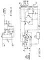
- Figure 1 illustrates a first embodiment 10 of the mercury migration and neon bubble elimination high frequency power supply of the present invention.
- Supply 10 is connected to a source of alternating current at 12 from, for example, standard 120 volt, 50/60Hz power mains.
- This AC power is, in turn, rectified and filtered at 14 in a conventional manner to provide a source of DC, typically about 160 volts, to operate the high frequency oscillator and other components described hereinafter.
- Ground fault circuitry includes a ground fault current detector and timer 16 and a switch 18 to interrupt or disconnect rectifier 14 power from the high frequency oscillator circuitry which, in turn, causes secession of all output voltage and current to the gas tube load.
- the rectified DC voltage, as passed by switch 18 , is connected to, and supplies the operating power required by, the series current-fed oscillator 20 .
- Oscillator 20 operates with a resonant output, the inductive component of which is provided by output transformer 22 .
- Transformer 22 is of the leakage reactance type and includes, as described in more detail below, a pair of series-connected secondary windings which are, in turn, connected to the neon and/or mercury gas tube load 24 .
- a suppressor 26 is integrally incorporated into oscillator 20 to eliminate low frequency parasitic oscillations otherwise found to occur. Suppressor 26 is described in more detail below.
- the symmetrical DC current reverser 28 which, when interfaced with the above-noted pair of transformer 22 secondary windings, provides the required DC anti-bubble bias with periodic anti-migration phase reversal.
- FIG. 2 is an explanatory schematic diagram illustrating operation of the symmetrical DC current reverser 28 as well as its interconnection to reactance transformer 22 .
- Transformer 22 incorporates generally conventional primary and feedback windings 30 and 32 , respectively, and, as noted, a pair of secondary windings 34 and 36 . These output windings are generally in a series-aiding configuration with the summed output thereof being connected to the neon/mercury gas tube 24 .
- the respective center leads 38 and 40 of these windings are not directly connected, but are interconnected through current reverser 28 shown within the dotted line of Figure 2.
- Reverser 28 comprises a reactive element 42 , preferably a capacitor, placed in series with windings 34 and 36 and a pair of opposed, series-connected diodes 44 and 46 across capacitor 42 .
- Reverser 28 operates by alternately shunting one of the diodes 44 and 46 which, in turn, places the remaining, non-shunted diode electrically across capacitor 42 .
- Electronic switches 48 and 50 are placed across respective diodes 44 and 46 and are synchronously driven by a low frequency clock 52 .
- Clock 52 may be of any convenient configuration and should have a frequency generally well-below that of the high frequency oscillator 20 , the latter frequency typically being in the order of 20 Khz.
- the switch clocking signal is derived from the AC line input 12 ( Figure 1) and is therefore 50/60 Hz.
- An invertor 54 between the respective gate inputs of switches 48 and 50 assures that one switch, and only one switch, will be closed at any given instant, in turn, guaranteeing that one diode will electrically he in shunt across the capacitor at all times.
- the effect of placing a diode across capacitor 42 is to create a low impedance current path for that half output cycle for which current is flowing in the direction of the diode and a higher impedance current path - - increased by the reactance of the capacitor - - for the half output cycle for which current is forced to flow contrary to the diode, that is, where the current must flow through capacitor 42 .
- the resulting asymmetrical output current flow constitutes the superposition of symmetrical AC and quiescent DC current waveforms.
- Figure 2 is merely illustrative of circuit operation.
- Figure 3 represents the actual circuit topology of the preferred embodiment in which a pair of insulated gate FETs 56 and 58 are advantageously employed in the actual capacity as electronic switches and capacitor shunt diodes.
- FET 58 performs the function of, and replaces, both the diode 44 and switch 48 (of Figure 2).
- FET 56 serves as the invertor 54 of Figure 2 required to drive FET switch 58 .
- Resistors 51 and 53 couple the inverted output of FET 56 to the gate input of FET 58 .
- diode 46 and switch 50 are replaced by FET 58 .
- Zener diodes 55 and 57 protect the respective gate-source junctions against over-voltage. Twelve volt zeners are appropriate.
- Capacitors 59 and 61 serve to by-pass the gates of FET 56 and 58 for the high frequencies generated by oscillator 20 . It will be appreciated that this dual and triple (in the case of FET 57) functionality represents a meaningful improvement in circuit simplicity with its corresponding improvement in reliability and reduction in cost.
- FIG. 4 is the schematic representation of the series current-fed oscillator 20 including output reactance transformer 22 and parasitic oscillation suppressor 26 .
- Oscillator 20 is of generally conventional configuration and will not be discussed further herein except to note that the input choke required by such oscillators has been replaced by transformer 60 having primary and secondary windings 62 and 64 , respectively.
- suppressor 26 ( Figure 1) may best be understood by reference to the waveform diagrams of Figures 5 and 6. These diagrams depict the voltage waveform present at the output end 66 ( Figure 4) of series-fed oscillator input choke 62 .
- choke 62 comprises the primary winding of transformer 60 .
- Figure 6 illustrates the desired waveform of a series-fed oscillator.
- Figure 5 illustrates the waveform of a series-fed oscillator exhibiting an undesired low frequency parasitic oscillation condition.
- parasitic oscillations have been found in series-fed power supplies employing a reactance output transformer, such as transformer 22 , and powering a neon gas tube, for example, neon load 24 .
- the peak voltages caused by such oscillations often exceed the maximum ratings of the oscillator transistors and, in any event, result in an objectionable, audible whining or squealing noise.
- the peak voltage is approximately 1.57V dc .
- the secondary 64 of transformer 60 is connected in series with resistor 68 and diode 70 , the combination of this series configuration being connected across the power supply input of voltage, V dc . It will be observed that the polarity of diode 70 is such that any current flow through this diode, that is, any energy recovered by the parasitic oscillation suppressor 26 will be returned as useful power to the supply thereby effecting suppression without undue lost power dissipation.
- Figure 7 illustrates the desired waveform appearing across the secondary 64 of transformer 60 during normal oscillator operation (i.e. without any parasitic oscillation).
- V dc peak positive voltage
- V dc peak positive voltage
- Resistor 68 should be approximately equal to the input impedance of the series-fed oscillator at full load, although proper operation will be found over a wide range of values down to as low as 10 % of the input impedance. For a 120 VAC power supply, the optimum value is about 150 ohms.
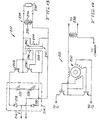
- Figure 8 is a block illustration of a second embodiment of the anti-migration/anti-bubble high frequency power supply 110 of the present invention in which no DC off-set bias is employed. Rather, an asymmetrical current is applied to the primary of the high voltage output transformer thereby eliminating neon bubble formation while the phase of this non-symmetrical input current is periodically reversed, at a relatively lower rate, to minimize or eliminate mercury migration.
- supply 110 is connected to a source of 120/240 volt, 50/60Hz AC mains 112 which, in turn, are connected to rectifier/filter 116 through an EMI (electromagnetic interference) filter 114 .
- the DC output from rectifier/filter 116 is preferably about 360 V dc .
- a half-bridge polarity reversing switcher 118 connects the DC supply voltage to the primary of output transformer 120 , the output of which is connected to the neon/mercury gas tube load 122 .
- Switcher 118 periodically reverses the current through the primary of output transformer 120 in accordance with switching signals generated by controller 124 .
- controller 124 includes a pair of oscillators 126 and 128 , the outputs of which form inputs to exclusive-OR gate 130 .
- Oscillator 126 is of comparatively high frequency (e.g. about 25 KHz) and of non-symmetric output waveform while oscillator 128 provides a symmetric low frequency output preferably in the order of about 1 Hz.
- These oscillators may be of conventional design with the lower frequency oscillator being free-running or, advantageously, being derived by digitally dividing the higher frequency oscillator output.
- Figures 9 and 10 illustrate the output signals generated by respective oscillators 126 and 128 .
- Figure 11 depicts the combination of the oscillator signals as the combination appears at the output 132 of, exclusive-OR gate 130 .
- Gate 130 output is, in turn, inverted at 134 thereby providing complementary input signals 136 and 138 to switch driver 140 .
- An International Rectifier IR-2110 integrated driver may be employed.
- driver 140 includes complementary outputs 142 and 144 which, in turn, alternately gate respective current switches 146 and 148 "on” and “off” in conventional half-bridge fashion. In operation, the complementary outputs from driver 140 assure that only one of the switches will be “closed” or "on” at any given instant.
- Switches 146 or 148 are preferably FETs, for example, International Rectifier, IRF-830.
- Figures 13 and 14 illustrate two alternate arrangements 210 and 212, respectively, for achieving the symmetrically switched asymmetrical luminous tube current of the present invention. These embodiments, respectively, represent parallel and series saturable reactor feedback oscillator implementations to achieve the periodically (symmetrically) reversing asymmetrical luminous tube current function.
- Capacitors 222 and 226 are not conventional, however. The capacitance of these capacitors is undersized, that is, well below the nominal capacitance required to effect full filtering. In fact, capacitance values are selected to insure substantial ripple, such as depicted in Figure 15.
- supply 210 includes a pair of push-pull switching transistors 228 and 230 connected to the primary 232 of output transformer 234 , the secondary 236 of which is connected to the neon/mercury luminous gas tube load 238 .
- a second transformer 240 having a saturable core 242 , is employed in the oscillator feedback path.
- the primary 244 of feedback transformer 240 is placed in parallel with the output transformer 234 while a pair of secondary windings 246 and 248 are provided, each connected to a base input of respective transistors 228 , 230.
- oscillator 210 Operation of oscillator 210 is best understood by reference to Figures 13 and 15. At time t 0 the voltage across capacitor C 1 is maximum while the voltage across capacitor C 2 is near minimum. Thus, during those half-cycles (i.e. high frequency cycles, remembering that oscillator 210 is essentially a high frequency oscillator operating at approximately 25 Khz) in which transistor 228 is turned-on, i.e. saturated, and transistor 230 is turned-off, i.e. cut-off, significantly more voltage will be placed across the primary of output and feedback transformers 234 and 240 than during the corresponding opposite half-cycles in which transistors 228 and 230 are "off" and "on", respectively.
- half-cycles i.e. high frequency cycles, remembering that oscillator 210 is essentially a high frequency oscillator operating at approximately 25 Khz
- transistor 230 is turned-off, i.e. cut-off
- transformer 240 is of the saturable core variety, being selected to saturate during each high frequency half cycle. Until saturation occurs, transformer 240 functions in the normal manner, that is, voltages are induced in the secondary windings which serve to bias one of the oscillator transistors "on” while the other is “off". Once saturation is reached, however, no further base drive is available to the "on” transistor thereby forcing turn-off of that device. The resulting magnetic field collapse induces an opposite polarity voltage in the secondary windings 246 and 248 thereby turning "on” the second transistor which remains on until core saturation is again achieved. In this manner oscillation is sustained.
- the specific time required to force each core saturation cycle depends on the voltage across the primary 244 of the transformer which, in part, is a function of which transistor is turned “on”. As noted, at time t 0 the voltage across the primary of transformer 240 is greater during the positive half-cycles ( i.e. transistor 228 is “on") than during the negative half-cycles ( i.e. transistor 230 is “on”) thereby causing a correspondingly more rapid turn-off of transistor 228 than transistor 230 . In this manner, an asymmetrical high frequency waveform is generated which, as discussed, results in the visible disappearance of neon bubbles.
- Figure 14 illustrates an alternative arrangement for the above-described saturable core symmetrically reversing asymmetrical oscillator in which the configuration of the saturable core feedback transformer 240 is changed from parallel configuration depicted in Figure 13 to a series configuration as shown at 250 in Figure 14.
- the operation of the oscillators of Figures 13 and 14 are otherwise the same.
Landscapes
- Circuit Arrangements For Discharge Lamps (AREA)
- Vessels And Coating Films For Discharge Lamps (AREA)
- Discharge Lamps And Accessories Thereof (AREA)
Claims (11)
- Hochfrequenznetzgerät für Neon- und Quecksilber-Gasröhrenlasten, welches aufweist:- einen Hochfrequenztransformator (120, 234), welcher Primär- (150, 232) und Hochspannungs-Sekundärwicklungen (236) aufweist;- ein Mittel für die Verbindung der Sekundärwicklung (236) mit einer Gasröhrenlast, um einen Strom dort hindurchzuleiten;- ein Gleichstrom-Eingangsmittel für die Verbindung mit einer Gleichstromquelle (116, 214);- ein Schaltermittel (118, 228, 230), welches mit dem Gleichstrom-Eingangsmittel und mit der Primärseite des Transformators verbunden ist, um das Gleichstrom-Eingangsmittel mit der Primärseite des Transformators zu verbinden und um die Polarität des Eingangs des Gleichstrom-Eingangsmittels zur Primärseite des Transformators wahlweise umzukehren;- ein Steuermittel (124, 210, 212), welches betrieblich mit dem Schaltermittel (118, 228, 230) verbunden ist, um das Polaritäts-Umschalten des Schaltermittels (118, 228, 230) durchzuführen;dadurch gekennzeichnet,
daß das Steuermittel- ein Mittel zur Erzeugung eines ersten höherfrequenten asymmetrischen Signales (126, 240, 222, 226, 250) und- ein Mittel zur Erzeugung eines zweiten niederfrequenten symmetrischen Signales (128, 240, 222, 226, 250) enthält;- ein Mittel zur Kombination des ersten asymmetrischen und zweiten symmetrischen Signales (130, 240, 250) enthält, um ein zusammengesetztes Signal zu erzeugen, welches eine asymmetrische höherfrequente Wellenform hat, wobei die Phase der Asymmetrie symmetrisch mit der niedrigen Frequenz umgekehrt wird, wodurch der Strom durch eine Gasröhrenlast (122, 238) immer asymmetrisch ist, wobei aber die Langzeit-Stromwellenform durch die Last symmetrisch ist, wodurch die Bildung von sichtbaren Neonblasen eliminiert wird und die Wanderung von Quecksilbergasatomen minimiert wird. - Hochfrequenznetzgerät für Neon- und Quecksilber-Gasröhrenlasten nach Anspruch 1,
gekennzeichnet durch- einen Gegentakt-Hochfrequenzoszillator, welcher ein erstes und zweites Halbleitermittel (228, 230) und einen Ausgang aufweist;- einen Ausgangstransformator (234), welcher eine Primärwicklung (232), welche mit dem Gegentakt-Oszillator-Ausgang verbunden ist und eine Sekundär-Wicklung (236) zur Verbindung mit einer Gasröhrenlast (238), um Strom dort hindurchzuleiten, aufweist;- ein erstes und zweites Netzgerät (214), um dem ersten und zweiten Oszillator-Halbleitermittel jeweils Betriebsspannung zuzuführen, wobei die Netzgeräte (214) beide Gleichstrom abgeben, welcher periodisch zwischen einer Maximal- und Minimal-Spannung variiert, wobei die Periode von solchen Spannungsvariationen zwar die gleiche für beide Netzgeräte (214) ist, aber phasenverschoben ist, wobei die Maximalspannungspunkte jedes Netzgerätes (214) im wesentlichen zeitlich zentriert zwischen den Maximalspannungspunkten des jeweils anderen Netzgerätes (214) liegen; die Frequenz des periodischen Gleichstrom-Ausgangssignales des Netzgerätes (214) ist geringer als die Frequenz des Oszillators;- einen Transformator mit einem sättigbaren Kern (240, 250), welcher eine Primärwicklung (244), welche betrieblich mit dem Oszillator-Ausgang verbunden ist und erste und zweite Sekundärwicklungen (246, 248) aufweist, welche betrieblich mit einem jeweils ersten und zweiten Oszillator-Halbleitermittel verbunden sind, wodurch eine asymmetrische Hochfrequenz-Oszillator-Wellenform erzeugt wird, wobei die Phase der Wellenform periodisch mit der niedrigeren Frequenz des Netzgerätes (214) umgekehrt wird, wodurch der Strom durch eine Gasröhrenlast zwar immer asymmetrisch ist, aber wobei die Langzeit-Stromwellenform durch die Last symmetrisch ist, wodurch die Bildung von sichtbaren Neonblasen eliminiert wird und die Wanderung von Quecksilbergasatomen minimiert wird. - Hochfrequenznetzgerät für Neon- und Quecksilber-Gasröhrenlasten nach Anspruch 2,
dadurch gekennzeichnet,
daß das erste und zweite Netzgerät (214) ein Mittel, um eine Wechselstromquelle (218, 220) gleichzurichten und ein Filterkondensatormittel (222, 226) enthält, wobei die Kapazität des Filterkondensatormittels unterdimensioniert ist, wodurch die Spannung an solch einem Kondensatormittel während des Zyklus der Eingangswechselstromquelle durch die von dem mit diesem verbundenen Oszillatormittel verbrauchte Leistung erheblich variiert, wodurch das periodisch variierende Gleichstrom-Ausgangssignal erzeugt wird. - Hochfrequenznetzgerät für Neon- und Quecksilber-Gasröhrenlasten nach Anspruch 2,
dadurch gekennzeichnet,
daß das erste und zweite Netzgerät einen Halbwellen-Spannungsverdoppler-Gleichrichter (214) enthält, welcher zwei Gleichrichtermittel (218, 220) und zwei Filterkondensptormittel (222, 226) enthält, wobei die Kapazität unterdimensioniert ist und wodurch die Spannung an einem solchen Kondensatormittel während des Zyklus der Eingangswechselstromquelle durch die von dem mit dieser verbundenen Oszillatormittel verbrauchte Leistung erheblich variiert, wodurch ein nichtleitender Zeitabschnitt zwischen aufeinanderfolgenden Gleichrichterleitungszyklen erzeugt wird, wodurch die Gleichspannung des Netzgerätes von der Maximalspannung zur Minimalspannung abfällt und wodurch die jeweiligen Ladezyklen des Gleichrichtermittels phasenverschoben sind und dadurch das periodisch variierende Gleichstrom-Ausgangssignal erzeugen. - Hochfrequenznetzgerät für Neon- und Quecksilber-Gasröhrenlasten nach Anspruch 2,
dadurch gekennzeichnet,
daß die Primärwicklung (24) des einen sättigbaren Kern aufweisenden Transformators (240) betrieblich parallel mit dem Ausgangstransformator (234) über den Ausgang des Oszillatormittels verbunden ist und wobei die Sekundärwicklungen (246, 248) des einen sättigbaren Kern aufweisenden Transformators (240) betrieblich parallel über jeweilige Eingänge des Halbleitermittels verbunden sind. - Hochfrequenznetzgerät für Neon- und Quecksilber-Gasröhrenlasten nach Anspruch 2,
dadurch gekennzeichnet,
daß die Primärwicklung des einen sättigbaren Kern aufweisenden Transformators (250) betrieblich in Reihe mit dem Ausgangstransformator über den Ausgang des Oszillatormittels verbunden ist und wobei die Sekundärwicklungen des einen sättigbaren Kern aufweisenden Transformators (250) betrieblich in Reihe über jeweilige Eingänge des Halbleitermittels verbunden sind. - Hochfrequenznetzgerät für Neon- und Quecksilber-Gasröhrenlasten nach Anspruch 1,
gekennzeichnet durch:- einen reihengespeisten Oszillator (20) und einen Ausgangstransformator (22), welcher eine Primärwicklung (30), die betrieblich mit dem Oszillator verbunden ist und eine Sekundärwicklung (34, 36) für die Verbindung mit einer Gasröhrenlast, um Strom dort hindurchzuleiten, aufweist.- sowie ein Mittel zur Unterdrückung von parasitären Schwingungen und zum Zurückführen von solchen Schwingungen zugeordneter Energie zum Oszillator (26), wodurch parasitäre Schwingungen mit einem Minimum an verlorener Energie unterdrückt werden können. - Hochfrequenznetzgerät für Neon- und Quecksilber-Gasröhrenlasten nach Anspruch 1,
gekennzeichnet durch- einen reihengespeisten Oszillator (20), wobei der Oszillator ein Eingangsmittel für die Verbindung einer Gleichstromquelle mit diesem für die Energieversorgung des Oszillatorbetriebs und einen Ausgang aufweist;- einen Ausgangstransformator (22), welcher eine Primärwicklung (30), welche betrieblich mit dem Oszillatorausgang verbunden ist und eine Sekundärwicklung (34, 36) zur Verbindung mit einer Gasröhrenlast, um Strom dort hindurchzuleiten, aufweist;- einen reihengespeisten Unterdrückungs-Transformator (60), welcher eine Primärwicklung (62), welche in Reihe mit dem Gleichstrom-Eingangsmittel verbunden ist, und eine Sekundärwicklung (64) aufweist sowie ein Gleichrichtermittel (70), welches in Reihe mit der Sekundärseite des Unterdrückungstransformators (60) geschaltet ist, wobei das Sekundär- und Gleichrichtermittel parallel zum Gleichstrom-Eingangsmittel geschaltet ist, wodurch jeglicher Stromfluß durch das Gleichrichtermittel dazu führt, daß Energie zum Oszillator zurückgeführt wird, wodurch parasitäre Schwingungen mit einem Minimum an verlorener Energie unterdrückt werden können. - Hochfrequenznetzgerät für Neon- und Quecksilber-Gasröhrenlasten nach Anspruch 8,
dadurch gekennzeichnet,
daß das Windungsverhältnis zwischen der Primär- und der Sekundär-Wicklung des Unterdrückungstransformators so gewählt ist, daß die sekundäre Scheitelwertspannung von der Größenordnung von dem 2,75-fachen der Gleichspannung ist, die an das Oszillatorgleichstrom-Eingangsmittel während des normalen Oszillatorbetriebs gelegt ist, wodurch Strom nur durch das Gleichrichtermittel fließt, wenn parasitäre Schwingungen vorhanden sind, wodurch die parasitären Schwingungen unterdrückt werden und die Energie einer solchen Schwingung zum Oszillator mit einem Minimum an verlorener Energie zurückgeführt wird. - Hochfrequenznetzgerät für Neon- und Quecksilber-Gasröhrenlasten nach Anspruch 9,
dadurch gekennzeichnet,
daß das Sekundär-zu-Primär-Windungsverhältnis des Unterdrückungs-Transformators in der Größenordnung von 1,75 : 1 ist. - Hochfrequenznetzgerät für Neon- und Quecksilber-Gasröhrenlasten nach Anspruch 9,
dadurch gekennzeichnet,
daß das Sekundär-zu-Primär-Windungsverhältnis des Unterdrückungs-Transformators zwischen etwa 1,4 und 1,8 ist.
Applications Claiming Priority (2)
| Application Number | Priority Date | Filing Date | Title |
|---|---|---|---|
| US750530 | 1991-08-27 | ||
| US07/750,530 US5189343A (en) | 1991-08-27 | 1991-08-27 | High frequency luminous tube power supply having neon-bubble and mercury-migration suppression |
Publications (3)
| Publication Number | Publication Date |
|---|---|
| EP0536886A2 EP0536886A2 (de) | 1993-04-14 |
| EP0536886A3 EP0536886A3 (en) | 1993-08-04 |
| EP0536886B1 true EP0536886B1 (de) | 1996-10-23 |
Family
ID=25018245
Family Applications (1)
| Application Number | Title | Priority Date | Filing Date |
|---|---|---|---|
| EP92307743A Expired - Lifetime EP0536886B1 (de) | 1991-08-27 | 1992-08-25 | Hochfrequenzenergieversorgungsvorrichtung für eine Leuchtstoffröhre mit Neonblasen- und Quecksilberwanderungsunterdrückung |
Country Status (6)
| Country | Link |
|---|---|
| US (3) | US5189343A (de) |
| EP (1) | EP0536886B1 (de) |
| AT (1) | ATE144673T1 (de) |
| CA (1) | CA2076704C (de) |
| DE (1) | DE69214769T2 (de) |
| ES (1) | ES2097284T3 (de) |
Families Citing this family (28)
| Publication number | Priority date | Publication date | Assignee | Title |
|---|---|---|---|---|
| US5173643A (en) * | 1990-06-25 | 1992-12-22 | Lutron Electronics Co., Inc. | Circuit for dimming compact fluorescent lamps |
| US5189343A (en) * | 1991-08-27 | 1993-02-23 | Everbrite, Inc. | High frequency luminous tube power supply having neon-bubble and mercury-migration suppression |
| US5369339A (en) * | 1991-12-16 | 1994-11-29 | U.S. Philips Corporation | Circuit arrangement for reducing striations in a low-pressure mercury discharge lamp |
| DE4218647A1 (de) * | 1992-01-27 | 1993-08-12 | Mitsubishi Electric Corp | Hochspannungs-entladungslampeneinrichtung |
| US5363020A (en) * | 1993-02-05 | 1994-11-08 | Systems And Service International, Inc. | Electronic power controller |
| CN1060307C (zh) * | 1993-10-28 | 2001-01-03 | 马绍尔电器公司 | 用于充气灯的双谐振激励镇流器 |
| US5763964A (en) * | 1994-08-23 | 1998-06-09 | Everbrite, Inc. | Distributed neon power supply system |
| US5754012A (en) * | 1995-01-25 | 1998-05-19 | Micro Linear Corporation | Primary side lamp current sensing for minature cold cathode fluorescent lamp system |
| US5844378A (en) * | 1995-01-25 | 1998-12-01 | Micro Linear Corp | High side driver technique for miniature cold cathode fluorescent lamp system |
| US5652479A (en) * | 1995-01-25 | 1997-07-29 | Micro Linear Corporation | Lamp out detection for miniature cold cathode fluorescent lamp system |
| DE69524752T2 (de) * | 1995-09-25 | 2002-08-22 | Koninklijke Philips Electronics N.V., Eindhoven | Schaltungsanordnung zum Vorkommen von Streifen |
| US5694006A (en) * | 1996-04-04 | 1997-12-02 | Motorola, Inc. | Single switch ballast with integrated power factor correction |
| US5896015A (en) * | 1996-07-30 | 1999-04-20 | Micro Linear Corporation | Method and circuit for forming pulses centered about zero crossings of a sinusoid |
| US5818669A (en) * | 1996-07-30 | 1998-10-06 | Micro Linear Corporation | Zener diode power dissipation limiting circuit |
| US5965989A (en) * | 1996-07-30 | 1999-10-12 | Micro Linear Corporation | Transformer primary side lamp current sense circuit |
| US5825223A (en) * | 1996-07-30 | 1998-10-20 | Micro Linear Corporation | Technique for controlling the slope of a periodic waveform |
| US6121732A (en) * | 1997-05-06 | 2000-09-19 | Inshore Holdings, Llc | Neon lamp power supply for producing a bubble-free discharge without promoting mercury migration or premature core saturation |
| US5949197A (en) * | 1997-06-30 | 1999-09-07 | Everbrite, Inc. | Apparatus and method for dimming a gas discharge lamp |
| US7004107B1 (en) | 1997-12-01 | 2006-02-28 | Applied Materials Inc. | Method and apparatus for monitoring and adjusting chamber impedance |
| US6098568A (en) * | 1997-12-01 | 2000-08-08 | Applied Materials, Inc. | Mixed frequency CVD apparatus |
| US6041734A (en) * | 1997-12-01 | 2000-03-28 | Applied Materials, Inc. | Use of an asymmetric waveform to control ion bombardment during substrate processing |
| US6344980B1 (en) | 1999-01-14 | 2002-02-05 | Fairchild Semiconductor Corporation | Universal pulse width modulating power converter |
| DE19922039A1 (de) * | 1999-05-12 | 2000-11-16 | Patent Treuhand Ges Fuer Elektrische Gluehlampen Mbh | Vorschaltgerät für mindestens eine Gasentladungslampe und Verfahren zum Betreiben eines derartigen Vorschaltgeräts |
| US7196915B2 (en) * | 2003-01-13 | 2007-03-27 | Stmicroelectronics S.R.L. | Integrated transformer based step-up converter |
| CN101057530A (zh) * | 2004-11-10 | 2007-10-17 | 皇家飞利浦电子股份有限公司 | 用于气体放电灯镇流器的抗辉纹电路 |
| JP4771073B2 (ja) * | 2005-03-24 | 2011-09-14 | 東芝ライテック株式会社 | 放電ランプ点灯装置および照明装置 |
| US8188682B2 (en) * | 2006-07-07 | 2012-05-29 | Maxim Integrated Products, Inc. | High current fast rise and fall time LED driver |
| MX2009012150A (es) * | 2009-11-10 | 2011-05-19 | Guido Arena Ochoa | Inversor electronico con proteccion para descargas generadas por mal funcionamiento en lamparas de descarga de gas o fluorescentes al finalizar su vida util. |
Family Cites Families (14)
| Publication number | Priority date | Publication date | Assignee | Title |
|---|---|---|---|---|
| NL166381C (nl) * | 1971-05-08 | 1981-07-15 | Philips Nv | Werkwijze voor het bedrijven van een lagedrukkwikdamp- ontladingslamp, en inrichting voor het uitvoeren van deze werkwijze. |
| JPS56134494A (en) * | 1980-03-24 | 1981-10-21 | Toshiba Electric Equip | Device for firing discharge lamp |
| US4613934A (en) * | 1984-03-19 | 1986-09-23 | Pacholok David R | Power supply for gas discharge devices |
| US4862042A (en) * | 1985-04-26 | 1989-08-29 | Herrick Kennan C | Apparatus and method for forming segmented luminosity in gas discharge tubes |
| ZA862614B (en) * | 1986-04-08 | 1986-12-30 | David John Cockram | Controller for gas discharge lamps |
| US4870326A (en) * | 1986-10-30 | 1989-09-26 | Jack Andresen | Method and apparatus for driving neon tube to form luminous bubbles and controlling the movement thereof |
| US4734828A (en) * | 1987-04-27 | 1988-03-29 | Vargo Frank J | High frequency-high voltage power converter circuit |
| US4933605A (en) * | 1987-06-12 | 1990-06-12 | Etta Industries, Inc. | Fluorescent dimming ballast utilizing a resonant sine wave power converter |
| US4904904A (en) * | 1987-11-09 | 1990-02-27 | Lumintech, Inc. | Electronic transformer system for powering gaseous discharge lamps |
| US4916362A (en) * | 1988-04-05 | 1990-04-10 | Neon Dynamics Corporation | Excitation supply for gas discharge tubes |
| US5001386B1 (en) * | 1989-12-22 | 1996-10-15 | Lutron Electronics Co | Circuit for dimming gas discharge lamps without introducing striations |
| US5103138A (en) * | 1990-04-26 | 1992-04-07 | Orenstein Edward D | Switching excitation supply for gas discharge tubes having means for eliminating the bubble effect |
| US5032767A (en) * | 1990-07-06 | 1991-07-16 | North American Philips Corporation | High frequency oscillator-inverter with improved regenerative power supply |
| US5189343A (en) * | 1991-08-27 | 1993-02-23 | Everbrite, Inc. | High frequency luminous tube power supply having neon-bubble and mercury-migration suppression |
-
1991
- 1991-08-27 US US07/750,530 patent/US5189343A/en not_active Expired - Lifetime
-
1992
- 1992-04-28 US US07/875,030 patent/US5367224A/en not_active Expired - Fee Related
- 1992-08-24 CA CA002076704A patent/CA2076704C/en not_active Expired - Fee Related
- 1992-08-25 ES ES92307743T patent/ES2097284T3/es not_active Expired - Lifetime
- 1992-08-25 DE DE69214769T patent/DE69214769T2/de not_active Expired - Fee Related
- 1992-08-25 AT AT92307743T patent/ATE144673T1/de active
- 1992-08-25 EP EP92307743A patent/EP0536886B1/de not_active Expired - Lifetime
-
1993
- 1993-02-09 US US08/015,545 patent/US5367225A/en not_active Expired - Lifetime
Also Published As
| Publication number | Publication date |
|---|---|
| ES2097284T3 (es) | 1997-04-01 |
| EP0536886A3 (en) | 1993-08-04 |
| US5367224A (en) | 1994-11-22 |
| ATE144673T1 (de) | 1996-11-15 |
| EP0536886A2 (de) | 1993-04-14 |
| DE69214769D1 (de) | 1996-11-28 |
| CA2076704C (en) | 2003-08-05 |
| DE69214769T2 (de) | 1997-05-28 |
| US5189343A (en) | 1993-02-23 |
| US5367225A (en) | 1994-11-22 |
| CA2076704A1 (en) | 1993-02-28 |
Similar Documents
| Publication | Publication Date | Title |
|---|---|---|
| EP0536886B1 (de) | Hochfrequenzenergieversorgungsvorrichtung für eine Leuchtstoffröhre mit Neonblasen- und Quecksilberwanderungsunterdrückung | |
| US6424101B1 (en) | Electronic ballast with feed-forward control | |
| US6392366B1 (en) | Traic dimmable electrodeless fluorescent lamp | |
| US4525650A (en) | Starting and operating method and apparatus for discharge lamps | |
| EP0591464A1 (de) | Meister sklave dc-ac halbbrückenvorschaltgerät | |
| GB2306062A (en) | Circuit for driving MOS gated power semiconductor devices | |
| CA2213600A1 (en) | Ballast circuit for gas discharge lamp | |
| EP0681779B1 (de) | Eintransistor vorschaltgerät für gasentladungslampen | |
| US5917289A (en) | Lamp ballast with triggerless starting circuit | |
| GB2204751A (en) | Discharge lamp circuits | |
| US6121732A (en) | Neon lamp power supply for producing a bubble-free discharge without promoting mercury migration or premature core saturation | |
| US5635800A (en) | Ballast circuit with a japped transformer flyback converter providing driving energy for start, glow and run modes of a lamp | |
| EP0091724B1 (de) | Ballastvorrichtung zum Betrieb einer Entladungslampe | |
| US6208086B1 (en) | Halogen power converter with complementary switches | |
| JPH0947022A (ja) | 直流コンバータ装置 | |
| US5874810A (en) | Electrodeless lamp arrangement wherein the excitation coil also forms the primary of the feedback transformer used to switch the transistors of the arrangement | |
| JPH07130481A (ja) | 放電燈用電子式安定器回路 | |
| JP3261849B2 (ja) | 放電ランプ点灯装置 | |
| JPS59144376A (ja) | インバ−タ装置 | |
| JPS60139180A (ja) | インバ−タ回路 | |
| KR200177679Y1 (ko) | 형광등용 전자식 안정기 | |
| JPS60125174A (ja) | 電源回路 | |
| Moriarty et al. | Electronic ballast chip set with integral power FETs | |
| JPH0398471A (ja) | 発振回路のサージ電圧吸収回路 | |
| JPH0521180A (ja) | 放電灯点灯装置 |
Legal Events
| Date | Code | Title | Description |
|---|---|---|---|
| PUAI | Public reference made under article 153(3) epc to a published international application that has entered the european phase |
Free format text: ORIGINAL CODE: 0009012 |
|
| AK | Designated contracting states |
Kind code of ref document: A2 Designated state(s): AT BE CH DE DK ES FR GB GR IE IT LI LU MC NL PT SE |
|
| PUAL | Search report despatched |
Free format text: ORIGINAL CODE: 0009013 |
|
| AK | Designated contracting states |
Kind code of ref document: A3 Designated state(s): AT BE CH DE DK ES FR GB GR IE IT LI LU MC NL PT SE |
|
| 17P | Request for examination filed |
Effective date: 19930927 |
|
| 17Q | First examination report despatched |
Effective date: 19950420 |
|
| GRAH | Despatch of communication of intention to grant a patent |
Free format text: ORIGINAL CODE: EPIDOS IGRA |
|
| GRAH | Despatch of communication of intention to grant a patent |
Free format text: ORIGINAL CODE: EPIDOS IGRA |
|
| GRAA | (expected) grant |
Free format text: ORIGINAL CODE: 0009210 |
|
| AK | Designated contracting states |
Kind code of ref document: B1 Designated state(s): AT BE CH DE DK ES FR GB GR IE IT LI LU MC NL PT SE |
|
| PG25 | Lapsed in a contracting state [announced via postgrant information from national office to epo] |
Ref country code: LI Effective date: 19961023 Ref country code: GR Free format text: LAPSE BECAUSE OF FAILURE TO SUBMIT A TRANSLATION OF THE DESCRIPTION OR TO PAY THE FEE WITHIN THE PRESCRIBED TIME-LIMIT Effective date: 19961023 Ref country code: DK Effective date: 19961023 Ref country code: CH Effective date: 19961023 Ref country code: BE Effective date: 19961023 Ref country code: AT Effective date: 19961023 |
|
| REF | Corresponds to: |
Ref document number: 144673 Country of ref document: AT Date of ref document: 19961115 Kind code of ref document: T |
|
| REF | Corresponds to: |
Ref document number: 69214769 Country of ref document: DE Date of ref document: 19961128 |
|
| REG | Reference to a national code |
Ref country code: IE Ref legal event code: FG4D Free format text: 70342 |
|
| ITF | It: translation for a ep patent filed | ||
| PG25 | Lapsed in a contracting state [announced via postgrant information from national office to epo] |
Ref country code: SE Effective date: 19970123 Ref country code: PT Effective date: 19970123 |
|
| ET | Fr: translation filed | ||
| REG | Reference to a national code |
Ref country code: ES Ref legal event code: FG2A Ref document number: 2097284 Country of ref document: ES Kind code of ref document: T3 |
|
| REG | Reference to a national code |
Ref country code: CH Ref legal event code: PL |
|
| PLBE | No opposition filed within time limit |
Free format text: ORIGINAL CODE: 0009261 |
|
| STAA | Information on the status of an ep patent application or granted ep patent |
Free format text: STATUS: NO OPPOSITION FILED WITHIN TIME LIMIT |
|
| PG25 | Lapsed in a contracting state [announced via postgrant information from national office to epo] |
Ref country code: LU Free format text: LAPSE BECAUSE OF NON-PAYMENT OF DUE FEES Effective date: 19970831 |
|
| 26N | No opposition filed | ||
| PG25 | Lapsed in a contracting state [announced via postgrant information from national office to epo] |
Ref country code: MC Free format text: LAPSE BECAUSE OF NON-PAYMENT OF DUE FEES Effective date: 19980228 |
|
| REG | Reference to a national code |
Ref country code: GB Ref legal event code: IF02 |
|
| PGFP | Annual fee paid to national office [announced via postgrant information from national office to epo] |
Ref country code: NL Payment date: 20040729 Year of fee payment: 13 |
|
| PGFP | Annual fee paid to national office [announced via postgrant information from national office to epo] |
Ref country code: GB Payment date: 20040818 Year of fee payment: 13 |
|
| PGFP | Annual fee paid to national office [announced via postgrant information from national office to epo] |
Ref country code: IE Payment date: 20040819 Year of fee payment: 13 Ref country code: FR Payment date: 20040819 Year of fee payment: 13 |
|
| PGFP | Annual fee paid to national office [announced via postgrant information from national office to epo] |
Ref country code: ES Payment date: 20040907 Year of fee payment: 13 |
|
| PGFP | Annual fee paid to national office [announced via postgrant information from national office to epo] |
Ref country code: DE Payment date: 20040930 Year of fee payment: 13 |
|
| PG25 | Lapsed in a contracting state [announced via postgrant information from national office to epo] |
Ref country code: IT Free format text: LAPSE BECAUSE OF NON-PAYMENT OF DUE FEES;WARNING: LAPSES OF ITALIAN PATENTS WITH EFFECTIVE DATE BEFORE 2007 MAY HAVE OCCURRED AT ANY TIME BEFORE 2007. THE CORRECT EFFECTIVE DATE MAY BE DIFFERENT FROM THE ONE RECORDED. Effective date: 20050825 Ref country code: IE Free format text: LAPSE BECAUSE OF NON-PAYMENT OF DUE FEES Effective date: 20050825 Ref country code: GB Free format text: LAPSE BECAUSE OF NON-PAYMENT OF DUE FEES Effective date: 20050825 |
|
| PG25 | Lapsed in a contracting state [announced via postgrant information from national office to epo] |
Ref country code: ES Free format text: LAPSE BECAUSE OF NON-PAYMENT OF DUE FEES Effective date: 20050826 |
|
| PG25 | Lapsed in a contracting state [announced via postgrant information from national office to epo] |
Ref country code: NL Free format text: LAPSE BECAUSE OF NON-PAYMENT OF DUE FEES Effective date: 20060301 Ref country code: DE Free format text: LAPSE BECAUSE OF NON-PAYMENT OF DUE FEES Effective date: 20060301 |
|
| GBPC | Gb: european patent ceased through non-payment of renewal fee |
Effective date: 20050825 |
|
| PG25 | Lapsed in a contracting state [announced via postgrant information from national office to epo] |
Ref country code: FR Free format text: LAPSE BECAUSE OF NON-PAYMENT OF DUE FEES Effective date: 20060428 |
|
| NLV4 | Nl: lapsed or anulled due to non-payment of the annual fee |
Effective date: 20060301 |
|
| REG | Reference to a national code |
Ref country code: IE Ref legal event code: MM4A |
|
| REG | Reference to a national code |
Ref country code: FR Ref legal event code: ST Effective date: 20060428 |
|
| REG | Reference to a national code |
Ref country code: ES Ref legal event code: FD2A Effective date: 20050826 |