EP0537704B1 - Multiplexübertragungssystem - Google Patents
Multiplexübertragungssystem Download PDFInfo
- Publication number
- EP0537704B1 EP0537704B1 EP92117536A EP92117536A EP0537704B1 EP 0537704 B1 EP0537704 B1 EP 0537704B1 EP 92117536 A EP92117536 A EP 92117536A EP 92117536 A EP92117536 A EP 92117536A EP 0537704 B1 EP0537704 B1 EP 0537704B1
- Authority
- EP
- European Patent Office
- Prior art keywords
- potential
- signal transmission
- transmission lines
- multiplex
- passive
- Prior art date
- Legal status (The legal status is an assumption and is not a legal conclusion. Google has not performed a legal analysis and makes no representation as to the accuracy of the status listed.)
- Expired - Lifetime
Links
- 230000005540 biological transmission Effects 0.000 title claims description 82
- 230000008054 signal transmission Effects 0.000 claims description 64
- 230000000452 restraining effect Effects 0.000 claims description 6
- 238000010586 diagram Methods 0.000 description 36
- 239000003990 capacitor Substances 0.000 description 16
- 238000004891 communication Methods 0.000 description 10
- 230000005855 radiation Effects 0.000 description 3
- 238000004519 manufacturing process Methods 0.000 description 2
- 101100172132 Mus musculus Eif3a gene Proteins 0.000 description 1
- 230000002159 abnormal effect Effects 0.000 description 1
- 239000011324 bead Substances 0.000 description 1
- 230000001066 destructive effect Effects 0.000 description 1
- 238000001514 detection method Methods 0.000 description 1
- 230000000694 effects Effects 0.000 description 1
- 230000001788 irregular Effects 0.000 description 1
- 230000000670 limiting effect Effects 0.000 description 1
- 238000000034 method Methods 0.000 description 1
- 230000001105 regulatory effect Effects 0.000 description 1
- 238000007493 shaping process Methods 0.000 description 1
- 229910000859 α-Fe Inorganic materials 0.000 description 1
Images


Classifications
-
- H—ELECTRICITY
- H04—ELECTRIC COMMUNICATION TECHNIQUE
- H04L—TRANSMISSION OF DIGITAL INFORMATION, e.g. TELEGRAPHIC COMMUNICATION
- H04L12/00—Data switching networks
- H04L12/28—Data switching networks characterised by path configuration, e.g. LAN [Local Area Networks] or WAN [Wide Area Networks]
- H04L12/40—Bus networks
- H04L12/40006—Architecture of a communication node
- H04L12/40013—Details regarding a bus controller
-
- H—ELECTRICITY
- H04—ELECTRIC COMMUNICATION TECHNIQUE
- H04L—TRANSMISSION OF DIGITAL INFORMATION, e.g. TELEGRAPHIC COMMUNICATION
- H04L12/00—Data switching networks
- H04L12/28—Data switching networks characterised by path configuration, e.g. LAN [Local Area Networks] or WAN [Wide Area Networks]
- H04L12/40—Bus networks
-
- H—ELECTRICITY
- H04—ELECTRIC COMMUNICATION TECHNIQUE
- H04L—TRANSMISSION OF DIGITAL INFORMATION, e.g. TELEGRAPHIC COMMUNICATION
- H04L69/00—Network arrangements, protocols or services independent of the application payload and not provided for in the other groups of this subclass
- H04L69/40—Network arrangements, protocols or services independent of the application payload and not provided for in the other groups of this subclass for recovering from a failure of a protocol instance or entity, e.g. service redundancy protocols, protocol state redundancy or protocol service redirection
Definitions
- the present invention relates to a multiplex transmission system for data transmission between multiplex nodes which are connected to common signal transmission lines.
- Multiplex transmission systems of this type include LAN (local area network) transmission systems which combine CSMA/CD (carrier sense multiple access/collision detection) and NDA (non-destructive arbitration) or use tokens.
- LAN local area network
- CSMA/CD carrier sense multiple access/collision detection
- NDA non-destructive arbitration
- use tokens As a typical LAN, a CAN (controller area network) or the like is used for data transmission in an automobile, for example.
- a plurality of multiplex nodes each including a transmission control circuit and a reception control circuit, are connected to one another by means of three common multiplex transmission lines.
- One of the multiplex nodes detects failure when the node can not communicate with other multiplex nodes, and a voltage generator circuit of this multiplex node changes the voltage of any one of the multiplex transmission lines, thereby changing the state of data transmission between the individual transmission lines. Based on this change of the transmission state, the transmission control circuit and the reception control circuit of each multiplex node can achieve multiplex transmission of data.
- the reception control circuit must switch the multiplex transmission line for data reception in changing the transmission state, so that the configuration of the circuit is complicated, and there is such a risk that it takes much time to manufacture it. If the circuit configuration of this system is complicated, moreover, the ground potential difference between the multiplex nodes may be too small for accurate data transmission, in some cases.
- this multiplex transmission system furthermore, transmission waveforms collapse in the transmission control circuit, due to the difference in switching speed between drivers on the source current and sink current sides, so that the reception control circuit sometimes cannot normally receive the data. If one of the terminal resistors of this system is disengaged, moreover, reflected waves are produced on the multiplex transmission lines, so that the transmission waveforms collapse, possibly preventing normal data reception in the reception control circuit.
- a multiplex transmission system as defined in the preamble of claim 1 is known from WO-A-84 00 862.
- the present invention has been contrived in consideration of these circumstances, and has an object to provide a multiplex transmission system in which data can be transmitted between multiplex nodes even in case of failure of signal transmission lines, and accurate data transmission can be effected even under severe conditions in an automobile.
- Another object of the present invention is to provide a multiplex transmission system in which collapse of transmission waveforms, attributable to a difference in switching speed between drivers, can be corrected.
- Still another object of the present invention is to provide a multiplex transmission system in which the influence of reflected waves can be restrained even if one of terminals is disengaged.
- each of the multiplex nodes includes a transmitter circuit for generating the potential difference on the signal transmission lines in accordance with a signal from a communication control circuit, and a receiver circuit including passive potential detecting means for detecting the potential when the state of each of the signal transmission lines being in a passive state and bias means for analogously changing input potentials from the individual signal transmission lines in accordance with the passive-state potential detected by means of the passive potential detecting means.
- a receiver circuit of each multiplex node is provided with a passive potential detector section, for use as the passive potential detecting means, and a bias section as the bias means, for example.
- the bias section applies an analog bias to input lines (buses), which are connected individually to the signal transmission lines, on the basis of the potential in a passive state (state without data) detected by the passive potential detector section, thereby setting the respective input potentials of the input lines within a predetermined potential range without regard to potential variations of the transmission lines.
- the terminal circuits may be provided with bias resistors, and bias voltage is applied across the bias resistors in a manner such that one signal transmission line is connected to the ground and the other to the power supply. If one terminal is disengaged, in this case, the influence of reflected waves can be restrained, so that the data can be normally received.
- the transmitter circuit and the terminal circuits may be provided with restraining means, e.g., capacitors, so that a switching delay between drivers can be absorbed to shape up transmission waveforms.
- restraining means e.g., capacitors
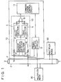
- a multiplex transmission system comprises a plurality of multiplex nodes 10, 20 and 30 and multiplex transmission lines (buses) 1 and 2.
- the multiplex nodes 10, 20 and 30 are connected individually in parallel with two common buses 1 and 2, and data signals are transmitted through the buses 1 and 2.
- Terminal circuits 3 and 7 are connected individually to the opposite ends of the buses 1 and 2.
- These multiplex nodes 10, 20 and 30 are constructed in the same manner, so that only the arrangement of the node 10 will be described below for simplicity.
- the multiplex node 10 is composed of a communication control circuit 11 for communication processing control, a transmitter circuit 12 for receiving transmitter signals from the control circuit 11 and sending them to the buses 1 and 2, a receiver circuit 13 for delivering receiver signals, fetched from the buses 1 and 2, to the circuit 11, and the like.
- the communication control circuit 11 performs communication processing control such that it fetches output signals from various apparatuses (not shown) connected thereto, frames these output signals in predetermined data units, and delivers the framed signals as the transmitter signals to the transmitter circuit 12. Like these transmitter signals, framed receiver signals are fetched from the receiver circuit 13 by the control circuit 11. Also, the communication control circuit 11 fetches only necessary signals for local use, among other receiver signals, and delivers them to the individual apparatuses connected thereto. If signals transmitted from the other multiplex nodes are normally received by the receiver circuit 13, furthermore, the control circuit 11 performs communication processing control such that it delivers a reception acknowledgment signal (hereinafter referred to as ACK signal) to the transmitter circuit 12.
- ACK signal reception acknowledgment signal
- the transmitter circuit 12 which is connected to the buses 1 and 2, transmits the transmitter signals (including the ACK signal) from the communication control circuit 11 to the buses 1 and 2 in a transmission mode for multiplex transmission.
- the circuit 12 is provided with a noise killer circuit (mentioned later) which prevents noises from being generated from the buses during the transmission.
- the receiver circuit 13 is composed of resistors 14 and 15, a passive potential detector section 16, bias sections 17 and 18, and a reception comparator 19.
- Figs. 2 and 3 are circuit diagrams illustrating second and third embodiments, respectively, of the receiver circuit, in which three signal transmission lines are used.
- the receiver circuit basically operates in the same manner as in the arrangement of Fig. 1 in which the signal transmission lines are two in number, and therefore, the particulars thereof are omitted.
- One of multiplex nodes controls a voltage setting circuit (not shown), and the potential of a bus 6 is fixed without regard to its mode, dominant or passive. If the potential of the bus 6 is a passive one, no passive potentials have to be detected.
- a passive potential detector section 21 may be omitted.
- like reference numerals are used to designate like components throughout the several views for simplicity of illustration.
- resistors 60 and 61 for differentiating the respective potentials of input lines (buses) 4 and 5 are connected to the buses 4 and 5, respectively, in these embodiments.
- the resistors 14 and 15 are connected to the reception comparator 19 by means of the buses 4 and 5, respectively, and serve as attenuators for lowering the respective potentials V1 and V2 of the buses 1 and 2 to levels such that the comparator 19 can receive signals.
- resistors 16a and 16b are connected between the buses 1 and 2, and an intermediate potential is detected as a passive-mode potential V3 of the buses 1 and 2.
- the potential V3 is delivered to the bias sections 17 and 18 in the arrangement of Fig. 1.
- the potential V3 is delivered to the bias section 17.
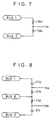
- Fig. 8 illustrates a detailed circuit arrangement of the potential detector section 21 shown in Fig. 2.
- the detector section 21 is composed of a diode 21a and a resistor 21b connected to the buses 1 and 6, respectively, and a diode 21c and a resistor 21d connected to the buses 2 and 6, respectively.
- Potentials V3a and V3b delivered from between these diodes and resistors are used as passive potentials.
- the passive potentials V3a and V3b are set so that they output the potential V6 of the bus 6 when V1 ⁇ V6 ⁇ V2 is given, that the potential V3a outputs the potential V1 of the bus 1 when V1 ⁇ V6 is given, and that the potential V3b outputs the potential V2 of the bus 2 when V6 ⁇ V2 is given.
- the input waveforms of the comparator 19 correspond to potentials within a predetermined range. At the point of change of the modes, the input waveforms of the comparator 19 cross. This situation will be described in detail later.
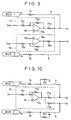
- the bias section 17 is composed of an operational amplifier 17a and resistors 17b to 17d
- the bias section 18 is composed of an operational amplifier 18a and resistors 18b to 18d.
- the bias sections 17 and 18 applies an analog bias to the buses 4 and 5, corresponding to the passive potentials V3a and V3b (potential V3 for the case of two signal transmission lines shown in Fig. 1) inputted from the passive potential detector section 21, so that potentials V4 and V5 of the buses 4 and 5 are set within a predetermined range without regard to variations of the potentials of the buses 1 and 2.
- These bias sections may reduced to one in number.
- Fig. 10 shows an embodiment for this case, in which resistors 17e, 60 and 61 are additionally used.
- the output potential of the amplifier 17a acts so that the potential of a negative input terminal of the amplifier 17a is equal to the reference potential Va.
- the potential V4 can be set within the predetermined range.
- the output potential of the amplifier 18a acts so that the potential of a negative input terminal of the amplifier 18a is equal to the reference potential Vb.
- the potential V5 can be set within the predetermined range.
- the reception comparator 19 comparing the potentials V4 and V5 inputted from the buses 4 and 5, recognizes received data signals (including the ACK signal), it delivers the signals to the communication control circuit 11.
- the reception comparator 19 can exhibit data without regard to the potentials V1 and V2 of the buses 1 and 2 if the passive mode (indicated by "P") and the dominant mode (indicated by "D") are established on the buses 1 and 2, as shown in Figs. 11(a) to 11(c) and Figs. 12(a) to 12(g).
- the respective waveforms of the received data signals get within a voltage range for reception, and are crossed at the points of change of the signals (from the passive mode to the dominant mode, and vice versa).
- the passive mode as shown in Figs.
- the respective potentials V4 and V5 of the buses 4 and 5 are set within the fixed range so that the potential V4 is lower than the potential V5. In the dominant mode, on the other hand, the potential V4 is higher than the potential V5. Thus, the potentials V4 and V5 for the passive and dominant modes cross each other.
- the receiver circuit of each multiplex node applies the bias to the buses 4 and 5 for the data signals, connected to the signal transmission lines 1 and 2, respectively, on the basis of the potentials for the passive mode, thereby setting the received potentials within the predetermined range. Even if the potentials of the buses 1 and 2 vary due to failure of the buses, therefore, the communication control circuit 11 can recognize the data signals on the buses 1 and 2 when the buses 1 and 2 become dominant.
- the bus 1 will be described first. If the signal waveforms on the bus are the ones shown in Figs. 12(a), 12(b), 12(c), 12(e) and 12(g), the potential of the bus 1 cannot change in the opposite direction (or become lower than the potential of the bus 6) in the dominant mode and in a state of which the passive-mode potentials of the buses 1 and 6 are equal. Therefore, the passive potential detector section 21 delivers the potential V6 of the bus 6 as the potential V3a (see Fig. 8) to the bias section 17. Thus, the passive-mode potential V4 of the bus 4 is set within the predetermined range.
- the passive- or dominant-mode potential of the bus 1 changes in the opposite direction (or becomes lower than the potential of the bus 6).
- the passive potential detector section 21 In order to set the passive-mode potential V4 of the bus 4 within the predetermined range, therefore, the passive potential detector section 21 must deliver the potential V1 of the bus 1 to the bias section 17. At this point of time, however, the potential V3a from the detector section 21 is higher than the potential V1 of the bus 1 by a forward potential VDa of the diode 21a.
- the passive potential detector section 21 delivers the potential V6 of the bus 6 as the potential V3b (see Fig. 8) to the bias section 18.
- the passive- or dominant-mode potential of the bus 2 changes in the opposite direction (or becomes higher than the potential of the bus 6).
- the passive potential detector section 21 delivers the potential V2 of the bus 2 to the bias section 18.
- the respective potentials V4 and V5 of the buses 4 and 5 connected to the buses 1 and 2, respectively can be set within the predetermined range even though the respective potentials V1 and V2 change in the passive mode, and the signal waveforms on the buses 4 and 5 are crossed in the dominant mode.
- the reception comparator 19 can exhibit the changes of mode of the buses 1 and 2.
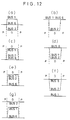
- Fig. 13 is a circuit diagram illustrating an arrangement of a seventh embodiment of the receiver circuit, in which three signal transmission lines are used.
- the passive potential which normally is the potential V6 of the bus 6 may be the potential of the bus 1 or 2 according to circumstances.
- This embodiment differs from the second embodiment in the arrangement of the section for the generation of the respective input reference potentials Va and Vb of the bias sections 17 and 18.
- this section is composed of resistors 31 to 38 and 41 to 48, comparators 39 and 49, and transistors 40 and 50.
- the potential of the bus 1 is passive, that is, if it is lower than the potential of the bus 6, according to this embodiment, for example, a potential obtained by adding the voltage drop VDa in the diode 21a is delivered from the transistor 40 to the bias section 17.
- the input reference potential Va is increased so as to cancel the voltage drop VDa.
- the input reference potential Va is determined depending on the resistors only, as in the case of the second embodiment. If the signal waveforms are the ones shown in Figs. 12(d) and 12(f), however, the comparator 39 in the circuit on the side of the bus 1 detects this state, and the transistor 40 is turned on to raise the input reference potential Va. Thus, in this embodiment, the influence of the voltage drop VDa can be removed, and the variation of the ground offset of the individual multiplex nodes can be canceled.
- the input reference potential Vb is determined depending on the resistors only. If the signal waveforms are the ones shown in Figs. 12(e) and 12(g), however, the comparator 49 in the circuit on the side of the bus 2 detects this state, and the transistor 50 is turned on to lower the input reference potential Vb.
- the potential of the bus 6 undergoes no variation attributable to the mode change, so that the passive potential is equal to the potential V6 of the bus 6. If the bus potential is opposite (or if the signal waveforms are the ones shown in Figs. 12(d) to 12(g)), however, the potential V6 of the bus 6 cannot be made passive. This is because if the bias is applied on the basis of the potential V6 of the bus 6 when the waveforms are the ones shown in Figs. 12(d) and 12(f), for example, the potential V4 of the bus 4 becomes lower than the input reference potential Va, so that the potential V4 of the bus 4 cannot exceeds the potential V5 of the bus 5 even in the dominant mode.
- a passive potential is used as the potential of the bus 1 in the circuit of Fig. 13.
- the present invention is not, however, limited to this arrangement.
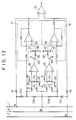
- Fig. 14 shows an example of the circuit which gives practical effect to the alternative method described above.
- this receiver circuit comprises the bias sections 17 and 18 and voltage restricting sections 51 and 52.
- the voltage restricting section 51 which includes an operational amplifier 51a, diodes 51b and 51c, and a resistor 51d, restricts the voltage lest the potential V4 of the bus 4 be lower than the input reference potential Va.
- the voltage restricting section 52 which includes an operational amplifier 52a, diodes 52b and 52c, and a resistor 52d, restricts the voltage lest the potential V5 of the bus 5 be higher than the input reference potential Vb.
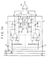
- Fig. 15 shows an embodiment for this case.
- resistors 14a and 15a which connect the output of the operational amplifier 17a of the bias section 17 and the diodes 51b and 52b, respectively, and resistors 60, 60a, 61 and 61a are additionally used.
- the resistors 17b, 14a, 18b and 15a have the same resistance value
- the resistors 60, 60a, 61 and 61a have the same resistance value
- the passive potentials Va and Vb are equal to those of the buses 4 and 5 as input lines.
- the potential of the positive input terminal of the operational amplifier 51a in the circuit on the side of the bus 1, is a potential obtained by adding the input reference potential Va and a forward voltage VDb of the diode 51b. Since the output potential of the amplifier 51a serves to make the respective potentials of its positive and negative input terminals, moreover, it is equal to (Va + VDb). If the diodes 51b and 51c are the same kind, the forward potential of the diode 51c is, therefore, equal to VDb. The diode allows no electric current to flow unless a potential difference not smaller than the value of the forward potential VDb is produced.
- the voltage restricting section 51 can prevent the potential V4 from becoming lower than the input reference potential Va. Also, the section 51 can cancel variations of the forward voltages of the diodes caused by the influence of temperature.
- the voltage restricting section 52 acts lest the potential V5 of the bus 5 be higher than the input reference potential Vb.
- the signal waveforms shown in Figs. 12(d) and 12(e) change into the waveforms on the buses 4 and 5 shown in Figs. 11(e) and 11(f), respectively, and the reception comparator 19 can exhibit the passive or dominant mode.
- the input waveforms of the comparator can be set within a predetermined potential range without regard to the variations of the potentials of the signal transmission lines, if the passive mode (state without signals) and the dominant mode (state with signals) are established on the transmission lines.
- the input waveforms are crossed at the points of change of the mode of the signal transmission lines. Accordingly, in the receiver circuit of this embodiment, the data signals can be normally received even in case of failure of the transmission lines. Since this receiver circuit, unlike the conventional one, is not designed for switching receiver signals, moreover, its configuration is simple.
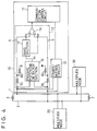
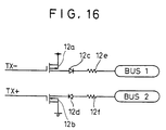
- the terminal circuits 3 and 7 are generally constructed in the manner shown in Fig. 4, while the transmitter circuit 12 is arranged as shown in Fig. 16.
- the transmitter circuit 12 shown in Fig. 16 comprises filed-effect transistors (hereinafter referred to as FETs) 12a and 12b for use as drivers, diodes 12c and 12d for protecting the FETs 12a and 12b, and resistors 12e and 12f.
- the FETs 12a and 12b are suited for high-speed data transmission.
- the buses 1 and 2 are connected with the P- and N-channel FETs 12a and 12b, respectively, and perform balanced transmission. Symbols TX+ and TX- designate the respective inputs of FET gates. If the multiplex transmission lines are two in number, the signal waveforms on the normal bus for the balanced transmission behave in the manner shown in Fig. 11(a).
- Fig. 17(a) shows a waveform which is indicative of the case that the N-channel FET 12b is turned on and off earlier. More specifically, this waveform is pulled toward the N channel, which is switched earlier, when the FET is turned on, and toward the P channel, which is switched later, when the FET is turned off.
- FIG. 17(b) shows a waveform which is indicative of the case that the P-channel FET 12a is turned on and off earlier.
- Fig. 17(c) shows a waveform which is indicative of the case that the N-channel FET 12b is turned on earlier and the P-channel FET 12a is turned off earlier.
- Fig. 17(d) shows a waveform which is indicative of the case that the P-channel FET 12a is turned on earlier and the N-channel FET 12b is turned off earlier.
- Figs. 17(e) to 17(h) show similar signal waveforms for the case of three multiplex transmission lines.
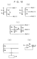
- Fig. 18 shows circuit diagrams illustrating several embodiments of the terminal circuits for waveform shaping according to the present invention. Since the terminal circuits 3 and 7 are constructed in like manner, only the circuit 3 will be described below.
- Fig. 18(a) is a circuit diagram illustrating an example of the terminal circuit 3 which uses two multiplex transmission lines.
- the terminal circuit 3 is composed of terminal resistors 3a and 3b of the same resistance value.
- Capacitors 3c1 and 3c2 are connected to the middle point between the resistors 3a and 3b.
- a switching delay can be absorbed by the capacities of the capacitors so that the signals waveforms on the buses 1 and 2 can retain their shapes even though the leading and trailing edges of the waveforms on the buses are not completely coincident.
- Fig. 18(b) is a circuit diagram illustrating another example of the terminal circuit 3 which uses three multiplex transmission lines. Referring to Fig. 18(b), the capacitors 3c1 and 3c2 are connected to the middle point between the terminal resistors 3a and 3b in the terminal circuit 3, as in the arrangement shown in Fig. 18(a).
- Fig. 18(c) is a circuit diagram illustrating still another example of the terminal circuit 3 which also uses three multiplex transmission lines.
- the terminal circuit 3 is arranged so that capacitors 3c1, 3c2, 3d1 and 3d2 and a coil 3e are connected to the bus 6.
- the capacitors 3c1, 3c2, 3d1 and 3d2 and the coil 3e can serve as filter means for restraining high-frequency noises from the bus 6.
- Fig. 18(d) is a circuit diagram illustrating a further example of the terminal circuit 3 which also uses three multiplex transmission lines.
- the terminal circuit 3 is arranged so that a power supply unit 3f and the like are connected to the bus 6.
- the potential of the bus 6 is kept within a fixed range by means of the power supply unit 3f, so that the noises from the bus 6 can be restrained.
- Fig. 18(e) shows an operational amplifier 3g as an example of the power supply unit 3f.
- the potential of the bus 6 can be kept within the fixed range.
- the amplifier 3g serves to keep its output potential at V6 in a manner such that the potential V6 of the bus 6 is fetched to its positive input, and its negative input is connected to its output.
- Figs. 19 to 22 show circuit diagrams illustrating several embodiments of the transmitter circuit according to the present invention.
- Fig. 19(a) illustrates an embodiment in which resistors 12A and 12B are connected to the gates of the FETs 12a and 12b, respectively, of the transmitter circuit shown in Fig. 16.
- the switching time for the FETs 12a and 12b can be adjusted by means of the resistors 12A and 12B.
- a delay circuit is formed by utilizing the respective input capacities of the gates of the FETs 12a and 12b and additionally using the resistors 12A and 12B.
- This embodiment can be utilized for the waveforms shown in Figs. 17(a), 17(b), 17(e) and 17(f).
- the switching speed is lowered by connecting the resistor to the FET of the higher switching speed.
- the P- and N-channel FETs are switched with the same timing, so that the signal waveforms on the buses can be shaped up.
- a CR circuit is formed by connecting the resistors 12A and 12B, so that the leading and trailing edges of the signal waveforms can be made gently-sloping.
- some switching delay can be ignored, so that the radiation of radio noises can be restrained.
- the difference between the respective ON resistances of the FETs 12a and 12b can be adjusted by means of the resistors 12e and 12f.
- Fig. 19(b) illustrates an embodiment in which a capacitor 12C is connected between the respective sources of the FETs 12a and 12b.
- the power supply is restrained from shaking at the time of on-off operation, and the signal waveforms on the buses can be can be shaped up.
- Fig. 19(c) illustrates an embodiment in which coils 12D and 12E are connected to the sources of the FETs 12a 12b, respectively.
- the on-state rush current can be restrained to make the leading edge gentle-sloping, so that the switching delay between the P and N channels can be absorbed.
- frequency-component noises at the leading edge can be removed, so that the radiation of radio noises can be restrained.
- Diodes 12F and 12G which are connected in parallel with the coils 12D and 12E, respectively, serve to prevent production of reverse starting voltages in the coils when the FETs 12a and 12b are turned off.
- Fig. 20(a) illustrates an embodiment in which an N-channel FET 12H and a resistor 12I are connected to the gate side of the P-channel FET 12a, and a P-channel FET 12J and a resistor 12K are connected to the gate side of the N-channel FET 12b.
- the switching delay between the P and N channels can be canceled.
- the P-channel FETs 12a and 12J, which are identical elements of one type, and the N-channel FETs 12b and 12H, which are identical elements of another type are combined with one another.
- the timing for the leading and trailing edges of the P and N channels which is irregular as shown in Figs. 17(c), 17(d), 17(g) and 17(h), can be regularized when the data are outputted.
- Figs. 20(b) and 20(c) illustrate embodiments in which filter means is connected to the gate side of the FETs 12a and 12b.
- the filter means of Fig. 20(b) is composed of ferrite beads 12L and 12M
- the filter means of Fig. 20(c) are composed of coils 12N and 120 and capacitors 12P1, 12Q1, 12P2, 12Q2, 12R1, 12S1, 12R2 and 12S2.
- Fig. 20(d) illustrates an embodiment in which exclusive OR circuits (hereinafter referred to as XORs) 12T and 12U are connected to the gate side of the FETs 12a and 12b.
- XORs exclusive OR circuits
- this embodiment is effective when the inputs TX+ and TX- of the FET gates cannot be synchronously switched.
- the input of the one XOR is at high level, an inverted version of the input of the other XOR is outputted.
- the input of the one XOR is at low level, on the other hand, the input state of the other XOR is outputted.
- the XORs 12T and 12U are logical elements of the same type, the respective gate input waveforms of the FETs 12a and 12b share the same timing.
- Figs. 21(a) and 21(b) illustrate embodiments in which a CR circuit is formed by connecting capacitors 12V1, 12V2, 12W1 and 12W2 between the diodes 12c and 12d and the resistors 12e and 12f or between the FETs 12a and 12b and the diodes 12c and 12d.
- the on-off operation of the FETs 12a and 12b can be blunted.
- the difference between the embodiments of Figs. 21(a) and 21(b) lies in that the capacity between the transmission lines cannot be increased in the arrangement of Fig. 21(b). Referring to Fig.
- the capacitors 12V1 and 12V2 are connected between the FET 12a and the diode 12c, while the capacitors 12W1 and 12W2 are connected between the FET 12b and the diode 12d.
- these capacitors are operative only during transmission. This is because the bus signal waveforms transmitted from other nodes during reception are prevented from reaching the capacitors 12V1, 12V2, 12W1 and 12W2 by the diodes 12c and 12d.
- Fig. 21(c) illustrates an embodiment in which capacitors 12X1, 12X2, 12Y1 and 12Y2 are connected to the gate side of the FETs 12a and 12b.
- the signal waveforms from the FET gates are blunted so that the frequency component at the leading edge is removed.
- the timing for the rise and fall of the FETs 12a and 12b can be regulated by adjusting the respective capacitance values of the capacitors 12X1, 12X2, 12Y1 and 12Y2.
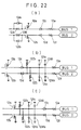
- Fig. 22(a) illustrates an embodiment in which diodes 12A1 and 12B1 are connected in parallel with the gate resistors 12A and 12B of the circuit shown in Fig. 19(a).
- the fall of each signal waveform can be made faster than that of the signal waveforms (see Fig. 24(a)) on the buses 1 and 2 shown in Fig. 19(a), so that the signal delay can be reduced, as shown in Fig. 24(b).
- the leading and trailing edges of the bus signal waveforms are switched with the same timing, more noises are produced when the current flows, that is, at the leading edges of the signal waveforms, and less at the trailing edges.
- the leading edges of the signal waveforms are made gently-sloping, and the delay of the trailing edges is reduced, so that the transmission speed can be increased.
- Figs. 22(b) and 22(c) illustrate embodiments in which resistors 12Z1 and 12Z2 are connected between the diodes 12c and 12d and the resistors 12e and 12f or between the FETs 12a and 12b and the diodes 12c and 12d of the circuit shown in Figs. 21(a) and 21(b).
- the fall of the bus signal waveforms can be quickened.
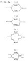
- Figs. 23(a) and 23(b) illustrate embodiments in which bias resistors 24a, 24b, 24c and 24d are connected across the terminal circuits 3 and 7 in a network including two or more multiplex transmission lines.
- bias resistors 24a, 24b, 24c and 24d are connected across the terminal circuits 3 and 7 in a network including two or more multiplex transmission lines.
- Fig. 24(c) if one of the terminal circuits is disengaged, reflected waves are produced, resulting in a delay at the trailing edge of each signal waveform, as shown in Fig. 24(c). Bias voltage is applied across the bias resistors 24a and 24d in a manner such that the resistors on the side of the bus 1 is connected to the ground and the resistors on the side of the bus 2 to Vcc. Even though the reflected waves are generated, therefore, their influence can be removed, as shown in Fig. 24(d). Thus, the receiver circuit can normally receive data signals.
- Figs. 23(c) and 23(d) illustrate embodiments in which resistors 24e, 24f and 24g are connected between and near the middle of the buses. Thus, according to these embodiments, the impedance between the buses can be lowered, and the influence of the reflected waves can be removed.
- Fig. 23(c) is a circuit diagram illustrating a two-bus arrangement
- Fig. 23(d) is a circuit diagram illustrating a three-bus arrangement.
- the terminal circuits shown in Fig. 18 and the transmitter circuits of the embodiments shown in Figs. 19 to 23 may be used in combination with one another.
- the receiver circuits of the various embodiments may be used in combination.
- transistors may be used in place of the FETs 12a and 12b according to the embodiments described herein.
- bus-type configurations have been described in connection with the embodiments shown in Fig. 23, the present invention is not limited to this type, and may be also applied to loop-type configurations.
Landscapes
- Engineering & Computer Science (AREA)
- Computer Networks & Wireless Communication (AREA)
- Signal Processing (AREA)
- Computer Security & Cryptography (AREA)
- Dc Digital Transmission (AREA)
- Small-Scale Networks (AREA)
Claims (14)
- Multiplexübertragungssystem für die Datenübertragung zwischen einer Vielzahl von Multiplexknoten (10, 20, 30), die mittels mindestens zweier Signalübertragungsleitungen miteinander verbunden sind, das folgendes umfaßt:Klemmanschlußschaltungen (3, 7), um die jeweiligen Klemmanschlußabschnitte der Signalübertragungsleitungen (1, 2) einzeln zu verbinden,wobei jeder Multiplexknoten (10, 20, 30) eine Senderschaltung (12) einschließt, um den Zustand der Daten auf der Grundlage der Potentialdifferenz zwischen den Signalübertragungsleitungen (1, 2) zu erfassen und um die Daten in Übereinstimmung mit dem erfaßten Zustand zu übertragen;wobei jeder Multiplexknoten (10, 20, 30) weiterhin ein Passivpotential-Erfassungsmittel (16, 21) einschließt, um das Potential zu erfassen, wenn sich der Zustand einer jeden Signalübertragungsleitung (1, 2) in einem passiven Modus befindet, GEKENNZEICHNET DURCHein Vorspannungsmittel (17, 18), um in Übereinstimmung mit dem Passivmodus-Potential, das von dem Passivpotential-Erfassungsmittel (16; 21) erfaßt wird, eine Vorspannung an die Eingabeleitungen (4, 5) von den jeweiligen Signalübertragungsleitungen (1, 2) analog anzulegen, um die Eingabepotentiale (V1, V2) der Signalübertragungsleitungen (1, 2) so einzustellen, daß sie in einen vorbestimmten Bereich fallen.
- Multiplexübertragungssystem nach Anspruch 1, dadurch gekennzeichnet, daß das Vorspannungsmittel (17, 18) das Eingabepotential von einer der Signalübertragungsleitungen (1, 2) so einstellt, daß es niedriger ist als die Eingabepotentiale von irgendeiner der anderen Signalübertragungsleitungen (1, 2), wenn der Zustand einer jeden Signalübertragungsleitung (1, 2) passiv ist, und so einstellt, daß es höher als die Eingabepotentiale der anderen Signalübertragungsleitungen ist, wenn der Zustand einer jeden Signalübertragungsleitung (1, 2) dominant ist.
- Multiplexübertragungssystem nach Anspruch 1 oder 2, dadurch gekennzeichnet, daß jede Klemmanschlußschaltung (3, 7) und die Senderschaltung (12) ein Begrenzungsmittel (3c1, 3c2) einschließt, um das auf den einzelnen Signalübertragungsleitungen (1, 2) von der Flankenkomponente eines bestimmten Steilpulses und der Asymmetrie der Schaltgeschwindigkeit der Senderschaltung (12) erzeugten Rauschen zu begrenzen.
- Multiplexübertragungssystem nach einem oder mehreren der Ansprüche 1-3, dadurch gekennzeichnet, daß jede Klemmanschlußschaltung (3, 7) einen Vorspannungswiderstand (24a, 24c) einschließt, der zwischen einer Leitung (1) der Signalübertragungsleitungen (1, 2) und der Erde verbunden ist, und einen Vorspannungswiderstand (24b, 24d) einschließt, der zwischen einer anderen Signalübertragungsleitung (2) und der Stromversorgung verbunden ist.
- Multiplexübertragungssystem nach einem oder mehreren der Ansprüche 1-4, dadurch gekennzeichnet, daß es weiterhin einen Widerstand (24e) umfaßt, der die Signalübertragungsleitungen (1, 2) im wesentlichen am Mittelpunkt davon verbindet und der dazu dient, die Impedanz zwischen den Signalübertragungsleitungen (1, 2) zu senken.
- Multiplexübertragungssystem nach einem oder mehreren der Ansprüche 1-5, dadurch gekennzeichnet, daß das PassivpotentialErfassungsmittel (16) ein Zwischenpotential (V3) der Signalübertragungsleitungen (1, 2) als das Passivmodus-Potential erfaßt, bei dem die Signalübertragungsleitungen (1, 2) nicht von der Senderschaltung (12) betrieben werden.
- Multiplexübertragungssysterrt nach Anspruch 6, dadurch gekennzeichnet, daß das Passivpotential-Erfassungsmittel (16) zwei Widerstände (16a, 16b) einschließt, die in Reihe zwischen zwei der Signalübertragungsleitungen (1, 2) verbunden sind, wobei ihr gemeinsamer Knoten als Ausgabepunkt für das Zwischenpotential (V3) dient.
- Multiplexübertragungssystem nach einem oder mehreren der Ansprüche 1-5, dadurch gekennzeichnet, daß das Passivpotential-Erfassungsmittel (21) ein erstes und ein zweites Zwischenpotential (V3a, V3b) der Signalübertragungsleitungen (1, 2, 6) als das Passivmodus-Potential erfaßt;wobei das Passivpotential-Erfassungsmittel (21) folgendes umfaßt:eine erste Diode (21c) und einen Widerstand (21d), die in Reihe zwischen einer ersten und einer zweiten Signalübertragungsleitung (1, 6) verbunden sind, wobei ihr gemeinsamer Knoten als Ausgabepunkt für das erste Zwischenpotential (V3a) dient; undeine zweite Diode (21a) und einen Widerstand (21b), die in Reihe zwischen der zweiten und einer dritten Signalübertragungsleitung (6, 2) verbunden sind, wobei ihr gemeinsamer Knoten als Ausgabepunkt für das zweite Zwischenpotential (V3b) dient.
- Multiplexübertragungssystem für die Datenübertragung zwischen einer Vielzahl von Multiplexknoten (10, 20, 30), die mithilfe von mindestens drei Signalübertragungsleitungen (1, 2, 6) miteinander verbunden sind, das folgendes umfaßt:Klemmanschlußächaltungen (3, 7), um die jeweiligen Klemmanschlußabschnitte der Signalübertragungsleitungen (1, 2, 6) einzeln zu verbinden,wobei jeder Multiplexknoten (10, 20, 30) eine Senderschaltung (12) einschließt, um den Zustand der Daten auf der Grundlage der Potentialdifferenz zwischen den Signalübertragungsleitungen (1, 2) zu erfassen und um die Daten in Übereinstimmung mit dem erfaßten Zustand zu übertragen;
dadurch gekennzeichnet, daß jeder Multiplexknoten (10, 20, 30) ein Vorspannungsmittel (17, 18) einschließt, um analog eine Vorspannung an die Eingabeleitungen (4, 5) von zwei (1, 2) der Signalübertragungsleitungen in Übereinstimmung mit dem Potential der anderen Signalübertragungsleitung (6) anzulegen, um die Eingabepotentiale (V1, V2) der zwei Signälübertragungsleitungen (1, 2) so einzustellen, daß sie in einen vorbestimmten Bereich fallen. - Multiplexübertragungssystem nach Anspruch 9, dadurch gekennzeichnet, daß jeder Multiplexknoten (10, 20, 30) ein Spannungsbegrenzungsmittel (51, 52) einschließt, um die Eingabepotentiale (V1, V2) innerhalb des vorbestimmten Bereichs zu begrenzen.
- Multiplexübertragungssystem nach den Ansprüchen 9 oder 10, dadurch gekennzeichnet, daß das Vorspannungsmittel (17, 18) die Eingabepotentiale aus den Signalübertragungsleitungen (1, 2, 6) auf eine analoge Weise ohne Rücksicht auf Veränderungen der jeweiligen Potentiale der Signalübertragungsleitungen (1, 2, 6) im vorbestimmten Bereich einstellt.
- Multiplexübertragungssystem nach einem oder mehreren der Ansprüche 9-11, dadurch gekennzeichnet, daß jede Klemmanschlußschaltung (3, 7) und die Senderschaltung (12) ein Begrenzungsmittel (3c1, 3c2) einschließt, um das auf den einzelnen Signalübertragungsleitungen (1, 2, 6) durch die Flankenkomponente eines bestimmten Steilpulses und die Asymmetrie der Schaltgeschwindigkeit der Senderschaltung (12) erzeugten Rauschen zu begrenzen.
- Multiplexübertragungssystem nach einem oder mehreren der Ansprüche 9-12, dadurch gekennzeichnet, daß jede Klemmanschlußschaltung (3, 7) einen Vorspannungswiderstand (24a, 24c) einschließt, der zwischen eine Leitung (1) der Signalübertragungsleitungen (1, 2, 6) und der Erde verbunden ist, und einen Vorspannungswiderstand (24b, 24d) einschließt, der zwischen eine andere Signalübertragungsleitung (2) und der Stromversorgung verbunden ist.
- Multiplexübertragungssystem nach einem oder mehreren der Ansprüche 9-13, dadurch gekennzeichnet, daß es weiterhin Widerstände (24f, 24g) einschließt, die die Signalübertragungsleitungen (1, 2, 6) im wesentlichen an ihrem Mittelpunkt verbindet und dazu dient, die Impedanz zwischen den Signalübertragungsleitungen (1, 2, 6) zu senken.
Applications Claiming Priority (9)
| Application Number | Priority Date | Filing Date | Title |
|---|---|---|---|
| JP26761991 | 1991-10-16 | ||
| JP267619/91 | 1991-10-16 | ||
| JP26761991 | 1991-10-16 | ||
| JP3195392 | 1992-02-19 | ||
| JP3195392 | 1992-02-19 | ||
| JP31953/92 | 1992-02-19 | ||
| JP04216740A JP3133499B2 (ja) | 1991-10-16 | 1992-08-14 | 多重伝送方式 |
| JP216740/92 | 1992-08-14 | ||
| JP21674092 | 1992-08-14 |
Publications (3)
| Publication Number | Publication Date |
|---|---|
| EP0537704A2 EP0537704A2 (de) | 1993-04-21 |
| EP0537704A3 EP0537704A3 (en) | 1995-02-15 |
| EP0537704B1 true EP0537704B1 (de) | 2000-07-26 |
Family
ID=27287528
Family Applications (1)
| Application Number | Title | Priority Date | Filing Date |
|---|---|---|---|
| EP92117536A Expired - Lifetime EP0537704B1 (de) | 1991-10-16 | 1992-10-14 | Multiplexübertragungssystem |
Country Status (3)
| Country | Link |
|---|---|
| EP (1) | EP0537704B1 (de) |
| CA (1) | CA2080657C (de) |
| DE (1) | DE69231289T2 (de) |
Family Cites Families (4)
| Publication number | Priority date | Publication date | Assignee | Title |
|---|---|---|---|---|
| EP0116603A4 (de) * | 1982-08-09 | 1984-11-22 | Advanced Micro Devices Inc | Gerät zum senden und empfangen digitaler signale. |
| US4792950A (en) * | 1987-06-17 | 1988-12-20 | Ford Motor Company | Multiplex wiring system |
| FR2627036B1 (fr) * | 1988-02-10 | 1990-07-27 | Peugeot | Interface de raccordement d'une partie de reception d'informations d'une station dans un systeme de transmission d'informations en differentiel, par deux fils de transmission, notamment dans un vehicule automobile |
| US4994690A (en) * | 1990-01-29 | 1991-02-19 | Motorola, Inc. | Split level bus |
-
1992
- 1992-10-14 DE DE69231289T patent/DE69231289T2/de not_active Expired - Fee Related
- 1992-10-14 EP EP92117536A patent/EP0537704B1/de not_active Expired - Lifetime
- 1992-10-15 CA CA002080657A patent/CA2080657C/en not_active Expired - Fee Related
Also Published As
| Publication number | Publication date |
|---|---|
| DE69231289D1 (de) | 2000-08-31 |
| EP0537704A2 (de) | 1993-04-21 |
| DE69231289T2 (de) | 2001-01-04 |
| CA2080657A1 (en) | 1993-04-17 |
| EP0537704A3 (en) | 1995-02-15 |
| CA2080657C (en) | 1997-05-20 |
Similar Documents
| Publication | Publication Date | Title |
|---|---|---|
| CN108353012B (zh) | 用于在经由总线系统接收数据时选择性地消隐总线振荡的装置和方法 | |
| KR102366501B1 (ko) | 버스 시스템용 가입자국 및 가입자국에 대한 전자기 적합성의 범위 내에서 간섭 저항성을 증대시키기 위한 방법 | |
| US7667939B2 (en) | Bus driver including control circuit for overvoltage protection | |
| US20060091915A1 (en) | Common mode stabilization circuit for differential bus networks | |
| US9614505B1 (en) | Differential driving circuit including asymmetry compensation circuit | |
| US20180041358A1 (en) | Communications device | |
| US6363066B1 (en) | Method and arrangement for combined data and power distribution using a communication bus | |
| KR100937344B1 (ko) | 통신 라인상의 스위칭된 신호를 위한 수신기 | |
| US9735820B2 (en) | Multi-current harmonized paths for low power local interconnect network (LIN) receiver | |
| US11368009B2 (en) | Circuit providing reverse current protection for high-side driver | |
| US5465255A (en) | Multiplex transmission system | |
| US20110158258A1 (en) | Communication signal processing apparatus and communication apparatus | |
| US20110130110A1 (en) | Receiver circuit adapted to communication apparatuses operative with different power voltage range | |
| EP0537704B1 (de) | Multiplexübertragungssystem | |
| EP2453620B1 (de) | Störungstolerante kommunikationsschaltung | |
| US12334993B2 (en) | Delay signal generation circuit, transmission circuit, electronic control unit, and vehicle | |
| US20230388161A1 (en) | Transmission circuit, electronic control unit, and vehicle | |
| JPH0964826A (ja) | データ通信装置 | |
| US7281151B2 (en) | Method of stopping data communication of a communication apparatus based on a detection of a power supply voltage drop | |
| JPH10163896A (ja) | パルス幅検出機能を有する受信スケルチ回路 | |
| US12388476B2 (en) | Transmission circuit, electronic control unit, and vehicle | |
| US7064581B2 (en) | Bus interface and method for coupling a bus device to a bus | |
| HK1066947A (en) | Receiver for a switched signal on a communication line |
Legal Events
| Date | Code | Title | Description |
|---|---|---|---|
| PUAI | Public reference made under article 153(3) epc to a published international application that has entered the european phase |
Free format text: ORIGINAL CODE: 0009012 |
|
| AK | Designated contracting states |
Kind code of ref document: A2 Designated state(s): DE FR GB IT |
|
| PUAL | Search report despatched |
Free format text: ORIGINAL CODE: 0009013 |
|
| AK | Designated contracting states |
Kind code of ref document: A3 Designated state(s): DE FR GB IT |
|
| 17P | Request for examination filed |
Effective date: 19950725 |
|
| 17Q | First examination report despatched |
Effective date: 19981113 |
|
| GRAG | Despatch of communication of intention to grant |
Free format text: ORIGINAL CODE: EPIDOS AGRA |
|
| GRAG | Despatch of communication of intention to grant |
Free format text: ORIGINAL CODE: EPIDOS AGRA |
|
| GRAH | Despatch of communication of intention to grant a patent |
Free format text: ORIGINAL CODE: EPIDOS IGRA |
|
| GRAH | Despatch of communication of intention to grant a patent |
Free format text: ORIGINAL CODE: EPIDOS IGRA |
|
| GRAA | (expected) grant |
Free format text: ORIGINAL CODE: 0009210 |
|
| AK | Designated contracting states |
Kind code of ref document: B1 Designated state(s): DE FR GB IT |
|
| PG25 | Lapsed in a contracting state [announced via postgrant information from national office to epo] |
Ref country code: IT Free format text: LAPSE BECAUSE OF FAILURE TO SUBMIT A TRANSLATION OF THE DESCRIPTION OR TO PAY THE FEE WITHIN THE PRE;WARNING: LAPSES OF ITALIAN PATENTS WITH EFFECTIVE DATE BEFORE 2007 MAY HAVE OCCURRED AT ANY TIME BEFORE 2007. THE CORRECT EFFECTIVE DATE MAY BE DIFFERENT FROM THE ONE RECORDED.SCRIBED TIME-LIMIT Effective date: 20000726 |
|
| REF | Corresponds to: |
Ref document number: 69231289 Country of ref document: DE Date of ref document: 20000831 |
|
| PG25 | Lapsed in a contracting state [announced via postgrant information from national office to epo] |
Ref country code: GB Free format text: LAPSE BECAUSE OF NON-PAYMENT OF DUE FEES Effective date: 20001026 |
|
| ET | Fr: translation filed | ||
| PLBE | No opposition filed within time limit |
Free format text: ORIGINAL CODE: 0009261 |
|
| STAA | Information on the status of an ep patent application or granted ep patent |
Free format text: STATUS: NO OPPOSITION FILED WITHIN TIME LIMIT |
|
| GBPC | Gb: european patent ceased through non-payment of renewal fee |
Effective date: 20001026 |
|
| 26N | No opposition filed | ||
| PGFP | Annual fee paid to national office [announced via postgrant information from national office to epo] |
Ref country code: FR Payment date: 20021008 Year of fee payment: 11 |
|
| PGFP | Annual fee paid to national office [announced via postgrant information from national office to epo] |
Ref country code: DE Payment date: 20021017 Year of fee payment: 11 |
|
| PG25 | Lapsed in a contracting state [announced via postgrant information from national office to epo] |
Ref country code: DE Free format text: LAPSE BECAUSE OF NON-PAYMENT OF DUE FEES Effective date: 20040501 |
|
| PG25 | Lapsed in a contracting state [announced via postgrant information from national office to epo] |
Ref country code: FR Free format text: LAPSE BECAUSE OF NON-PAYMENT OF DUE FEES Effective date: 20040630 |
|
| REG | Reference to a national code |
Ref country code: FR Ref legal event code: ST |