EP0539028A2 - ISDN-Terminierungseinheit für Wartungszwecke - Google Patents
ISDN-Terminierungseinheit für Wartungszwecke Download PDFInfo
- Publication number
- EP0539028A2 EP0539028A2 EP92308693A EP92308693A EP0539028A2 EP 0539028 A2 EP0539028 A2 EP 0539028A2 EP 92308693 A EP92308693 A EP 92308693A EP 92308693 A EP92308693 A EP 92308693A EP 0539028 A2 EP0539028 A2 EP 0539028A2
- Authority
- EP
- European Patent Office
- Prior art keywords
- coupled
- capacitor
- unit according
- signal
- customer
- Prior art date
- Legal status (The legal status is an assumption and is not a legal conclusion. Google has not performed a legal analysis and makes no representation as to the accuracy of the status listed.)
- Granted
Links
Images

Classifications
-
- H—ELECTRICITY
- H04—ELECTRIC COMMUNICATION TECHNIQUE
- H04M—TELEPHONIC COMMUNICATION
- H04M3/00—Automatic or semi-automatic exchanges
- H04M3/22—Arrangements for supervision, monitoring or testing
- H04M3/26—Arrangements for supervision, monitoring or testing with means for applying test signals or for measuring
- H04M3/28—Automatic routine testing ; Fault testing; Installation testing; Test methods, test equipment or test arrangements therefor
- H04M3/30—Automatic routine testing ; Fault testing; Installation testing; Test methods, test equipment or test arrangements therefor for subscriber's lines, for the local loop
- H04M3/301—Circuit arrangements at the subscriber's side of the line
-
- H—ELECTRICITY
- H04—ELECTRIC COMMUNICATION TECHNIQUE
- H04M—TELEPHONIC COMMUNICATION
- H04M3/00—Automatic or semi-automatic exchanges
- H04M3/22—Arrangements for supervision, monitoring or testing
- H04M3/24—Arrangements for supervision, monitoring or testing with provision for checking the normal operation
- H04M3/244—Arrangements for supervision, monitoring or testing with provision for checking the normal operation for multiplex systems
- H04M3/245—Arrangements for supervision, monitoring or testing with provision for checking the normal operation for multiplex systems for ISDN systems
-
- H—ELECTRICITY
- H04—ELECTRIC COMMUNICATION TECHNIQUE
- H04Q—SELECTING
- H04Q11/00—Selecting arrangements for multiplex systems
- H04Q11/04—Selecting arrangements for multiplex systems for time-division multiplexing
- H04Q11/0428—Integrated services digital network, i.e. systems for transmission of different types of digitised signals, e.g. speech, data, telecentral, television signals
- H04Q11/0435—Details
- H04Q11/045—Selection or connection testing arrangements
-
- H—ELECTRICITY
- H04—ELECTRIC COMMUNICATION TECHNIQUE
- H04Q—SELECTING
- H04Q2213/00—Indexing scheme relating to selecting arrangements in general and for multiplex systems
- H04Q2213/1318—Ringing
-
- H—ELECTRICITY
- H04—ELECTRIC COMMUNICATION TECHNIQUE
- H04Q—SELECTING
- H04Q2213/00—Indexing scheme relating to selecting arrangements in general and for multiplex systems
- H04Q2213/13202—Network termination [NT]
-
- H—ELECTRICITY
- H04—ELECTRIC COMMUNICATION TECHNIQUE
- H04Q—SELECTING
- H04Q2213/00—Indexing scheme relating to selecting arrangements in general and for multiplex systems
- H04Q2213/13209—ISDN
-
- H—ELECTRICITY
- H04—ELECTRIC COMMUNICATION TECHNIQUE
- H04Q—SELECTING
- H04Q2213/00—Indexing scheme relating to selecting arrangements in general and for multiplex systems
- H04Q2213/13302—Magnetic elements
-
- H—ELECTRICITY
- H04—ELECTRIC COMMUNICATION TECHNIQUE
- H04Q—SELECTING
- H04Q2213/00—Indexing scheme relating to selecting arrangements in general and for multiplex systems
- H04Q2213/13305—Transistors, semiconductors in general
-
- H—ELECTRICITY
- H04—ELECTRIC COMMUNICATION TECHNIQUE
- H04Q—SELECTING
- H04Q2213/00—Indexing scheme relating to selecting arrangements in general and for multiplex systems
- H04Q2213/1332—Logic circuits
Definitions
- This invention relates to Maintenance Termination Units (MTUs).
- POTS MTUs generally rely on the presence of a DC current on the line to close a solid state switch when the customer is off-hook.
- ISDN Integrated Services Digital Network
- the invention is a maintenance termination unit comprising means responsive to a ringing signal for generating an AC signal, means for rectifying the signal, and a capacitor coupled to the rectifier means.
- the unit further comprises a normally closed semiconductor switch.
- the capacitor is coupled to the switch such that when the capacitor is charged, the switch will open.
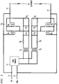
- a maintenance termination unit in accordance with one embodiment is illustrated in FIG. 1.
- Data, voice, or video signals are supplied from the central office to input tip and ring conductors 11 and 12.
- the incoming signals are supplied to a tone ringer circuit 13.
- the tone ringer circuit is a commercially available circuit designed to produce an AC signal (tone) in response to a ringing signal on the lines 11 and 12.
- One such circuit which is generally used to create AC tones on speakerphones, is made by Motorola under the designation MC 34017-2P.
- the AC signal will have a frequency in the range 100-1000 Hz and a peak amplitude in the range 1-5 volts.
- the output of the tone ringer is coupled to a transformer, T1, which is used to isolate the remainder of the unit from voltages on the tip and ring conductors.
- the transformer, T1 has a turn ratio of 1:1.
- the output of the transformer is coupled to a rectifying means which, in this example, is a standard silicon rectifying diode D1.
- a capacitor, C1 has one plate coupled to conductor 14 extending from the cathode of the diode D1 and its other plate coupled to conductor 15 extending from the secondary winding of the transformer T1.
- the capacitance of C1 should be within the range 2-10 microfarads.
- a resistor R1 Coupled in parallel with the capacitor C1 is a resistor R1 which, for reasons to be discussed, has a resistance in the range 10-30 megohms.
- a zener diode D2 is also coupled in parallel with capacitor C1 and resistor R1.
- a pair of MOS Field Effect Transistors (MOSFETs), Q1 and Q2, have a common gate electrode G coupled to conductor 15 and a common source region coupled to conductor 14.
- the drain region of transistor Q1 is coupled to the tip conductor 11, and the drain of transistor Q2 is coupled to the output tip conductor 16 which is connected to the customer equipment.
- the transistors Q1 and Q2 are normally conducting, depletion mode MOSFETs.
- a capacitor C2 is coupled across the two transistors Q1 and Q2 to minimize losses of high frequency signals through the circuit during normal transmission by providing a path which bypasses Q1 and Q2 for such signals.
- C2 generally has a value in the range 0.1 to 1 microfarads.
- transistors Q1 and Q2 will be conducting so that the circuit of FIG. 1 is transparent to the central office and customer. If, however, a service problem should develop, or if the central office merely wants to conduct a routine test, a ringing signal is transmitted from the central office and appears on conductors 11 and 12. This signal, which normally has a frequency of approximately 20 Hz and an RMS amplitude of approximately 84 RMS, is not used in the normal operation of ISDN systems.
- the tone ringer, 13 detects the presence of the ringing signal and, in response, produces an AC signal at its output. This signal is applied to transformer T1 and to diode D1 for rectification.
- the rectified signal is used to quickly charge up capacitor C1.
- a certain level in this example approximately 2 volts, the depletion mode MOSFETs Q1 and Q2 will be rendered non-conductive as a result of the corresponding voltage established between the gate G and source regions of the MOSFETs.
- the customer is thereby cut off from the network while standard tests can be performed to determine if any problem exists in the network.
- MOSFETs will remain non-conducting for a period of time depending on the value of R1 since the capacitor C1 will be discharging through R1 during this disconnect interval. It is generally desirable to keep the customer disconnected for a period of 30-180 seconds. Consequently, a resistance of R1 in the range 6-30 megohms is appropriate. Once the capacitor C1 has discharged below a certain level, MOSFETs Q1 and Q2 will resume their normal conducting state, and further tests can then be performed on the customer equipment.
- the diode D2 serves as a protector element. In the event that too much voltage is generated across conductors 14 and 15, D2 will break over and conduct current away from the capacitor.
- FIG. 2 illustrates an alternative embodiment where elements corresponding to those of FIG. 1 are similarly numbered.
- a second pair of MOSFETs, Q3 and Q4 are coupled to the output ring conductor 17 to provide an additional switch.
- the additional switch is operated by a similar combination of transformer T2 coupled to the tone ringer, 13, a rectifying diode D3, capacitors C3 and C4, a resistor R2 and a zener diode D4.
- This circuit permits both central office tip and ring conductors 11 and 12 to be disconnected from the customer.
- the circuit will also add additional impedance to the lines, which can be minimized by the presence of capacitors C2 and C4 to bypass transistors Q1 - Q4 for high frequency signals.
- a single 3-winding transformer can replace the two transformers T1 and T2.
- a MOSFET with one input and two outputs, each coupled to one of the output tip and ring conductors, could simplify the circuitry of FIG.2 by eliminating T2 , D3 , C2, R2 and D4.
- a bridge circuit including tip, ring, and ground conductors can be used to provide the incoming signal to the tone ringer 13. This modification would ensure that the MTU would operate even if there is a short between tip and ring by applying the signal between tip or ring and ground.
Landscapes
- Engineering & Computer Science (AREA)
- Signal Processing (AREA)
- Computer Networks & Wireless Communication (AREA)
- Devices For Supply Of Signal Current (AREA)
- Interface Circuits In Exchanges (AREA)
- Monitoring And Testing Of Exchanges (AREA)
- Telephonic Communication Services (AREA)
Applications Claiming Priority (2)
| Application Number | Priority Date | Filing Date | Title |
|---|---|---|---|
| US77166491A | 1991-10-04 | 1991-10-04 | |
| US771664 | 1991-10-04 |
Publications (3)
| Publication Number | Publication Date |
|---|---|
| EP0539028A2 true EP0539028A2 (de) | 1993-04-28 |
| EP0539028A3 EP0539028A3 (en) | 1993-07-07 |
| EP0539028B1 EP0539028B1 (de) | 1998-08-05 |
Family
ID=25092566
Family Applications (1)
| Application Number | Title | Priority Date | Filing Date |
|---|---|---|---|
| EP19920308693 Expired - Lifetime EP0539028B1 (de) | 1991-10-04 | 1992-09-24 | ISDN-Terminierungseinheit für Wartungszwecke |
Country Status (7)
| Country | Link |
|---|---|
| EP (1) | EP0539028B1 (de) |
| JP (1) | JP2665117B2 (de) |
| AU (1) | AU634440B1 (de) |
| CA (1) | CA2077992C (de) |
| DE (1) | DE69226490T2 (de) |
| SG (1) | SG43842A1 (de) |
| TW (1) | TW263637B (de) |
Cited By (2)
| Publication number | Priority date | Publication date | Assignee | Title |
|---|---|---|---|---|
| GB2361832A (en) * | 2000-04-29 | 2001-10-31 | Marconi Comm Ltd | Telecommunications equipment |
| EP1154670A1 (de) * | 2000-05-12 | 2001-11-14 | Siemens Schweiz AG | Netzabschlussgerät für ein Teilnehmerendgerät eines Telekommunikationsnetzes und Verfahren zur Bereitstellung einer Rufleerlaufspannung für ein Teilnehmerendgerät eines Telekommunikationsnetzes |
Family Cites Families (10)
| Publication number | Priority date | Publication date | Assignee | Title |
|---|---|---|---|---|
| JPS5827708B2 (ja) * | 1979-08-06 | 1983-06-10 | 日本電信電話株式会社 | 切分試験回路 |
| JPS5931121B2 (ja) * | 1980-08-12 | 1984-07-31 | 株式会社ケンウッド | タ−ンテ−ブル装置 |
| US4374307A (en) * | 1980-08-29 | 1983-02-15 | Tandy Corporation | Ringer system for a telephone |
| GB2086186B (en) * | 1980-10-07 | 1984-06-06 | Standard Telephones Cables Ltd | Telephone answering machine intefrace |
| US4396809A (en) * | 1981-08-03 | 1983-08-02 | Bell Telephone Laboratories, Incorporated | Maintenance termination unit |
| DE3375269D1 (en) * | 1982-04-05 | 1988-02-11 | Gen Electric Co Plc | Telecommunication system loop-back unit |
| JPH0233221B2 (ja) * | 1982-09-06 | 1990-07-26 | Kawaguchi Electric Works | Kaisenbunriki |
| DE3340396C2 (de) * | 1983-11-09 | 1987-05-07 | Hagenuk GmbH, 2300 Kiel | Schaltungsanordnung für einen Rufsignalgenerator |
| DE3843785A1 (de) * | 1988-12-24 | 1990-07-12 | Standard Elektrik Lorenz Ag | Zugangseinrichtung fuer eine isdn-anschalteeinrichtung eines oeffentlichen endgeraets |
| JP2626911B2 (ja) * | 1988-12-27 | 1997-07-02 | 日本電信電話株式会社 | 遠隔切分け装置 |
-
1992
- 1992-09-01 TW TW81106919A patent/TW263637B/zh active
- 1992-09-10 CA CA 2077992 patent/CA2077992C/en not_active Expired - Fee Related
- 1992-09-16 AU AU24563/92A patent/AU634440B1/en not_active Ceased
- 1992-09-24 EP EP19920308693 patent/EP0539028B1/de not_active Expired - Lifetime
- 1992-09-24 SG SG1996002044A patent/SG43842A1/en unknown
- 1992-09-24 DE DE1992626490 patent/DE69226490T2/de not_active Expired - Fee Related
- 1992-10-02 JP JP4287020A patent/JP2665117B2/ja not_active Expired - Fee Related
Cited By (3)
| Publication number | Priority date | Publication date | Assignee | Title |
|---|---|---|---|---|
| GB2361832A (en) * | 2000-04-29 | 2001-10-31 | Marconi Comm Ltd | Telecommunications equipment |
| GB2361832B (en) * | 2000-04-29 | 2002-03-20 | Marconi Comm Ltd | Telecommunications equipment |
| EP1154670A1 (de) * | 2000-05-12 | 2001-11-14 | Siemens Schweiz AG | Netzabschlussgerät für ein Teilnehmerendgerät eines Telekommunikationsnetzes und Verfahren zur Bereitstellung einer Rufleerlaufspannung für ein Teilnehmerendgerät eines Telekommunikationsnetzes |
Also Published As
| Publication number | Publication date |
|---|---|
| SG43842A1 (en) | 1997-11-14 |
| DE69226490T2 (de) | 1999-01-07 |
| JPH06291838A (ja) | 1994-10-18 |
| CA2077992C (en) | 1998-04-21 |
| EP0539028A3 (en) | 1993-07-07 |
| AU634440B1 (en) | 1993-02-18 |
| EP0539028B1 (de) | 1998-08-05 |
| TW263637B (de) | 1995-11-21 |
| CA2077992A1 (en) | 1993-04-05 |
| JP2665117B2 (ja) | 1997-10-22 |
| DE69226490D1 (de) | 1998-09-10 |
Similar Documents
| Publication | Publication Date | Title |
|---|---|---|
| US4710949A (en) | Telephone line fault locating device | |
| US4653084A (en) | Remote actuated switch | |
| EP1005209A2 (de) | Signalisierungsverfahren zum Aufrufen eines Testmoduses in einem Netzwerkschnittstellengerät | |
| US6212258B1 (en) | Device for remotely testing a twisted pair transmission line | |
| US5020100A (en) | Telephone line loop current regulator | |
| US6618482B2 (en) | System and method for protecting devices connected to a telephone line | |
| US5198957A (en) | Transient protection circuit using common drain field effect transistors | |
| US5600715A (en) | Integrated loop current detector apparatus for a PSTN modem | |
| US5768341A (en) | Communications channel testing arrangement | |
| EP0345679A2 (de) | Fehlerschutzschaltung für Stromversorgung | |
| USRE28283E (en) | Threshold circuit for tone-ringer or like load means | |
| US5392327A (en) | Termination unit with maintenance facility | |
| EP0539028B1 (de) | ISDN-Terminierungseinheit für Wartungszwecke | |
| US6047063A (en) | Methods and apparatus for providing an auxiliary communication line | |
| US4894860A (en) | Trunk interface circuitry for telephone systems | |
| US4079205A (en) | Automatic number identification device | |
| US4369337A (en) | Central office interface circuit | |
| US5329584A (en) | Interface circuit to quickly establish a loop current | |
| US5818926A (en) | Switching device for telecommunications channel | |
| US4191859A (en) | Loop, dial pulse and ring trip detection circuit with capacitive shunt network | |
| US4204094A (en) | Tone applying line circuit | |
| US4380688A (en) | Telephone ringing range extender | |
| US5253290A (en) | Circuit arrangement for the transmission of telecommunication signals | |
| JPS5880957A (ja) | 通信装置におけるル−プ電流基準値の検出方法 | |
| US6944286B1 (en) | Ground key detection circuit and method for interference-resistant detection of the activation of a ground key for telephones |
Legal Events
| Date | Code | Title | Description |
|---|---|---|---|
| PUAI | Public reference made under article 153(3) epc to a published international application that has entered the european phase |
Free format text: ORIGINAL CODE: 0009012 |
|
| AK | Designated contracting states |
Kind code of ref document: A2 Designated state(s): DE FR GB IT |
|
| PUAL | Search report despatched |
Free format text: ORIGINAL CODE: 0009013 |
|
| AK | Designated contracting states |
Kind code of ref document: A3 Designated state(s): DE FR GB IT |
|
| 17P | Request for examination filed |
Effective date: 19931208 |
|
| RAP3 | Party data changed (applicant data changed or rights of an application transferred) |
Owner name: AT&T CORP. |
|
| 17Q | First examination report despatched |
Effective date: 19961120 |
|
| GRAG | Despatch of communication of intention to grant |
Free format text: ORIGINAL CODE: EPIDOS AGRA |
|
| GRAG | Despatch of communication of intention to grant |
Free format text: ORIGINAL CODE: EPIDOS AGRA |
|
| GRAH | Despatch of communication of intention to grant a patent |
Free format text: ORIGINAL CODE: EPIDOS IGRA |
|
| GRAH | Despatch of communication of intention to grant a patent |
Free format text: ORIGINAL CODE: EPIDOS IGRA |
|
| GRAA | (expected) grant |
Free format text: ORIGINAL CODE: 0009210 |
|
| AK | Designated contracting states |
Kind code of ref document: B1 Designated state(s): DE FR GB IT |
|
| ITF | It: translation for a ep patent filed | ||
| REF | Corresponds to: |
Ref document number: 69226490 Country of ref document: DE Date of ref document: 19980910 |
|
| ET | Fr: translation filed | ||
| PLBE | No opposition filed within time limit |
Free format text: ORIGINAL CODE: 0009261 |
|
| 26N | No opposition filed | ||
| PGFP | Annual fee paid to national office [announced via postgrant information from national office to epo] |
Ref country code: DE Payment date: 20000929 Year of fee payment: 9 |
|
| REG | Reference to a national code |
Ref country code: GB Ref legal event code: IF02 |
|
| PG25 | Lapsed in a contracting state [announced via postgrant information from national office to epo] |
Ref country code: DE Free format text: LAPSE BECAUSE OF NON-PAYMENT OF DUE FEES Effective date: 20020501 |
|
| PGFP | Annual fee paid to national office [announced via postgrant information from national office to epo] |
Ref country code: IT Payment date: 20080926 Year of fee payment: 17 Ref country code: FR Payment date: 20080915 Year of fee payment: 17 |
|
| PGFP | Annual fee paid to national office [announced via postgrant information from national office to epo] |
Ref country code: GB Payment date: 20080924 Year of fee payment: 17 |
|
| GBPC | Gb: european patent ceased through non-payment of renewal fee |
Effective date: 20090924 |
|
| REG | Reference to a national code |
Ref country code: FR Ref legal event code: ST Effective date: 20100531 |
|
| PG25 | Lapsed in a contracting state [announced via postgrant information from national office to epo] |
Ref country code: FR Free format text: LAPSE BECAUSE OF NON-PAYMENT OF DUE FEES Effective date: 20090930 |
|
| PG25 | Lapsed in a contracting state [announced via postgrant information from national office to epo] |
Ref country code: GB Free format text: LAPSE BECAUSE OF NON-PAYMENT OF DUE FEES Effective date: 20090924 |
|
| PG25 | Lapsed in a contracting state [announced via postgrant information from national office to epo] |
Ref country code: IT Free format text: LAPSE BECAUSE OF NON-PAYMENT OF DUE FEES Effective date: 20090924 |