EP0540158A2 - Apparat zur Erzeugung eines sinusförmigen Ausgangssignales - Google Patents
Apparat zur Erzeugung eines sinusförmigen Ausgangssignales Download PDFInfo
- Publication number
- EP0540158A2 EP0540158A2 EP92308329A EP92308329A EP0540158A2 EP 0540158 A2 EP0540158 A2 EP 0540158A2 EP 92308329 A EP92308329 A EP 92308329A EP 92308329 A EP92308329 A EP 92308329A EP 0540158 A2 EP0540158 A2 EP 0540158A2
- Authority
- EP
- European Patent Office
- Prior art keywords
- signal
- generating
- output
- multiplier
- frequency
- Prior art date
- Legal status (The legal status is an assumption and is not a legal conclusion. Google has not performed a legal analysis and makes no representation as to the accuracy of the status listed.)
- Granted
Links
Images

Classifications
-
- H—ELECTRICITY
- H04—ELECTRIC COMMUNICATION TECHNIQUE
- H04L—TRANSMISSION OF DIGITAL INFORMATION, e.g. TELEGRAPHIC COMMUNICATION
- H04L27/00—Modulated-carrier systems
- H04L27/10—Frequency-modulated carrier systems, i.e. using frequency-shift keying
- H04L27/12—Modulator circuits; Transmitter circuits
-
- H—ELECTRICITY
- H03—ELECTRONIC CIRCUITRY
- H03B—GENERATION OF OSCILLATIONS, DIRECTLY OR BY FREQUENCY-CHANGING, BY CIRCUITS EMPLOYING ACTIVE ELEMENTS WHICH OPERATE IN A NON-SWITCHING MANNER; GENERATION OF NOISE BY SUCH CIRCUITS
- H03B5/00—Generation of oscillations using amplifier with regenerative feedback from output to input
- H03B5/20—Generation of oscillations using amplifier with regenerative feedback from output to input with frequency-determining element comprising resistance and either capacitance or inductance, e.g. phase-shift oscillator
Definitions
- the present invention relates to an apparatus for generating a sinusoidal output signal.
- FSK frequency shift keying
- MSK minimum shift keying
- GMSK Gaussian minimum shift keying
- FSK signals are sometimes effected by circuitry involving analog devices, and such analog devices are generally bulkier and less stable (especially in temperature-varying environments) than digital devices.
- sudden frequency shifts in response to changes in signal levels of input signals generally involve undesirable noise during frequency transitions.
- the invention provides an apparatus for generating an output signal in response to an input signal having a variable input level.
- the output signal has an output frequency which varies to represent variations in the input level.
- the apparatus comprises a processing circuit for implementing a digital signal processing algorithm to generate a plurality of control signals in response to the input signal, which plurality of control signals is representative of the variable input level, and an oscillator circuit for generating the output signal in response to the plurality of control signals.
- the plurality of control signals includes a first control signal representing a first output frequency of the output signal, a second control signal representing a second output frequency of the output signal, and at least one intermediate control signal representing output frequencies of the output signal intermediate the first output frequency and the second output frequency.
- each respective intermediate control signal is associated with a respective intermediate frequency.
- the processing circuit Preferably the processing circuit generates at least one of the intermediate control signals whenever the output signal varies from the first output frequency to the second output frequency or whenever the output signal varies from the second output frequency to the first output frequency.
- Such intermediate frequency generation on every occasion of frequency shift by the oscillator circuit serves to "soften” the transition between the first and second output frequencies and reduces noise which usually is generated by such sudden changes in output frequency.
- the oscillator circuit comprises a first delay circuit which receives a first signal and generates a second signal, which second signal is delayed one clock period with respect to the first signal; and a second delay circuit which receives the second signal from the first delay circuit and generates a third signal, which third signal is delayed one clock period with respect to the second signal.
- a multiplying circuit for multiplying a signal by a multiplier. The multiplying circuit receives the second signal from the first delay circuit, receives a multiplier at a multiplier input, and generates a multiplier output signal which comprises the second signal multiplied by the multiplier.
- the oscillator circuit may include a differential circuit which receives the third signal from the second delay circuit and receives the multiplier output signal from the multiplying circuit, and generates a sinusoidal output which is the difference between the multiplier output signal less the third signal; the sinusoidal output signal is also provided in a feedback loop to the first delay circuit and is received by the first delay circuit as the first signal so that the oscillator circuit operates as a recursive oscillator.
- the multiplier received by the multiplier circuit comprises a constant which is representative of the varying input level of the input signal.
- the multiplier thus is employed as a control signal and may be generated by a control signal generator.
- a control signal generator may, in its preferred embodiment, include a scaling circuit for receiving the input signal and scaling the input signal according to at least one scaling factor to produce the control signal (i.e., the multiplier).
- a control signal generator may comprise a logic circuit receiving the input signal and an array of digital filters. The logic circuit selects one digital filter of the array of digital filters in response to the input signal level.
- the selected digital filter receives the input signal from the logic circuit and filters the input signal to produce a selected control signal appropriate to cause the oscillator circuit to generate its sinusoidal output at the correct frequency to represent the respective input signal level at hand.
- Digital filters are provided for producing appropriate control signals to yield intermediate output frequencies to reduce noise during output signal frequency excursions.
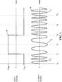
- Fig. 1 illustrates the relationship between an output signal and an input signal in a preferred embodiment of the present invention.
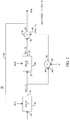
- Fig. 2 illustrates the preferred embodiment of an oscillator circuit employed in the present invention.
- Fig. 3 illustrates the preferred embodiment of the present invention.
- Fig. 4 illustrates an alternate embodiment of the present invention.
- FIG. 1 A typical frequency modulation scheme encountered in digital communications, and commonly encountered in frequency shift keyed (FSK) communication systems, is illustrated in Fig. 1.
- a digital input signal is illustrated varying over time between -V ref and +V ref so that input signal 10 is at a level -V ref from time t0 to time t1; shifts to a level +V ref at time t1, maintaining the level +V ref until time t3; and shifts to level -V ref at time t3, maintaining level -V ref from time t3 through time t5.
- Output signal 12 is modulated according to the level of input signal 10.
- output signal 12 has a frequency f1 between time t0 and time t1 when input signal 10 is at value -V ref ;
- output signal 12 has a frequency f2 during the interval between time t1 and time t3 when input signal 10 has value +V ref ;
- output signal 12 is transmitted at frequency f1 during the time interval t3 through t5 when input signal 10 again has value -V ref .
- the frequency of output signal 12 represents the signal level of input signal 10.
- a frequency function may be defined as: where f s is a sampling rate and f is a desired frequency.
- the current output x(n) is recursively related to outputs one time interval later (x(n-1)) and two time intervals later (x(n-2)), and the recursive nature of output signal x(n) can be used to generate sine waves using a sampling frequency f s that has no specific relationship to the desired frequency (f) to be generated, except that the sampling frequency must satisfy Nyquist's sampling theorem (i.e., f s ⁇ 2f).
- This recursive relationship facilitates simplified sinusoidal output signal generation. Distinct advantages are especially provided in the implementation of such recursive signal generation since prior art apparatuses employing look-up tables (read-only memories; ROM) to store wave-form samples, with the number of samples required to be stored being dependent upon the relationship between the desired frequency and the sampling rate.
- the recursive capability of the present invention requires only two storage locations, regardless of what frequency is desired. Specifically, the recursive capability of the present invention facilitates generation of a sinusoidal output signal using two successive signal samples [x(n-1), and x(n-2)]. Thus, two storage locations are all that are required for employing the recursive relationship: one storage location for x(n-1) and one storage location for x(n-2).
- Fig. 2 is an illustration of the preferred embodiment of a recursive oscillating circuit apparatus employing the above-described relationships to advantage.
- a first delay circuit 16 receives a first signal at an input 18 and generates a once-delayed output signal at an output 20.
- the once-delayed output signal is delayed one time period from the first signal received at input 18.
- the once-delayed output signal from output 20 of first delay circuit 16 is received as an input signal by a second delay circuit 24 at an input 22.
- Second delay circuit 24 produces a twice-delayed output signal at its output 26, which twice-delayed output signal is delayed one clock period from the once-delayed output signal received at its input 22.
- the once-delayed output signal from first delay circuit 16 is also provided as an input to a multiplier circuit 28 at an input 30.
- Multiplier circuit 28 multiplies the once-delayed output signal received from first delay circuit 16 by a multiplier ⁇ received at a multiplier input 32, and provides a multiplier output signal at its output 34.
- the multiplier output signal is provided to a positive node 36 of a summing unit 38.
- Summing unit 38 also receives at its negative node 40 the twice-delayed output signal from output 26 of second delay circuit 24.
- summing unit 38 provides at its output 42 a difference signal representing the difference between the multiplier output signal received at its input node 36, less the twice-delayed output signal received at its negative node 40. This difference signal is the sinusoidal output signal x(n).
- Sinusoidal output signal x(n) is provided through a feedback line 44 to first delay circuit 16 and comprises the first signal received by first delay circuit 16 at its input 18.
- a recursive oscillator circuit 15 which provides an output x(n) determined by a multiplier ⁇ received at multiplier input 32.
- Initial conditions are established for oscillator circuit 15 by an input x(1) to first delay circuit 16 and by an input x(0) to second delay circuit 24.
- recursive oscillator circuit 15 as illustrated in Fig. 2 in a communications system is illustrated, in its preferred embodiment, in Fig. 3.
- a communications system 50 is illustrated receiving a digital signal input at an input 52 to a low pass filter (or signal synthesizer) 54.
- Low pass filter 54 employs a sampling frequency f s received at an input 56.
- a signal "y" is generated from low pass filter 54 at an output 58 and passed to a scaling circuit 60.
- Scaling circuit 60 comprises a multiplier unit 62 and an adder unit 64 to which output signal "y" is successively applied.
- the scaled output ⁇ is applied to recursive oscillator 15 and recursive oscillator 15 generates an output signal at line 70 in a manner as described in connection with Fig. 2.
- the output signal at line 70 is a sinusoidal output signal which is defined by control signal ⁇ which is received by recursive oscillator 15 via line 66 from scaling circuit 60.
- a communications system 80 is illustrated comprising a logic circuit 82 which receives a digital input signal at an input 84. Depending upon the signal level of the input signal received at input 84, logic circuit 82 selects an appropriate filter among an array of filters FT1, FT2, ..., FTn for receiving a representation of the input signal on line 86.
- the selected appropriate filter for example filter FT1 in Fig. 4, filters the representative input signal received on line 86 to produce a control signal ⁇ on a line 88 for provision to a recursive oscillator 15.
- Selection of the appropriate filter FT1, FT2, ..., FTn by logic circuit 82 is preprogrammed in logic circuit 82 for effecting generation of a control signal ⁇ to facilitate effecting noise-free transition of the frequency of an output signal produced at output 90 to accurately reflect deviations in the signal level of the input signal received at input 84 of logic circuit 82.
Landscapes
- Engineering & Computer Science (AREA)
- Computer Networks & Wireless Communication (AREA)
- Signal Processing (AREA)
- Digital Transmission Methods That Use Modulated Carrier Waves (AREA)
- Manipulation Of Pulses (AREA)
- Inductance-Capacitance Distribution Constants And Capacitance-Resistance Oscillators (AREA)
- Control Of Motors That Do Not Use Commutators (AREA)
Applications Claiming Priority (2)
| Application Number | Priority Date | Filing Date | Title |
|---|---|---|---|
| US07/785,497 US5189381A (en) | 1991-10-31 | 1991-10-31 | Apparatus for generating a sinusoidal output signal |
| US785497 | 1991-10-31 |
Publications (3)
| Publication Number | Publication Date |
|---|---|
| EP0540158A2 true EP0540158A2 (de) | 1993-05-05 |
| EP0540158A3 EP0540158A3 (de) | 1994-01-12 |
| EP0540158B1 EP0540158B1 (de) | 1998-03-04 |
Family
ID=25135701
Family Applications (1)
| Application Number | Title | Priority Date | Filing Date |
|---|---|---|---|
| EP92308329A Expired - Lifetime EP0540158B1 (de) | 1991-10-31 | 1992-09-14 | Apparat zur Erzeugung eines sinusförmigen Ausgangssignales |
Country Status (6)
| Country | Link |
|---|---|
| US (1) | US5189381A (de) |
| EP (1) | EP0540158B1 (de) |
| JP (1) | JP3388596B2 (de) |
| AT (1) | ATE163816T1 (de) |
| DE (1) | DE69224584D1 (de) |
| ES (1) | ES2113925T3 (de) |
Families Citing this family (4)
| Publication number | Priority date | Publication date | Assignee | Title |
|---|---|---|---|---|
| US5339251A (en) * | 1991-11-22 | 1994-08-16 | Advanced Micro Devices, Inc. | Apparatus for adaptively tuning to a received periodic signal |
| US5343414A (en) * | 1991-11-22 | 1994-08-30 | Advanced Micro Devices, Inc. | Apparatus for adaptively tuning to a received periodic signal |
| US9772972B2 (en) | 2014-07-17 | 2017-09-26 | Syntropy Systems, Llc | Generation of high-rate sinusoidal sequences |
| US9837989B2 (en) | 2014-07-17 | 2017-12-05 | Syntropy Systems, Llc | Generation of high-rate sinusoidal sequences |
Family Cites Families (8)
| Publication number | Priority date | Publication date | Assignee | Title |
|---|---|---|---|---|
| US4555792A (en) * | 1981-10-02 | 1985-11-26 | U.S. Philips Corporation | Transmitter for transmitting an FSK-modulated signal |
| US4494073A (en) * | 1982-09-27 | 1985-01-15 | Cubic Corporation | Frequency generator using composite digitally controlled oscillators |
| FR2551279B1 (fr) * | 1983-08-24 | 1988-10-14 | Texas Instruments France | Generateur d'onde sinusoidale, dont la frequence est asservie a un signal binaire, notamment pour modem |
| US4573025A (en) * | 1984-04-02 | 1986-02-25 | Motorola, Inc. | Drift-equalized, multi-frequency oscillator |
| JPS6257303A (ja) * | 1985-09-06 | 1987-03-13 | Hitachi Ltd | デイジタル発振回路 |
| US4686489A (en) * | 1986-06-16 | 1987-08-11 | Tektronix, Inc. | Triggered voltage controlled oscillator using fast recovery gate |
| JPS6473808A (en) * | 1987-09-14 | 1989-03-20 | Oki Electric Ind Co Ltd | Sine wave oscillator |
| US5105444A (en) * | 1989-09-13 | 1992-04-14 | Atlantic Richfield Company | System for high speed data tranmission |
-
1991
- 1991-10-31 US US07/785,497 patent/US5189381A/en not_active Expired - Lifetime
-
1992
- 1992-09-14 DE DE69224584T patent/DE69224584D1/de not_active Expired - Lifetime
- 1992-09-14 AT AT92308329T patent/ATE163816T1/de not_active IP Right Cessation
- 1992-09-14 ES ES92308329T patent/ES2113925T3/es not_active Expired - Lifetime
- 1992-09-14 EP EP92308329A patent/EP0540158B1/de not_active Expired - Lifetime
- 1992-10-22 JP JP28410892A patent/JP3388596B2/ja not_active Expired - Lifetime
Also Published As
| Publication number | Publication date |
|---|---|
| JPH06112980A (ja) | 1994-04-22 |
| DE69224584D1 (de) | 1998-04-09 |
| US5189381A (en) | 1993-02-23 |
| EP0540158B1 (de) | 1998-03-04 |
| ES2113925T3 (es) | 1998-05-16 |
| EP0540158A3 (de) | 1994-01-12 |
| JP3388596B2 (ja) | 2003-03-24 |
| ATE163816T1 (de) | 1998-03-15 |
Similar Documents
| Publication | Publication Date | Title |
|---|---|---|
| US5204642A (en) | Frequency controlled recursive oscillator having sinusoidal output | |
| US4871987A (en) | FSK or am modulator with digital waveform shaping | |
| US4308508A (en) | Phase locked loop frequency modulator | |
| US5418818A (en) | Digital signal processor exciter | |
| US4682123A (en) | Digital voice and data frequency modulation circuit | |
| JP2681105B2 (ja) | 周期波形の発生方法 | |
| US5189381A (en) | Apparatus for generating a sinusoidal output signal | |
| EP0306941B1 (de) | Veränderliche Bitraten-Taktwiedergewinnungsschaltung | |
| US5382924A (en) | Continuous phase frequency shift keying modulator | |
| US4439689A (en) | Circuit for the control of the cyclic ratio of a periodic pulse signal and device multiplying by 2n of a pulse signal frequency incorporating said control circuit | |
| EP0479305B1 (de) | Einrichtung zur Ratenumwandlung | |
| EP0168969B1 (de) | Verfahren und digitale Schaltung für die Erzeugung einer angenäherten Sinuswellenform | |
| CA1106919A (en) | Method and device for determining the phase intercept in a system employing phase-shift keying modulation | |
| US4686689A (en) | Phase-locked loop circuit | |
| KR920704484A (ko) | 코히어런트 검출기 장치 및 코히어런트 검출 방법 | |
| US5712878A (en) | Digital FSK modulator | |
| JP2841935B2 (ja) | 位相復調器 | |
| KR960706710A (ko) | 협대역 임의적 hf 변조 및 노이즈 발생기(narrow band, arbitrary hf modulation and noise generator) | |
| RU2176436C1 (ru) | Универсальный цифровой формирователь сигналов с непрерывной фазовой модуляцией | |
| EP0257584A1 (de) | Trägerrückgewinnungsschaltung, die gegen Interburst-Frequenzveränderungen unempfindlich ist | |
| JP3712141B2 (ja) | 位相同期ループ装置 | |
| JPH0316318A (ja) | 位相同期ループ | |
| KR19980077667A (ko) | 심볼 타이밍 복구장치 | |
| GB2213026A (en) | Control arrangement for a phase shift keying system | |
| JP2710876B2 (ja) | Msk変調器 |
Legal Events
| Date | Code | Title | Description |
|---|---|---|---|
| PUAI | Public reference made under article 153(3) epc to a published international application that has entered the european phase |
Free format text: ORIGINAL CODE: 0009012 |
|
| AK | Designated contracting states |
Kind code of ref document: A2 Designated state(s): AT BE CH DE DK ES FR GB GR IE IT LI LU MC NL PT SE |
|
| PUAL | Search report despatched |
Free format text: ORIGINAL CODE: 0009013 |
|
| AK | Designated contracting states |
Kind code of ref document: A3 Designated state(s): AT BE CH DE DK ES FR GB GR IE IT LI LU MC NL PT SE |
|
| 17P | Request for examination filed |
Effective date: 19940414 |
|
| 17Q | First examination report despatched |
Effective date: 19960329 |
|
| GRAG | Despatch of communication of intention to grant |
Free format text: ORIGINAL CODE: EPIDOS AGRA |
|
| GRAG | Despatch of communication of intention to grant |
Free format text: ORIGINAL CODE: EPIDOS AGRA |
|
| GRAH | Despatch of communication of intention to grant a patent |
Free format text: ORIGINAL CODE: EPIDOS IGRA |
|
| GRAH | Despatch of communication of intention to grant a patent |
Free format text: ORIGINAL CODE: EPIDOS IGRA |
|
| GRAA | (expected) grant |
Free format text: ORIGINAL CODE: 0009210 |
|
| AK | Designated contracting states |
Kind code of ref document: B1 Designated state(s): AT BE CH DE DK ES FR GB GR IE IT LI LU MC NL PT SE |
|
| PG25 | Lapsed in a contracting state [announced via postgrant information from national office to epo] |
Ref country code: NL Free format text: LAPSE BECAUSE OF FAILURE TO SUBMIT A TRANSLATION OF THE DESCRIPTION OR TO PAY THE FEE WITHIN THE PRESCRIBED TIME-LIMIT Effective date: 19980304 Ref country code: LI Free format text: LAPSE BECAUSE OF FAILURE TO SUBMIT A TRANSLATION OF THE DESCRIPTION OR TO PAY THE FEE WITHIN THE PRESCRIBED TIME-LIMIT Effective date: 19980304 Ref country code: IT Free format text: LAPSE BECAUSE OF FAILURE TO SUBMIT A TRANSLATION OF THE DESCRIPTION OR TO PAY THE FEE WITHIN THE PRE;WARNING: LAPSES OF ITALIAN PATENTS WITH EFFECTIVE DATE BEFORE 2007 MAY HAVE OCCURRED AT ANY TIME BEFORE 2007. THE CORRECT EFFECTIVE DATE MAY BE DIFFERENT FROM THE ONE RECORDED.SCRIBED TIME-LIMIT Effective date: 19980304 Ref country code: GR Free format text: LAPSE BECAUSE OF FAILURE TO SUBMIT A TRANSLATION OF THE DESCRIPTION OR TO PAY THE FEE WITHIN THE PRESCRIBED TIME-LIMIT Effective date: 19980304 Ref country code: FR Free format text: LAPSE BECAUSE OF FAILURE TO SUBMIT A TRANSLATION OF THE DESCRIPTION OR TO PAY THE FEE WITHIN THE PRESCRIBED TIME-LIMIT Effective date: 19980304 Ref country code: CH Free format text: LAPSE BECAUSE OF FAILURE TO SUBMIT A TRANSLATION OF THE DESCRIPTION OR TO PAY THE FEE WITHIN THE PRESCRIBED TIME-LIMIT Effective date: 19980304 Ref country code: BE Free format text: LAPSE BECAUSE OF FAILURE TO SUBMIT A TRANSLATION OF THE DESCRIPTION OR TO PAY THE FEE WITHIN THE PRESCRIBED TIME-LIMIT Effective date: 19980304 Ref country code: AT Free format text: LAPSE BECAUSE OF FAILURE TO SUBMIT A TRANSLATION OF THE DESCRIPTION OR TO PAY THE FEE WITHIN THE PRESCRIBED TIME-LIMIT Effective date: 19980304 |
|
| REF | Corresponds to: |
Ref document number: 163816 Country of ref document: AT Date of ref document: 19980315 Kind code of ref document: T |
|
| REG | Reference to a national code |
Ref country code: CH Ref legal event code: EP |
|
| REF | Corresponds to: |
Ref document number: 69224584 Country of ref document: DE Date of ref document: 19980409 |
|
| REG | Reference to a national code |
Ref country code: ES Ref legal event code: FG2A Ref document number: 2113925 Country of ref document: ES Kind code of ref document: T3 |
|
| PG25 | Lapsed in a contracting state [announced via postgrant information from national office to epo] |
Ref country code: SE Free format text: LAPSE BECAUSE OF FAILURE TO SUBMIT A TRANSLATION OF THE DESCRIPTION OR TO PAY THE FEE WITHIN THE PRESCRIBED TIME-LIMIT Effective date: 19980604 Ref country code: PT Free format text: LAPSE BECAUSE OF FAILURE TO SUBMIT A TRANSLATION OF THE DESCRIPTION OR TO PAY THE FEE WITHIN THE PRESCRIBED TIME-LIMIT Effective date: 19980604 Ref country code: DK Free format text: LAPSE BECAUSE OF FAILURE TO SUBMIT A TRANSLATION OF THE DESCRIPTION OR TO PAY THE FEE WITHIN THE PRESCRIBED TIME-LIMIT Effective date: 19980604 |
|
| PG25 | Lapsed in a contracting state [announced via postgrant information from national office to epo] |
Ref country code: DE Free format text: LAPSE BECAUSE OF FAILURE TO SUBMIT A TRANSLATION OF THE DESCRIPTION OR TO PAY THE FEE WITHIN THE PRESCRIBED TIME-LIMIT Effective date: 19980605 |
|
| REG | Reference to a national code |
Ref country code: IE Ref legal event code: FG4D Free format text: 79099 |
|
| EN | Fr: translation not filed | ||
| NLV1 | Nl: lapsed or annulled due to failure to fulfill the requirements of art. 29p and 29m of the patents act | ||
| PG25 | Lapsed in a contracting state [announced via postgrant information from national office to epo] |
Ref country code: LU Free format text: LAPSE BECAUSE OF NON-PAYMENT OF DUE FEES Effective date: 19980914 Ref country code: IE Free format text: LAPSE BECAUSE OF NON-PAYMENT OF DUE FEES Effective date: 19980914 |
|
| REG | Reference to a national code |
Ref country code: CH Ref legal event code: PL |
|
| PLBE | No opposition filed within time limit |
Free format text: ORIGINAL CODE: 0009261 |
|
| 26N | No opposition filed | ||
| PG25 | Lapsed in a contracting state [announced via postgrant information from national office to epo] |
Ref country code: MC Free format text: LAPSE BECAUSE OF NON-PAYMENT OF DUE FEES Effective date: 19990331 |
|
| PGFP | Annual fee paid to national office [announced via postgrant information from national office to epo] |
Ref country code: ES Payment date: 20000925 Year of fee payment: 9 |
|
| PGFP | Annual fee paid to national office [announced via postgrant information from national office to epo] |
Ref country code: GB Payment date: 20010807 Year of fee payment: 10 |
|
| PG25 | Lapsed in a contracting state [announced via postgrant information from national office to epo] |
Ref country code: ES Free format text: LAPSE BECAUSE OF NON-PAYMENT OF DUE FEES Effective date: 20010915 |
|
| REG | Reference to a national code |
Ref country code: GB Ref legal event code: IF02 |
|
| PG25 | Lapsed in a contracting state [announced via postgrant information from national office to epo] |
Ref country code: GB Free format text: LAPSE BECAUSE OF NON-PAYMENT OF DUE FEES Effective date: 20020914 |
|
| GBPC | Gb: european patent ceased through non-payment of renewal fee |
Effective date: 20020914 |
|
| REG | Reference to a national code |
Ref country code: ES Ref legal event code: FD2A Effective date: 20021011 |