EP0540236B1 - Dispositif de connexion optique - Google Patents
Dispositif de connexion optique Download PDFInfo
- Publication number
- EP0540236B1 EP0540236B1 EP92309615A EP92309615A EP0540236B1 EP 0540236 B1 EP0540236 B1 EP 0540236B1 EP 92309615 A EP92309615 A EP 92309615A EP 92309615 A EP92309615 A EP 92309615A EP 0540236 B1 EP0540236 B1 EP 0540236B1
- Authority
- EP
- European Patent Office
- Prior art keywords
- pillars
- array
- optical
- pillar
- support member
- Prior art date
- Legal status (The legal status is an assumption and is not a legal conclusion. Google has not performed a legal analysis and makes no representation as to the accuracy of the status listed.)
- Expired - Lifetime
Links
Images
Classifications
-
- G—PHYSICS
- G02—OPTICS
- G02B—OPTICAL ELEMENTS, SYSTEMS OR APPARATUS
- G02B6/00—Light guides; Structural details of arrangements comprising light guides and other optical elements, e.g. couplings
- G02B6/24—Coupling light guides
- G02B6/42—Coupling light guides with opto-electronic elements
- G02B6/4201—Packages, e.g. shape, construction, internal or external details
- G02B6/4249—Packages, e.g. shape, construction, internal or external details comprising arrays of active devices and fibres
-
- G—PHYSICS
- G02—OPTICS
- G02B—OPTICAL ELEMENTS, SYSTEMS OR APPARATUS
- G02B6/00—Light guides; Structural details of arrangements comprising light guides and other optical elements, e.g. couplings
- G02B6/24—Coupling light guides
- G02B6/42—Coupling light guides with opto-electronic elements
- G02B6/4201—Packages, e.g. shape, construction, internal or external details
- G02B6/4202—Packages, e.g. shape, construction, internal or external details for coupling an active element with fibres without intermediate optical elements, e.g. fibres with plane ends, fibres with shaped ends, bundles
-
- G—PHYSICS
- G02—OPTICS
- G02B—OPTICAL ELEMENTS, SYSTEMS OR APPARATUS
- G02B6/00—Light guides; Structural details of arrangements comprising light guides and other optical elements, e.g. couplings
- G02B6/04—Light guides; Structural details of arrangements comprising light guides and other optical elements, e.g. couplings formed by bundles of fibres
-
- G—PHYSICS
- G02—OPTICS
- G02B—OPTICAL ELEMENTS, SYSTEMS OR APPARATUS
- G02B6/00—Light guides; Structural details of arrangements comprising light guides and other optical elements, e.g. couplings
- G02B6/24—Coupling light guides
- G02B6/36—Mechanical coupling means
- G02B6/3628—Mechanical coupling means for mounting fibres to supporting carriers
- G02B6/3664—2D cross sectional arrangements of the fibres
- G02B6/3672—2D cross sectional arrangements of the fibres with fibres arranged in a regular matrix array
-
- G—PHYSICS
- G02—OPTICS
- G02B—OPTICAL ELEMENTS, SYSTEMS OR APPARATUS
- G02B6/00—Light guides; Structural details of arrangements comprising light guides and other optical elements, e.g. couplings
- G02B6/24—Coupling light guides
- G02B6/36—Mechanical coupling means
- G02B6/3628—Mechanical coupling means for mounting fibres to supporting carriers
- G02B6/3684—Mechanical coupling means for mounting fibres to supporting carriers characterised by the manufacturing process of surface profiling of the supporting carrier
- G02B6/3692—Mechanical coupling means for mounting fibres to supporting carriers characterised by the manufacturing process of surface profiling of the supporting carrier with surface micromachining involving etching, e.g. wet or dry etching steps
-
- G—PHYSICS
- G02—OPTICS
- G02B—OPTICAL ELEMENTS, SYSTEMS OR APPARATUS
- G02B6/00—Light guides; Structural details of arrangements comprising light guides and other optical elements, e.g. couplings
- G02B6/24—Coupling light guides
- G02B6/36—Mechanical coupling means
- G02B6/38—Mechanical coupling means having fibre to fibre mating means
- G02B6/3807—Dismountable connectors, i.e. comprising plugs
- G02B6/3833—Details of mounting fibres in ferrules; Assembly methods; Manufacture
- G02B6/3834—Means for centering or aligning the light guide within the ferrule
- G02B6/3838—Means for centering or aligning the light guide within the ferrule using grooves for light guides
- G02B6/3839—Means for centering or aligning the light guide within the ferrule using grooves for light guides for a plurality of light guides
-
- G—PHYSICS
- G02—OPTICS
- G02B—OPTICAL ELEMENTS, SYSTEMS OR APPARATUS
- G02B6/00—Light guides; Structural details of arrangements comprising light guides and other optical elements, e.g. couplings
- G02B6/24—Coupling light guides
- G02B6/42—Coupling light guides with opto-electronic elements
- G02B6/43—Arrangements comprising a plurality of opto-electronic elements and associated optical interconnections
Definitions
- This invention relates generally to an optical connective device, and more particularly, to a monolithic array of optical fibers.
- optical fibers are used in optical backplanes for computers where the distances being traversed are only tens of centimeters.
- the use of optical fibers allows for higher bandwidth operation because skin effect losses associated with metal conductors are avoided.
- it is becoming attractive to develop equipment such as computers and the like in which direct chip-to-chip or board-to-board connections via light are used.
- interference due to electromagnetic energy is eliminated.
- optical fibers are very fine, their core diameter being less than 15 microns. Obviously, therefore, the manufacture of current optical connective devices which requires positioning an end of an optical fiber into a slot or an opening to obtain alignment with a detector or an optical path on a chip or a board not only required great accuracy, but is usually difficult and painstaking.
- This invention is directed toward an optical connective device which meets these needs.
- This invention is an optical connective device which can have a two-dimensional array of optical fibers.
- the device can be comprised of a single piece of light conducting material such as glass, plastic or the like shaped to have a slab support member having pillars which project outward from opposing surfaces.
- the pillars on one of the opposing surfaces are optically aligned with corresponding pillars on the other opposing surface.
- the length of a pillar can be as small as its diameter.
- the ends of the pillars can be flat or curved to form a lens and each pillar can be accurately located to an arbitrary position.
- the optical connective device can be sandwiched between chips to provide an integrated circuit chip-to-chip connective device for a stack of two or more chips.
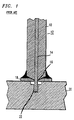
- Fig. 1 there is illustrated the prior art Columbia University design.
- the cladding 10 as the end of a single mode optical fiber 12 is removed to expose the core 14.
- the exposed core of the fiber is inserted through an opening 16 in a precision machined aluminum guide 18 which is coupled securely via epoxy cement or the like to a chip 20.
- the exposed end of the fiber projects into an opening 22 of the chip for coupling to, for example, a buried detector.
- the single mode optical fiber 12 is secured to the aluminum guide 18 with an adhesive such as epoxy cement.
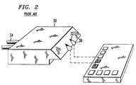
- Fig. 2 illustrates the prior art Honeywell design.
- an alignment fixture 30 contains a plurality of chemically machined grooves 32, each being adapted to receive and hold an optical fiber 34.
- the ends 36 of the optical fibers are held captive by the grooves which are beveled to permit light in the core of a fiber to be reflected out at a desired angle.
- the bevel has an angle of 45°, the light will leave the fiber at an angle 90° to the axis of the core.
- the Honeywell design can be used to couple an array of optical fibers aligned in a single plane to integrated detectors 38 located along a perimeter of a chip or a board.
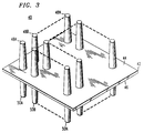
- a support member 42 having opposing surfaces 44, 46 supports a first 48 and second 50 array of pillars.
- the first array of pillars consist of discrete pillars 48A, 48B, 48C... 48N; and the second array of pillars consist of discrete pillars 50A, 50B, 50C ... 50N.
- the various pillars 48A ... 48N which project outward from surface 44 are optically aligned with corresponding pillars 50A... 50N which project outward from opposing surface 52.
- the pillars operate as optical fibers where the lengths of each optical fiber is the length of pillar 48N plus the length of pillar 50N plus the thickness of the support member 42.
- the pillars can be formed by micromachining, using either a laser, ion milling, chemical etching, injection molding or the like.
- micromachined as used herein with respect to an array of pillars which project outward from opposing surfaces of a support member, is to be construed to mean a structure which is configured using any process which can produce the inventive structure with a high degree of dimensional and geometric accuracy.
- Materials which can be utilized to form the structure by etching includes, but is not limited to FotoformTM glass (obtained from Corning Glass).
- Fotoform material is photopatternable via exposure to UV light and subsequent chemical etching. Pillars having lengths of six hundred microns, diameters of less than forty microns and spacings of less than fifty microns can be achieved using this material.
- the processed glass is transparent and transmits optical energy.
- Fotoform material can be processed to form the inventive device by, first, exposing either one or both surfaces of a plate of Fotoform to ultraviolet (UV) light through a high precision mask.
- the mask forms a desired pattern of UV light on a ground and polished surface of a plate of Fotoform glass.
- the exposed plate is heat treated to develop the pattern.
- the areas of the glass that was exposed to the UV light becomes a semi-crystalline, glass-ceramic material that is 30 to 50 times more soluble in a dilute hydrofluoric acid solution than the nonexposed parts of the glass. This solubility differences enables the exposed pattern to be differentially etched.
- Fotoform has the property that when exposed to ultraviolet light (UV), silver atoms form crystallization centers in the exposed regions, which during a subsequent heat treatment allow nucleation and growth of lithium metasilicate crystals. Once this heat treatment is completed, the regions which were exposed to UV are 30-40 times more soluble in dilute hydrofluoric acid than unexposed regions.
- An optical connective device was formed by exposing a plate 1.6 mm thick to plane-wave UV normally incident through a standard photolithographic mask with small opaque disks. Upon heating to 600°C, the regions exposed to UV crystallize. The plate is then exposed to agitated HF causing fast etching of the crystallized regions from both faces leaving pillars.
- the etch was timed so as to leave a 170 ⁇ m thick supporting member.
- the pillars were each approximately 700 ⁇ m long.
- the resulting pillar tips were roughened by the etch, so mechanical polishing was performed.
- the fibers were supported by wax that was melted and flowed between the fibers and allowed to cool. The entire fabrication process was performed with negligible variations across a 4x4 inch plate.
- the end of the pillars can be shaped to have a lens rather than being flat.
- One method of producing a lens is to heat the ends of the pillars until the material starts to melt and form a convex shaped lens.
- Pillars whose tips have a diameter of nominally 40,60,80 and 100 ⁇ m and arrays with center-to-center spacings of 400 and 1000 ⁇ m have been fabricated.
- the inventive connect device can also be formed by using LexanTM OQ-1020 from General Electric. This method is an optically transmitting plastic which, in combination with the injection molding process, forms a one-piece molded device. During the molding process, care should be exercised to insure that all bubbles have been eliminated from the finished product.
- a wax-like material can be melted and poured onto each surface and allowed to solidify. This wax-like material provides mechanical support to the various pillars so that they will resist flexing or bending. Thereafter, the ends of the optical fibers are ground to a final dimension and polished. If desired, the wax-like material may remain after the grinding and polishing operation provided it has an index of refraction which is less than that of pillar material. If desired the ends of the optical fibers can be shaped to form a convex lens by either heating or shaping during the molding process. If the lens is formed during the molding process, it can be either concave or convex.
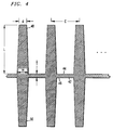
- Fig. 4 there is illustrated an enlarged cross section view through a row of pillars 48N, 50N and support member 42 of Fig. 3 when formed with Fotoform material.
- the acid solution first removes the material from the very ends of the fibers being formed.
- the acid solution is in contact with the ends of the fibers for a larger period of time then it is in contact with the base of the fibers coupled to the support member 42.
- the optical fibers become slightly tapered as illustrated in Fig. 4.
- the dimension C which is the center-to-center spacing of the optical fibers is 400 microns; the dimension d, which is the final face diameter of the optical fiber is 40 microns; the dimension m, which is the mask feature diameter is 100 microns; the dimension L, which is the stub length of the optical fiber length is 600 microns; and, the dimension t, which is the thickness of the support member, is 250 microns.
- the closest center-to-center spacing of the optical fibers which can be obtained is d+2L tan (3°) + 10 microns which, for our device, is roughly 112 microns.
- the dimension of 3° in the relationship is the taper angle of the pillar.
- a layer resistance glass is positioned between two layers of Fotoform.
- the etch resistant glass can have a thickness of 250 microns and each sheet of Fotoform can have a thickness of 600 microns.
- Thermal bonding or an adhesive of epoxy or the like can be used to attach the two sheets of Fotoform to the etch resistant glass.
- the sandwich assemblage is then exposed to UV light, heat treated and etched to form the inventive structure.
- structural support material such as wax or the like can be poured into the spaces between the optical fibers and allowed to harden to prevent the various optical fibers from bending or flexing during subsequent grinding and polishing steps.
- the inventive device disclosed is a simple to construct, zero-assembly, two dimensional optical fiber array connect device.
- it is a single piece of glass or plastic in which multimode optical fiber pillars have been either etched from both faces or formed with injection molding.
- the position of the pillars and, thus, the fibers, are defined by lithographic techniques or the like thus allowing the device to be aligned with integrated circuit chips.
- the inventive optical connective device here disclosed makes possible information access from the entire area of a chip, rather than just the perimeter, as light can flow vertically from the surface, and it does this with a connect device which is free of assemblage problems.
- optical inter-chip communication entails two-dimensional arrays of light beams.
- the construction of large two dimensional arrays of optical fiber connect devices required a painstaking and costly assemblage. Therefore, prior to this invention, efforts were focussed on free-space optical techniques which required complicated optical designs.
- an optical fiber interconnect device can be made which has optical fibers in two dimensions, not just one, and they are at the exact location needed for optical interconnection to a chip.
- connections to a chip or a board are not restricted to an end or edge, but can be along a side of a chip or board i.e., its major surface.
- chips or boards can now be stacked one on top of another, the inventive connect device being interposed between adjacent chip or boards to provide the necessary connections between the various chips or boards of a stack.
- the use of the invention devices between chips allows a cooling fluid to flow therebetween, if desired.
Landscapes
- Physics & Mathematics (AREA)
- General Physics & Mathematics (AREA)
- Optics & Photonics (AREA)
- Optical Couplings Of Light Guides (AREA)
Claims (13)
- Un dispositif de connexion optique comprenantun élément de support (42) ayant des première et seconde surfaces opposées (44, 46),un premier réseau de piliers (48A, 48B, ..., 48N) supporté par la première surface (44) et s'étendant vers l'extérieur à partir de celle-ci,un second réseau de piliers (50A, 50B, ..., 50N) supportés par la seconde surface (46) et s'étendant vers l'extérieur à partir de celle-ci,les piliers du premier réseau de piliers étant alignés de façon optique avec des piliers correspondants du second réseau de piliers,les piliers du premier réseau et du second réseau et l'élément de support étant en un matériau qui est transparent pour l'énergie optique, de façon que l'énergie optique qui est reçue par un piller quelconque soit transmise à travers ce piller, à travers la partie de l'élément de support qui est couplée à l'extrémité de ce pilier, et ensuite à travers le pilier qui est aligné de façon optique avec le pilier qui a reçu l'énergie optique.
- Le dispositif de la revendication 1, dans lequel
le premier réseau de piliers et le second réseau de piliers sont positionnés dans une seule dimension. - Le dispositif de la revendication 1, dans lequel
le premier réseau de piliers et le second réseau de piliers sont positionnés dans deux dimensions. - Le dispositif de la revendication 1, dans lequel
le premier réseau de piliers, le second réseau de piliers et l'élément de support sont constitués par le même matériau. - Le dispositif de la revendication 1, dans lequel
le premier réseau de piliers et le second réseau de piliers sont des fibres optiques multimodes. - Le dispositif de la revendication 5,
comprenant en outre un matériau de support ayant un indice de réfraction qui est inférieur à l'indice de réfraction du premier réseau de piliers, ce matériau de support étant positionné entre les piliers du premier réseau de piliers. - Le dispositif de la revendication 5, dans lequel
les piliers du premier réseau de piliers et les piliers du second réseau de piliers ont des longueurs qui sont supérieures à leurs diamètres. - Le dispositif de la revendication 5, dans lequel les piliers du premier réseau de piliers ont un diamètre de bout qui est au moins de 35 micromètres.
- Le dispositif de la revendication 5, dans lequel les piliers du premier réseau de piliers ont un diamètre de bout d'au moins 60 micromètres.
- Le dispositif de la revendication 5, dans lequel le premier réseau de piliers, le second réseau de piliers et l'élément de support consistent en un matériau transparent pouvant être enlevé par attaque chimique.
- Le dispositif de la revendication 5, dans lequel le premier réseau de piliers et le second réseau de piliers consistent en un matériau transparent pouvant être enlevé par attaque chimique, et
l'élément de support est un matériau transparent qui ne peut pas être enlevé par attaque chimique. - Le dispositif de la revendication 5, dans lequel les piliers du premier réseau de piliers ont des extrémités qui sont planes.
- Le dispositif de la revendication 5, dans lequel les piliers du premier réseau de piliers ont des extrémités qui sont courbées.
Applications Claiming Priority (2)
| Application Number | Priority Date | Filing Date | Title |
|---|---|---|---|
| US07/785,352 US5170455A (en) | 1991-10-30 | 1991-10-30 | Optical connective device |
| US785352 | 1991-10-30 |
Publications (2)
| Publication Number | Publication Date |
|---|---|
| EP0540236A1 EP0540236A1 (fr) | 1993-05-05 |
| EP0540236B1 true EP0540236B1 (fr) | 1996-02-28 |
Family
ID=25135224
Family Applications (1)
| Application Number | Title | Priority Date | Filing Date |
|---|---|---|---|
| EP92309615A Expired - Lifetime EP0540236B1 (fr) | 1991-10-30 | 1992-10-21 | Dispositif de connexion optique |
Country Status (4)
| Country | Link |
|---|---|
| US (1) | US5170455A (fr) |
| EP (1) | EP0540236B1 (fr) |
| JP (1) | JPH07117630B2 (fr) |
| DE (1) | DE69208588T2 (fr) |
Families Citing this family (56)
| Publication number | Priority date | Publication date | Assignee | Title |
|---|---|---|---|---|
| IL98879A (en) * | 1991-07-18 | 1994-05-30 | Israel State | Junction between a circular and a rectangular waveguide |
| US5371822A (en) * | 1992-06-09 | 1994-12-06 | Digital Equipment Corporation | Method of packaging and assembling opto-electronic integrated circuits |
| US5274730A (en) * | 1992-11-05 | 1993-12-28 | At&T Bell Laboratories | Optical interconnection of photonic circuits |
| US5928819A (en) * | 1996-12-19 | 1999-07-27 | Xerox Corporation | Methods to fabricate optical equivalents of fiber optic face plates using reactive liquid crystals and polymers |
| US6160606A (en) * | 1997-08-05 | 2000-12-12 | Xerox Corporation | Optical equivalents of fiber optic face plates using irradiation sensitive glass |
| SE519767C2 (sv) * | 1997-11-26 | 2003-04-08 | Volvo Car Corp | Förbränningssystem |
| US6972436B2 (en) * | 1998-08-28 | 2005-12-06 | Cree, Inc. | High voltage, high temperature capacitor and interconnection structures |
| US6246076B1 (en) | 1998-08-28 | 2001-06-12 | Cree, Inc. | Layered dielectric on silicon carbide semiconductor structures |
| US6403286B1 (en) | 1999-11-04 | 2002-06-11 | Corning Incorporated | High aspect ratio patterning of glass film |
| US6519393B2 (en) * | 2000-08-10 | 2003-02-11 | Bruce Lee Booth | Coupling of optical waveguide to optical waveguide devices |
| US6956238B2 (en) | 2000-10-03 | 2005-10-18 | Cree, Inc. | Silicon carbide power metal-oxide semiconductor field effect transistors having a shorting channel and methods of fabricating silicon carbide metal-oxide semiconductor field effect transistors having a shorting channel |
| US6767843B2 (en) | 2000-10-03 | 2004-07-27 | Cree, Inc. | Method of N2O growth of an oxide layer on a silicon carbide layer |
| US6610366B2 (en) | 2000-10-03 | 2003-08-26 | Cree, Inc. | Method of N2O annealing an oxide layer on a silicon carbide layer |
| US7067176B2 (en) | 2000-10-03 | 2006-06-27 | Cree, Inc. | Method of fabricating an oxide layer on a silicon carbide layer utilizing an anneal in a hydrogen environment |
| WO2002050584A2 (fr) * | 2000-12-21 | 2002-06-27 | Biovalve Technologies, Inc. | Systemes de reseaux de micro-aiguilles |
| US6528373B2 (en) * | 2001-02-12 | 2003-03-04 | Cree, Inc. | Layered dielectric on silicon carbide semiconductor structures |
| US6956999B2 (en) | 2001-02-20 | 2005-10-18 | Cyberoptics Corporation | Optical device |
| US6443631B1 (en) | 2001-02-20 | 2002-09-03 | Avanti Optics Corporation | Optical module with solder bond |
| US20040212802A1 (en) | 2001-02-20 | 2004-10-28 | Case Steven K. | Optical device with alignment compensation |
| US6546172B2 (en) | 2001-02-20 | 2003-04-08 | Avanti Optics Corporation | Optical device |
| US6546173B2 (en) | 2001-02-20 | 2003-04-08 | Avanti Optics Corporation | Optical module |
| EP1412793A1 (fr) * | 2001-08-01 | 2004-04-28 | Infineon Technologies AG | Unite de couplage optique et procede pour inserer des guides d'ondes optiques dans une unite de couplage optique |
| WO2003027734A1 (fr) * | 2001-09-26 | 2003-04-03 | Shipley Company, Llc | Reseau de fibre optique a alignement angulaire de fibre variable et procede de fabrication de ce reseau |
| US7280985B2 (en) * | 2001-12-06 | 2007-10-09 | New York University | Logic arrangement, data structure, system and method for multilinear representation of multimodal data ensembles for synthesis, recognition and compression |
| US7022378B2 (en) * | 2002-08-30 | 2006-04-04 | Cree, Inc. | Nitrogen passivation of interface states in SiO2/SiC structures |
| US7221010B2 (en) * | 2002-12-20 | 2007-05-22 | Cree, Inc. | Vertical JFET limited silicon carbide power metal-oxide semiconductor field effect transistors |
| US6945708B2 (en) * | 2003-02-18 | 2005-09-20 | Jds Uniphase Corporation | Planar lightwave circuit package |
| US7074643B2 (en) * | 2003-04-24 | 2006-07-11 | Cree, Inc. | Silicon carbide power devices with self-aligned source and well regions and methods of fabricating same |
| US6979863B2 (en) * | 2003-04-24 | 2005-12-27 | Cree, Inc. | Silicon carbide MOSFETs with integrated antiparallel junction barrier Schottky free wheeling diodes and methods of fabricating the same |
| US7379925B2 (en) * | 2003-07-25 | 2008-05-27 | New York University | Logic arrangement, data structure, system and method for multilinear representation of multimodal data ensembles for synthesis, rotation and compression |
| US20050148289A1 (en) * | 2004-01-06 | 2005-07-07 | Cabot Microelectronics Corp. | Micromachining by chemical mechanical polishing |
| US7693299B2 (en) * | 2004-01-13 | 2010-04-06 | New York University | Method, system, storage medium, and data structure for image recognition using multilinear independent component analysis |
| US7727904B2 (en) * | 2005-09-16 | 2010-06-01 | Cree, Inc. | Methods of forming SiC MOSFETs with high inversion layer mobility |
| US7728402B2 (en) | 2006-08-01 | 2010-06-01 | Cree, Inc. | Semiconductor devices including schottky diodes with controlled breakdown |
| US8432012B2 (en) | 2006-08-01 | 2013-04-30 | Cree, Inc. | Semiconductor devices including schottky diodes having overlapping doped regions and methods of fabricating same |
| EP2631951B1 (fr) | 2006-08-17 | 2017-10-11 | Cree, Inc. | Transistors bipolaires haute puissance à grille isolée |
| US8835987B2 (en) | 2007-02-27 | 2014-09-16 | Cree, Inc. | Insulated gate bipolar transistors including current suppressing layers |
| US20090050774A1 (en) * | 2007-08-24 | 2009-02-26 | Poutous Menelaos K | Micro-optical bench and method of fabricating micro-optical bench |
| US8232558B2 (en) | 2008-05-21 | 2012-07-31 | Cree, Inc. | Junction barrier Schottky diodes with current surge capability |
| US8288220B2 (en) | 2009-03-27 | 2012-10-16 | Cree, Inc. | Methods of forming semiconductor devices including epitaxial layers and related structures |
| US8294507B2 (en) | 2009-05-08 | 2012-10-23 | Cree, Inc. | Wide bandgap bipolar turn-off thyristor having non-negative temperature coefficient and related control circuits |
| US8629509B2 (en) | 2009-06-02 | 2014-01-14 | Cree, Inc. | High voltage insulated gate bipolar transistors with minority carrier diverter |
| US8193848B2 (en) | 2009-06-02 | 2012-06-05 | Cree, Inc. | Power switching devices having controllable surge current capabilities |
| US8541787B2 (en) | 2009-07-15 | 2013-09-24 | Cree, Inc. | High breakdown voltage wide band-gap MOS-gated bipolar junction transistors with avalanche capability |
| US8354690B2 (en) | 2009-08-31 | 2013-01-15 | Cree, Inc. | Solid-state pinch off thyristor circuits |
| US9117739B2 (en) | 2010-03-08 | 2015-08-25 | Cree, Inc. | Semiconductor devices with heterojunction barrier regions and methods of fabricating same |
| US8415671B2 (en) | 2010-04-16 | 2013-04-09 | Cree, Inc. | Wide band-gap MOSFETs having a heterojunction under gate trenches thereof and related methods of forming such devices |
| US9142662B2 (en) | 2011-05-06 | 2015-09-22 | Cree, Inc. | Field effect transistor devices with low source resistance |
| US9029945B2 (en) | 2011-05-06 | 2015-05-12 | Cree, Inc. | Field effect transistor devices with low source resistance |
| US9984894B2 (en) | 2011-08-03 | 2018-05-29 | Cree, Inc. | Forming SiC MOSFETs with high channel mobility by treating the oxide interface with cesium ions |
| US9373617B2 (en) | 2011-09-11 | 2016-06-21 | Cree, Inc. | High current, low switching loss SiC power module |
| WO2013036370A1 (fr) | 2011-09-11 | 2013-03-14 | Cree, Inc. | Module d'alimentation à haute densité de courant comprenant des transistors à topologie améliorée |
| US8618582B2 (en) | 2011-09-11 | 2013-12-31 | Cree, Inc. | Edge termination structure employing recesses for edge termination elements |
| US8680587B2 (en) | 2011-09-11 | 2014-03-25 | Cree, Inc. | Schottky diode |
| US9640617B2 (en) | 2011-09-11 | 2017-05-02 | Cree, Inc. | High performance power module |
| US8664665B2 (en) | 2011-09-11 | 2014-03-04 | Cree, Inc. | Schottky diode employing recesses for elements of junction barrier array |
Family Cites Families (9)
| Publication number | Priority date | Publication date | Assignee | Title |
|---|---|---|---|---|
| US3421805A (en) * | 1965-01-06 | 1969-01-14 | Rowland Products Inc | Changing optical pattern display |
| US4106046A (en) * | 1977-01-26 | 1978-08-08 | Westinghouse Electric Corp. | Radiant energy sensor |
| US4812002A (en) * | 1986-10-24 | 1989-03-14 | Hitachi, Ltd. | Optical coupling device and method of making the same |
| US4895615A (en) * | 1988-03-09 | 1990-01-23 | Siemens Aktiengesellschaft | Monolithic fabrication techniques for front face optoelectronic couplers and/or optical components including ridge structured waveguides |
| US4874499A (en) * | 1988-05-23 | 1989-10-17 | Massachusetts Institute Of Technology | Electrochemical microsensors and method of making such sensors |
| JPH0215679A (ja) * | 1988-07-04 | 1990-01-19 | Ricoh Co Ltd | 実装方法 |
| GB2239323A (en) * | 1989-12-21 | 1991-06-26 | Plessey Co Plc | Optical waveguide stacks and assemblies connected to opto-electronic components |
| US5093879A (en) * | 1990-06-22 | 1992-03-03 | International Business Machines Corporation | Electro-optical connectors |
| US5093890A (en) * | 1990-11-27 | 1992-03-03 | International Business Machines Corporation | Optical bus for computer systems |
-
1991
- 1991-10-30 US US07/785,352 patent/US5170455A/en not_active Expired - Lifetime
-
1992
- 1992-10-19 JP JP4304500A patent/JPH07117630B2/ja not_active Expired - Fee Related
- 1992-10-21 DE DE69208588T patent/DE69208588T2/de not_active Expired - Fee Related
- 1992-10-21 EP EP92309615A patent/EP0540236B1/fr not_active Expired - Lifetime
Also Published As
| Publication number | Publication date |
|---|---|
| DE69208588D1 (de) | 1996-04-04 |
| US5170455A (en) | 1992-12-08 |
| JPH07117630B2 (ja) | 1995-12-18 |
| JPH06289259A (ja) | 1994-10-18 |
| EP0540236A1 (fr) | 1993-05-05 |
| DE69208588T2 (de) | 1996-09-26 |
Similar Documents
| Publication | Publication Date | Title |
|---|---|---|
| EP0540236B1 (fr) | Dispositif de connexion optique | |
| US10684419B2 (en) | Waveguide connector elements and optical assemblies incorporating the same | |
| US5218663A (en) | Optical waveguide device and method for connecting optical waveguide and optical fiber using the optical waveguide device | |
| JP3117708B2 (ja) | 光学システム | |
| US6496624B1 (en) | Optical waveguide device for optical wiring and manufacturing method therefor | |
| JPH1010362A (ja) | 受動的に調整されたファイバーを有する光集積回路 | |
| WO1992021047A1 (fr) | Procede de connexion d'un guide d'ondes optiques a une fibre optique | |
| KR20040015286A (ko) | 형성후 표식부 최적화 방법 | |
| JP2005352453A (ja) | 光ファイバ部品及び光導波路モジュール並びにこれらの製造方法 | |
| WO2009039652A1 (fr) | Sous-ensemble optique parallèle à deux substrats | |
| US11914193B2 (en) | Optical assembly for coupling with two-dimensionally arrayed waveguides and associated methods | |
| EP1253452A2 (fr) | Matrice de fibres optiques | |
| JP2005517966A (ja) | 高密度光ファイバーアレイ | |
| JPH02280104A (ja) | 接続端子台 | |
| JP3065300B2 (ja) | 光ファイバ及び光導波路素子の接続構造 | |
| EP1353205B1 (fr) | Alignement d'un assemblage de fibres utilisant des repères d'ajustage | |
| JPS61149905A (ja) | 光合分波器 | |
| US5280550A (en) | Method of coupling an optical fiber to an optoelectronic component and connector devices obtained thereby | |
| JP3833863B2 (ja) | 多チャネル光路変換部品及びその作製方法、ならびに多チャネルビームスプリッタ及びその作製方法 | |
| US6445837B1 (en) | Hybrid opto-electronic circuits and method of making | |
| WO2004010191A1 (fr) | Raccordement a une face arriere optique | |
| US20060193560A1 (en) | Coupling structure between a fiber and a planar lightwave circuit (PLC) and manufacturing method therefor | |
| US20230054219A1 (en) | Optical assembly for interfacing waveguide arrays, and associated methods | |
| TW200304557A (en) | Ceramic waferboard | |
| JP2008164943A (ja) | 多チャンネル光路変換素子およびその作製方法 |
Legal Events
| Date | Code | Title | Description |
|---|---|---|---|
| PUAI | Public reference made under article 153(3) epc to a published international application that has entered the european phase |
Free format text: ORIGINAL CODE: 0009012 |
|
| AK | Designated contracting states |
Kind code of ref document: A1 Designated state(s): DE FR GB IT |
|
| 17P | Request for examination filed |
Effective date: 19931021 |
|
| RAP3 | Party data changed (applicant data changed or rights of an application transferred) |
Owner name: AT&T CORP. |
|
| 17Q | First examination report despatched |
Effective date: 19950627 |
|
| GRAA | (expected) grant |
Free format text: ORIGINAL CODE: 0009210 |
|
| AK | Designated contracting states |
Kind code of ref document: B1 Designated state(s): DE FR GB IT |
|
| REF | Corresponds to: |
Ref document number: 69208588 Country of ref document: DE Date of ref document: 19960404 |
|
| ET | Fr: translation filed | ||
| ITF | It: translation for a ep patent filed | ||
| PLBE | No opposition filed within time limit |
Free format text: ORIGINAL CODE: 0009261 |
|
| 26N | No opposition filed | ||
| PGFP | Annual fee paid to national office [announced via postgrant information from national office to epo] |
Ref country code: FR Payment date: 20000918 Year of fee payment: 9 |
|
| PGFP | Annual fee paid to national office [announced via postgrant information from national office to epo] |
Ref country code: GB Payment date: 20000921 Year of fee payment: 9 |
|
| PGFP | Annual fee paid to national office [announced via postgrant information from national office to epo] |
Ref country code: DE Payment date: 20001229 Year of fee payment: 9 |
|
| PG25 | Lapsed in a contracting state [announced via postgrant information from national office to epo] |
Ref country code: GB Free format text: LAPSE BECAUSE OF NON-PAYMENT OF DUE FEES Effective date: 20011021 |
|
| REG | Reference to a national code |
Ref country code: GB Ref legal event code: IF02 |
|
| GBPC | Gb: european patent ceased through non-payment of renewal fee |
Effective date: 20011021 |
|
| PG25 | Lapsed in a contracting state [announced via postgrant information from national office to epo] |
Ref country code: FR Free format text: LAPSE BECAUSE OF NON-PAYMENT OF DUE FEES Effective date: 20020628 |
|
| PG25 | Lapsed in a contracting state [announced via postgrant information from national office to epo] |
Ref country code: DE Free format text: LAPSE BECAUSE OF NON-PAYMENT OF DUE FEES Effective date: 20020702 |
|
| REG | Reference to a national code |
Ref country code: FR Ref legal event code: ST |
|
| PG25 | Lapsed in a contracting state [announced via postgrant information from national office to epo] |
Ref country code: IT Free format text: LAPSE BECAUSE OF NON-PAYMENT OF DUE FEES;WARNING: LAPSES OF ITALIAN PATENTS WITH EFFECTIVE DATE BEFORE 2007 MAY HAVE OCCURRED AT ANY TIME BEFORE 2007. THE CORRECT EFFECTIVE DATE MAY BE DIFFERENT FROM THE ONE RECORDED. Effective date: 20051021 |