EP0540285A2 - Procédé et dispositif pour la normalisation des nombres à virgule flottante - Google Patents
Procédé et dispositif pour la normalisation des nombres à virgule flottante Download PDFInfo
- Publication number
- EP0540285A2 EP0540285A2 EP92309814A EP92309814A EP0540285A2 EP 0540285 A2 EP0540285 A2 EP 0540285A2 EP 92309814 A EP92309814 A EP 92309814A EP 92309814 A EP92309814 A EP 92309814A EP 0540285 A2 EP0540285 A2 EP 0540285A2
- Authority
- EP
- European Patent Office
- Prior art keywords
- normalisation
- floating point
- mantissa
- result
- data
- Prior art date
- Legal status (The legal status is an assumption and is not a legal conclusion. Google has not performed a legal analysis and makes no representation as to the accuracy of the status listed.)
- Withdrawn
Links
Images


Classifications
-
- G—PHYSICS
- G06—COMPUTING OR CALCULATING; COUNTING
- G06F—ELECTRIC DIGITAL DATA PROCESSING
- G06F5/00—Methods or arrangements for data conversion without changing the order or content of the data handled
- G06F5/01—Methods or arrangements for data conversion without changing the order or content of the data handled for shifting, e.g. justifying, scaling, normalising
- G06F5/012—Methods or arrangements for data conversion without changing the order or content of the data handled for shifting, e.g. justifying, scaling, normalising in floating-point computations
-
- G—PHYSICS
- G06—COMPUTING OR CALCULATING; COUNTING
- G06F—ELECTRIC DIGITAL DATA PROCESSING
- G06F5/00—Methods or arrangements for data conversion without changing the order or content of the data handled
- G06F5/01—Methods or arrangements for data conversion without changing the order or content of the data handled for shifting, e.g. justifying, scaling, normalising
- G06F5/015—Methods or arrangements for data conversion without changing the order or content of the data handled for shifting, e.g. justifying, scaling, normalising having at least two separately controlled shifting levels, e.g. using shifting matrices
Definitions
- This invention relates to a method and apparatus for performing certain floating point arithmetic operations in a data processing system. More particularly, the invention relates to an improved normalisation method and circuitry which reduces the amount of die size required for normalisation calculations.
- Floating point apparatus allow for improvements in the amount of time a data processing unit takes to perform arithmetic calculations.
- the standard specifies basic and extended floating point number formats, arithmetic operations, conversions between integer and floating point formats, conversions between different floating point formats, conversions between basic format floating point numbers and decimal strings, and the handling of certain floating point exceptions.
- a typical floating point arithmetic operation may be accomplished in either single precision or double precision format.
- Each of these formats utilises a sign, exponent and fraction/mantissa field, where the respective fields occupy predefined portions of the floating point number.
- the sign field is a single bit occupying the most significant bit position
- the exponent field is an 8-bit quantity occupying the next-most significant bit positions
- the mantissa field occupies the least significant 23-bit positions.
- the sign field is a single bit occupying the most significant bit position; the exponent field is an 11-bit field occupying the next-most significant bit positions; the mantissa field is a 52-bit field occupying the least significant bit positions.
- the second step of conventional floating point arithmetic is performed.
- This step perform the arithmetic operation specified, such as addition, subtraction, multiplication, division, etc. Both the exponent and mantissa fields are operated upon.
- the third traditional step is to normalise the data after the arithmetic operation. This step allows for maintaining the highest degree of precision of floating numbers, as is commonly known to those of ordinary skill in the art. In standard systems, this normalisation is accomplished by counting the number of leading zeroes contained in the resultant mantissa field. This count is then subtracted from the exponent field, and the mantissa field is shifted left by a similar count amount, resulting in a 'one' bit being in the most significant bit position of the mantissa field.
- bus width or data path
- Original central processor units or CPU's
- the bus widths have been increased in order to transfer more data in the same amount of time. This is desirable as, given a bus bandwidth that has a maximum transfer rate, only a given number of data exchanges can occur for a given time period.
- 16 bit buses such as the Intel 80286 microprocessor and 32 bit buses such as the Intel 80386 microprocessor, have become increasingly popular. Even larger bus widths are easily envisioned to be forthcoming in the near future.
- bus data width causes increases in the die size of the microprocessors, however.
- the die size is proportional to the overall manufacturing cost of a given integrated circuit component such as a microprocessor
- these higher bus width components result in a proportionally higher cost.
- the amount of functionality that can be placed on the integrated circuitry is reduced for devices that support these larger bus widths. This is because a 32 bit register takes approximately twice the die surface area of a 16 bit register.
- a 32 bit register takes approximately twice the die surface area of a 16 bit register.
- more integrated circuit components are required to maintain a given functionality.
- numerous integrated circuit components are required. This results in higher costs to the end user.
- the exponential portions of A and B are compared, substantially simultaneously with performing an arithmetic operation on the mantissa portions of A and B, to generate at least one prediction control signal, and a result of the arithmetic operation is normalised using the at least one prediction control signal.
- the normalising step comprises eliminating leading zero bit positions of the result of the arithmetic operation in a number of bit locations which number is less than the total mantissa width of the result, using the at least one prediction control signal, and then successively looping and eliminating leading zero bit positions until the highest order bit position is non-zero.
- Normalisation of floating point numbers may use a much smaller register width than would normally be required for the data operands which can be processed. As the register width is smaller, the number of circuits required to achieve the normalisation is reduced, resulting in a decrease in the chip area required to perform such operation.
- This aspect of the present invention entails streamlining of the normalisation circuitry to efficiently operate on the more prevalent type of data being presented to the floating point unit.
- the width of the registers required were substantially less than the width required for the less frequent data types and/or operations.
- the data is preferably broken into smaller portions and normalized using successive cycles of the normalisation circuitry.
- Certain data types and/or operations which occur relatively infrequently require multiple cycles of the normalisation function.
- a significant savings was realized in the number of circuits required to implement normalisation.
- the overall performance of the normalisation function is minimally impacted.
- considerable savings in integrated circuit real estate is achieved with minimal impact to the overall throughput of the system.
- Normalisation is accomplished in a first embodiment by comparing the exponential portions of the floating point numbers while the mantissa portions of the numbers are being arithmetically operated upon.
- the result of the exponent compare is used to pre-shift the result of the mantissa arithmetic operation by varying amounts up to 48 bits.
- This shifted result is then normalized using a 16 bit zero detect logic and a 16 bit shifter. These are physically very small circuits.
- up to 64 bits (48 bits from the 1st stage and 16 bits from the next stage) of leading zeros are detected and shifted out of the mantissa.
- the possibility of the datum being normalized in this cycle is high, so that almost all data can be normalized in a single pass.
- the leading bit of the intermediate result being zero signals the need for additional normalisation.
- the data will loop on the normalisation cycle to achieve additional normalisation. This costs one additional clock cycle for each 16 leading zeros beyond the first 64.
- the recycling is limited at 6 extra clocks, or cycles, to avoid infinite looping when a mantissa contains all zeros. Since the probability of needing an additional normalisation cycle is cut in half with each successive iteration, needing more than one additional cycle is extremely rare.
- datums having bit lengths of up to 161 bits in the preferred embodiment are normalized using circuitry which doesn't require concurrent operation on the full datum.
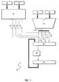
- Figure 1 is a functional block diagram of system flow and control in a system according to an embodiment of the invention.
- Figure 2 is a diagram indicating zero-fill during pre-alignment.
- Figure 3 is a detailed logical diagram of the data flow and control shown in Figure 1.
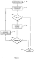
- Figure 4 is a state machine diagram for controlling the iterative looping for successive passes of normalisation.
- FIG. 1 shows the functional block diagram of the preferred embodiment of this invention.
- a floating point post-normalisation function 10 normalises floating point numbers conforming to ANSI/IEEE Standard No. 754-1985.
- An exponent compare circuit 12 has inputs from two floating point numbers A and B to be operated upon. The A exponent is shown at 14 and the B exponent portion is shown at 16, both being inputs to the exponent compare circuitry 12.
- This circuitry is able to predict, within 1 bit of accuracy, whether the resultant mantissa portion 24 calculated by the arithmetic unit 18 will require shifting of 48, 32, 16, or 0 bits.
- Four control lines are generated by this prediction portion 12, and are shown at 26, 28, 30, and 32 to represent the need to shift 48, 32, 16 or 0 bits respectively. As can be seen, these control lines 26, 28, 30, and 32 are used to shift at 34 the mantissa result 24 by the determined amount, and store this amount in result register 36.
- the mantissa result 24 is determined by the arithmetic unit 18, which operates on the mantissa portion of A at 20 and the mantissa portion B at 22 using conventional arithmetic circuitry commonly known to those of ordinary skill in the art.
- This result 24 is the portion of the floating point number requiring normalisation, which entails shifting out leading/most significant zeros and decrementing the resultant exponent by 1 for each zero bit shifted. This normalisation is desired to maintain the maximum degree of accuracy when operating on floating point numbers having dissimilar magnitudes.
- the exponent compare circuitry at 12 is able to predict the number of leading zeros which will result in the mantissa operation, within 1 bit, because of the following.
- the mantissa portions of A and B shown at 20 and 22 must be pre-aligned prior to performing 'addition-like' operations, so that the relative magnitudes of the numbers have some relationship to one another.
- the pre-alignment involves shifting in leading zeros into a mantissa and similarly changing the exponent portion to accommodate the shifted in values.
- the key feature of the exponent compare circuit at 12 is to analyse the initial exponent values of A and B prior to their being compensated due to the mantissa zero-fill.
- the result of the 'addition operation' 23 couples to block 24, which is an unnormalised result of the arithmetic operation.
- the number of leading zeros in this unnormalized result 24 is shown at 21, and will be +/- 1 of being the same number of leading zeros shown at 19.
- the +/- one bit uncertainty is due to whether or not the arithmetic operation caused a carry-in/carry-out, or ripple, bit.
- an accurate prediction can be made as to the number of resulting leading zeros in the unnormalised result 24 without having to interrogate/read the actual mantissa result itself.
- exponent compare/leading zero prediction operation 12 is performed substantially simultaneously, or in parallel with, the arithmetic operations occurring in block 18. Thus, this additional step of comparing exponent values to allow for leading zero prediction incurs no time delays/penalties.
- the data in the result register 36 is passed on to a sixteen bit zero detect and shift logic 38, where conventional techniques are used to determine the number of leading zeros, remove the leading zeros, and decrement the exponent an amount corresponding to the number of leading zeros which were removed. These techniques are well known to those of ordinary skill in the art, as illustrated by U.S. patent 4,941,120.
- the results of this detect/shift logic 38 are shown at 40 as the normalised datum.
- the leading bit of the resultant datum 40 is used to determine if further normalisation is required. If the leading bit of 40 is non-zero, no further normalisation is required, as the purpose of normalisation is to shift the datum bits until the most significant bit is a one. If the leading bit is zero, however, additional normalisation is required. The datum 40 will loop on the normalisation cycle to achieve additional normalisation. This costs one additional clock cycle for each 16 leading zeros beyond the first 64. In the preferred embodiment, the recycling is limited at 6 extra clocks, or cycles, to avoid infinite looping when a mantissa contains all zeros.
- the use control logic 26, 28, 30, and 32 in conjunction with the output of the arithmetic unit 18 as shown at 34 of Figure 1 is further detailed in Figure 3.
- the arithmetic result 24 is 161 bits wide in the preferred embodiment, and is indicated as W(0... 160).
- the data result is fed into a combinational logic circuit 42 which latches a result at 44, the latched result indicated as X(0...112), based upon the control signals 26, 28, 30, and 32.
- These control signals indicate whether the input W(0...160) should be shifted 48, 32, 16, or 0 bits respectively.
- X(0...112) is therefore the input value W(0...160) shifted by the number of bits as indicated by the control lines 26, 28, 30 and 32.
- X(0...112) is the number stored in the result register 36 of Figure 1.
- a multiplexor 56 of Figure 3 has four groups of inputs 48, 50, 52, and 54, and 4 select lines 62 which indicate which of the four input groups to pass to the multiplexor output 58.
- the first input group 48 is comprised of bits 0-100 of X(0...112).
- the second input group 50 is comprised of bits 4-104 of X(0...112), or in other words, X(0...112) shifted left by four bit positions.
- the third input group 52 is comprised of bits 8-108 of X(0...112), or in other words, X(0...112) shifted left by eight bit positions.
- the fourth input group 54 is comprised of bits 12-112 of X(0...112), or in other words, Y(0...112) shifted left by twelve bit positions.
- Control signals 62 are used to select which input group will be passed on at 58 to the next stage. These control signals 62 are generated by a conventional 2-4 bit decoder shown at 60.
- the input to this decoder 60 are control lines 64 which were generated by the logic at 46. This logic is a two-bit latch, and is determined by the first significant 12 bits of the resulting X(0...112). The two control lines thus have an encoded value indicating whether X(0...112) should be shifted 0, 4, 8 or 12 bits during the multiplexor stage 56.
- the output of multiplexor 56 is shown at 58 to be Y(0...100), which now contains the hex-normalized portion of the original data W(0...160).
- the third stage has a multiplexor 66 having five input groups 68, 70, 72, 74, and 76 and five select lines 78.
- the first input group 68 is comprised of bits 0-54 of Y(0...100).
- the second input group 70 is comprised of bits 1-53 of Y(0...100), or in other words, Y(0...100) shifted left by one bit positions.
- the third input group 72 is comprised of bits 2-54 of Y(0...100), or in other words, Y(0...100) shifted left by two bit positions.
- the fourth input group 74 is comprised of bits 3-57 of Y(0...100), or in other words, Y(0...100) shifted left by three bit positions.
- the fifth input group 76 is comprised of bits 4-58 of Y(0...100), or in other words Y(0...100) shifted left by four bit positions.
- Control signals 78 are used to select which input group will be passed on at 40 to the output. These control signals 78 are generated by a random logic 80, which is in turn driven by the four leading bits of Y(0...100), and which is indicated at 82 as Y(0...3). Conventional random logic 80 is used to generate control signals 78 based upon the definitions shown in Table 2.
- the first group 68 feeding multiplexor 66 will be selected if the most significant bit of Y is a one.
- the second group 70 of multiplexor 66 will be selected if the two most significant bits of Y are equal to '01'. Groups three through five are similarly selected based upon the most significant bits of Y.
- the resulting output 40 is the output value which has been selected by the random logic 80. This resulting output 40 is similarly shown in the functional diagram of Figure 1. This output is further passed to a rounding circuit shown at 84, which is a conventional rounder net germane to the present invention.
- control line 33 of block 42 is activated, signalling that a feedback cycle should occur. This signal 33 preempts the control signals 26, 28, 30, and 32, and indicates that block 42 should instead accept input latched at 92.
- the value contained in 92 consists of the most significant 53 bits out of the rounding circuit 84, indicated as R(0...52), concatenated with the least significant bits of output Y, indicated as Y(57...100), concatenated with sixteen binary zeros, indicated at x'0000' (i.e. four hex zeros). Again, this concatenated value is shown at 92 of Figure 3.
- R(0...52) is guaranteed to be the most significant bits of Z(0...52) because the control signal 94 of block 84, which indicates whether to add a zero or one to the input value, is forced to a zero by logic 88. This is accomplished as one of the input signals 90 to logic 88 is the feedback control line 33. Again, the other input signals 90 are of no significance to the current invention, as they are used during normal, conventional, rounding operations which are outside the scope of this invention.
- the resultant datum 40 is recycled to be stored in the result register 36.
- the detect/shift logic 38 analyses the most significant sixteen bits of this recycled result to determine the number of leading zeros to remove. As this is only a sixteen bit detection circuitry, only leading zero locations in the most significant sixteen bits can be detected.
- the entire value stored in the result register is then shifted by an amount, not exceeding sixteen bits in the preferred embodiment, as determined by the zero detect logic.
- the result of this detect/shift is again stored at datum result 40.
- the most significant bit of this datum result 40 is again used to determine whether continued looping is required, in a manner as previously described.
- This looping of the resultant datum 40 through the detect/shift logic 38 continues, up to a maximum of six loops in the preferred embodiment, until the most significant bit of the datum result is non-zero. When this is achieved, the post-normalisation function ends, as the resultant datum 40 has been properly normalised.
- This looping methodology/logic is further illustrated by a state machine in Figure 4.
- a state machine 100 At the beginning of this state machine 100, a three-bit counter is initialised. Then, the basic normalisation as earlier described regarding block 38 of Figure 1 occurs at 101 of Figure 4. Following up to sixteen bits of normalisation, a determination of whether additional normalisation is required is made in block 102, using the most significant bit of Z. If the most significant bit is a logical 'one', no further normalisation is required, and normalisation ends at 108. This is the most frequently occurring path. If the most significant bit is a logical 'zero' at 102, a counter is incremented at 104.
- the counter is then tested at 106, using conventional logic circuits, to determine if the counter has yet reached at value of six, which in the preferred embodiment is encoded as binary '110'. If this maximum value is reached, control passes out of the state machine at 108 with the resultant datum Z residing at 40 of Figures 1 and 3. If the three-bit counter is less than the threshold value, the feedback control signal 33 of Figure 1 is generated, indicating a need for looping the result 40 through the normalisation process. This signal generation is conceptually shown to occur in block 107 of Figure 4. This signal generation triggers a next successive pass through the normalisation circuitry of Figure 3 to generate a new value Z.
- This iterative looping provides a way to incrementally normalise a number having a significant number of leading zeros without having to provide detection and shift circuitry which supports the entire data path/width concurrently.
- a reduction in the amount of circuitry is obtained at the expense of requiring multiple cycle times for normalizing these worst case numbers.
Landscapes
- Engineering & Computer Science (AREA)
- Theoretical Computer Science (AREA)
- Physics & Mathematics (AREA)
- General Engineering & Computer Science (AREA)
- General Physics & Mathematics (AREA)
- Computing Systems (AREA)
- Complex Calculations (AREA)
Applications Claiming Priority (2)
| Application Number | Priority Date | Filing Date | Title |
|---|---|---|---|
| US78613691A | 1991-10-31 | 1991-10-31 | |
| US786136 | 2007-04-11 |
Publications (2)
| Publication Number | Publication Date |
|---|---|
| EP0540285A2 true EP0540285A2 (fr) | 1993-05-05 |
| EP0540285A3 EP0540285A3 (en) | 1993-08-11 |
Family
ID=25137689
Family Applications (1)
| Application Number | Title | Priority Date | Filing Date |
|---|---|---|---|
| EP19920309814 Withdrawn EP0540285A3 (en) | 1991-10-31 | 1992-10-27 | Method and apparatus for floating point normalisation |
Country Status (3)
| Country | Link |
|---|---|
| US (1) | US5384723A (fr) |
| EP (1) | EP0540285A3 (fr) |
| JP (1) | JPH05216620A (fr) |
Families Citing this family (16)
| Publication number | Priority date | Publication date | Assignee | Title |
|---|---|---|---|---|
| US5886915A (en) * | 1995-11-13 | 1999-03-23 | Intel Corporation | Method and apparatus for trading performance for precision when processing denormal numbers in a computer system |
| US5892697A (en) * | 1995-12-19 | 1999-04-06 | Brakefield; James Charles | Method and apparatus for handling overflow and underflow in processing floating-point numbers |
| US5742533A (en) * | 1996-05-21 | 1998-04-21 | International Business Machines Corporation | Method and apparatus for modulus error checking |
| US5856831A (en) * | 1996-06-12 | 1999-01-05 | Hewlett-Packard Company | Clamping system and method for clamping floating point color values from a geometry accelerator in a computer graphics system |
| US7043516B1 (en) * | 1998-03-13 | 2006-05-09 | Hewlett-Packard Development Company, L.P. | Reduction of add-pipe logic by operand offset shift |
| US7062657B2 (en) * | 2000-09-25 | 2006-06-13 | Broadcom Corporation | Methods and apparatus for hardware normalization and denormalization |
| US20020061107A1 (en) * | 2000-09-25 | 2002-05-23 | Tham Terry K. | Methods and apparatus for implementing a cryptography engine |
| US20020078342A1 (en) * | 2000-09-25 | 2002-06-20 | Broadcom Corporation | E-commerce security processor alignment logic |
| US8364734B2 (en) * | 2005-09-15 | 2013-01-29 | International Business Machines Corporation | Converting from decimal floating point into scaled binary coded decimal |
| US7698352B2 (en) * | 2005-09-15 | 2010-04-13 | International Business Machines Corporation | System and method for converting from scaled binary coded decimal into decimal floating point |
| US8051117B2 (en) | 2007-04-26 | 2011-11-01 | International Business Machines Corporation | Shift significand of decimal floating point data |
| US8190664B2 (en) * | 2007-04-26 | 2012-05-29 | International Business Machines Corporation | Employing a mask field of an instruction to encode a sign of a result of the instruction |
| US8051118B2 (en) * | 2007-04-26 | 2011-11-01 | International Business Machines Corporation | Composition of decimal floating point data |
| US20080270495A1 (en) * | 2007-04-26 | 2008-10-30 | International Business Machines Corporation | Insert/extract biased exponent of decimal floating point data |
| US8412760B2 (en) * | 2008-07-22 | 2013-04-02 | International Business Machines Corporation | Dynamic range adjusting floating point execution unit |
| US11188299B2 (en) * | 2019-07-31 | 2021-11-30 | International Business Machines Corporation | Repurposed hexadecimal floating point data path |
Family Cites Families (6)
| Publication number | Priority date | Publication date | Assignee | Title |
|---|---|---|---|---|
| JPS6017534A (ja) * | 1983-07-08 | 1985-01-29 | Mitsubishi Electric Corp | 浮動小数点数値正規化回路 |
| US4852039A (en) * | 1987-06-19 | 1989-07-25 | Digital Equipment Corporation | Apparatus and method for accelerating floating point addition and subtraction operations by accelerating the effective subtraction procedure |
| JP2695178B2 (ja) * | 1988-03-11 | 1997-12-24 | 富士通株式会社 | 演算回路 |
| US4969118A (en) * | 1989-01-13 | 1990-11-06 | International Business Machines Corporation | Floating point unit for calculating A=XY+Z having simultaneous multiply and add |
| US5157624A (en) * | 1990-12-13 | 1992-10-20 | Micron Technology, Inc. | Machine method to perform newton iterations for reciprocal square roots |
| US5220524A (en) * | 1990-12-13 | 1993-06-15 | Micron Technology, Inc. | Machine method to perform newton iterations for reciprocals |
-
1992
- 1992-08-13 JP JP4216059A patent/JPH05216620A/ja active Pending
- 1992-10-27 EP EP19920309814 patent/EP0540285A3/en not_active Withdrawn
-
1994
- 1994-02-28 US US08/205,123 patent/US5384723A/en not_active Expired - Fee Related
Also Published As
| Publication number | Publication date |
|---|---|
| EP0540285A3 (en) | 1993-08-11 |
| JPH05216620A (ja) | 1993-08-27 |
| US5384723A (en) | 1995-01-24 |
Similar Documents
| Publication | Publication Date | Title |
|---|---|---|
| US4758972A (en) | Precision rounding in a floating point arithmetic unit | |
| US4893268A (en) | Circuit and method for accumulating partial products of a single, double or mixed precision multiplication | |
| US5384723A (en) | Method and apparatus for floating point normalization | |
| KR100239029B1 (ko) | 가산기와 함께 사용하기 위한 결과 정규화기 및 결과 정규화 방법과 그를 포함하는 데이터 프로세서 | |
| US8166092B2 (en) | Arithmetic device for performing division or square root operation of floating point number and arithmetic method therefor | |
| EP0359809B1 (fr) | Procede et appareil de prevision de la normalisation de la virgule flottante | |
| US9256577B2 (en) | Apparatuses and related methods for overflow detection and clamping with parallel operand processing | |
| US5132925A (en) | Radix-16 divider using overlapped quotient bit selection and concurrent quotient rounding and correction | |
| EP0328619B1 (fr) | Appareil et procede d'utilisation d'une chaine de report unique permettant la detection du ''un'' en tete et la calcul du bit ''collant'' (''sticky '' bit) | |
| US7373369B2 (en) | Advanced execution of extended floating-point add operations in a narrow dataflow | |
| EP0416308A2 (fr) | Multiplieur pour des nombres à chiffres signés à structure matricielle rectangulaire | |
| US5408426A (en) | Arithmetic unit capable of performing concurrent operations for high speed operation | |
| US7290023B2 (en) | High performance implementation of exponent adjustment in a floating point design | |
| US6990505B2 (en) | Method/apparatus for conversion of higher order bits of 64-bit integer to floating point using 53-bit adder hardware | |
| US7725522B2 (en) | High-speed integer multiplier unit handling signed and unsigned operands and occupying a small area | |
| US20030140074A1 (en) | Leading Zero Anticipatory (LZA) algorithm and logic for high speed arithmetic units | |
| US5150319A (en) | Circuitry for rounding in a floating point multiplier | |
| CA2215719C (fr) | Detection des bits collants dans les systemes arithmetiques a virgule flottante | |
| US7016928B2 (en) | Floating point status information testing circuit | |
| US6988120B2 (en) | Arithmetic unit and method thereof | |
| US6976050B2 (en) | System and method for extracting the high part of a floating point operand | |
| US6615228B1 (en) | Selection based rounding system and method for floating point operations | |
| KR101922462B1 (ko) | 데이터 처리장치 및 이진수에 대해 시프트 기능을 수행하는 방법 | |
| US5867722A (en) | Sticky bit detector for a floating-point processor | |
| Li et al. | Design of a fully pipelined single-precision multiply-add-fused unit |
Legal Events
| Date | Code | Title | Description |
|---|---|---|---|
| PUAI | Public reference made under article 153(3) epc to a published international application that has entered the european phase |
Free format text: ORIGINAL CODE: 0009012 |
|
| AK | Designated contracting states |
Kind code of ref document: A2 Designated state(s): DE FR GB |
|
| PUAL | Search report despatched |
Free format text: ORIGINAL CODE: 0009013 |
|
| AK | Designated contracting states |
Kind code of ref document: A3 Designated state(s): DE FR GB |
|
| 17P | Request for examination filed |
Effective date: 19930819 |
|
| 18W | Application withdrawn |
Withdrawal date: 19960826 |