EP0540497A2 - Procédé de fabrication de dépôts solides de soudure - Google Patents
Procédé de fabrication de dépôts solides de soudure Download PDFInfo
- Publication number
- EP0540497A2 EP0540497A2 EP92890230A EP92890230A EP0540497A2 EP 0540497 A2 EP0540497 A2 EP 0540497A2 EP 92890230 A EP92890230 A EP 92890230A EP 92890230 A EP92890230 A EP 92890230A EP 0540497 A2 EP0540497 A2 EP 0540497A2
- Authority
- EP
- European Patent Office
- Prior art keywords
- solder
- die
- carrier part
- surface areas
- remelting
- Prior art date
- Legal status (The legal status is an assumption and is not a legal conclusion. Google has not performed a legal analysis and makes no representation as to the accuracy of the status listed.)
- Withdrawn
Links
Images
Classifications
-
- B—PERFORMING OPERATIONS; TRANSPORTING
- B23—MACHINE TOOLS; METAL-WORKING NOT OTHERWISE PROVIDED FOR
- B23K—SOLDERING OR UNSOLDERING; WELDING; CLADDING OR PLATING BY SOLDERING OR WELDING; CUTTING BY APPLYING HEAT LOCALLY, e.g. FLAME CUTTING; WORKING BY LASER BEAM
- B23K1/00—Soldering, e.g. brazing, or unsoldering
- B23K1/0008—Soldering, e.g. brazing, or unsoldering specially adapted for particular articles or work
- B23K1/0016—Soldering of electronic components
-
- H—ELECTRICITY
- H05—ELECTRIC TECHNIQUES NOT OTHERWISE PROVIDED FOR
- H05K—PRINTED CIRCUITS; CASINGS OR CONSTRUCTIONAL DETAILS OF ELECTRIC APPARATUS; MANUFACTURE OF ASSEMBLAGES OF ELECTRICAL COMPONENTS
- H05K3/00—Apparatus or processes for manufacturing printed circuits
- H05K3/30—Assembling printed circuits with electric components, e.g. with resistors
- H05K3/32—Assembling printed circuits with electric components, e.g. with resistors electrically connecting electric components or wires to printed circuits
- H05K3/34—Assembling printed circuits with electric components, e.g. with resistors electrically connecting electric components or wires to printed circuits by soldering
- H05K3/3465—Application of solder
- H05K3/3485—Application of solder paste, slurry or powder
-
- H—ELECTRICITY
- H05—ELECTRIC TECHNIQUES NOT OTHERWISE PROVIDED FOR
- H05K—PRINTED CIRCUITS; CASINGS OR CONSTRUCTIONAL DETAILS OF ELECTRIC APPARATUS; MANUFACTURE OF ASSEMBLAGES OF ELECTRICAL COMPONENTS
- H05K2203/00—Indexing scheme relating to apparatus or processes for manufacturing printed circuits covered by H05K3/00
- H05K2203/01—Tools for processing; Objects used during processing
- H05K2203/0104—Tools for processing; Objects used during processing for patterning or coating
- H05K2203/0113—Female die used for patterning or transferring, e.g. temporary substrate having recessed pattern
-
- H—ELECTRICITY
- H05—ELECTRIC TECHNIQUES NOT OTHERWISE PROVIDED FOR
- H05K—PRINTED CIRCUITS; CASINGS OR CONSTRUCTIONAL DETAILS OF ELECTRIC APPARATUS; MANUFACTURE OF ASSEMBLAGES OF ELECTRICAL COMPONENTS
- H05K2203/00—Indexing scheme relating to apparatus or processes for manufacturing printed circuits covered by H05K3/00
- H05K2203/02—Details related to mechanical or acoustic processing, e.g. drilling, punching, cutting, using ultrasound
- H05K2203/0278—Flat pressure, e.g. for connecting terminals with anisotropic conductive adhesive
-
- H—ELECTRICITY
- H05—ELECTRIC TECHNIQUES NOT OTHERWISE PROVIDED FOR
- H05K—PRINTED CIRCUITS; CASINGS OR CONSTRUCTIONAL DETAILS OF ELECTRIC APPARATUS; MANUFACTURE OF ASSEMBLAGES OF ELECTRICAL COMPONENTS
- H05K2203/00—Indexing scheme relating to apparatus or processes for manufacturing printed circuits covered by H05K3/00
- H05K2203/03—Metal processing
- H05K2203/0338—Transferring metal or conductive material other than a circuit pattern, e.g. bump, solder, printed component
-
- H—ELECTRICITY
- H05—ELECTRIC TECHNIQUES NOT OTHERWISE PROVIDED FOR
- H05K—PRINTED CIRCUITS; CASINGS OR CONSTRUCTIONAL DETAILS OF ELECTRIC APPARATUS; MANUFACTURE OF ASSEMBLAGES OF ELECTRICAL COMPONENTS
- H05K2203/00—Indexing scheme relating to apparatus or processes for manufacturing printed circuits covered by H05K3/00
- H05K2203/04—Soldering or other types of metallurgic bonding
- H05K2203/043—Reflowing of solder coated conductors, not during connection of components, e.g. reflowing solder paste
-
- H—ELECTRICITY
- H05—ELECTRIC TECHNIQUES NOT OTHERWISE PROVIDED FOR
- H05K—PRINTED CIRCUITS; CASINGS OR CONSTRUCTIONAL DETAILS OF ELECTRIC APPARATUS; MANUFACTURE OF ASSEMBLAGES OF ELECTRICAL COMPONENTS
- H05K3/00—Apparatus or processes for manufacturing printed circuits
- H05K3/30—Assembling printed circuits with electric components, e.g. with resistors
- H05K3/32—Assembling printed circuits with electric components, e.g. with resistors electrically connecting electric components or wires to printed circuits
- H05K3/34—Assembling printed circuits with electric components, e.g. with resistors electrically connecting electric components or wires to printed circuits by soldering
- H05K3/3465—Application of solder
- H05K3/3478—Application of solder preforms; Transferring prefabricated solder patterns
Definitions
- the invention relates to a device and a method for producing solid solder coatings on solderable surface areas of a carrier part, which are used for fastening mounting parts, for example surface-mounted components (SMD) by remelting, with a die on the surfaces corresponding to the solderable surface areas of the carrier part with solder is pre-coated, this pre-coated die is positioned on the carrier part so that the solder parts rest on the corresponding solderable surface areas, in the subsequent solder remelting process the solder wets the solderable surface areas of the carrier part and after the solder has solidified again, the die is removed from the carrier part.
- SMD surface-mounted components
- a method which uses a matrix for the transfer of solder parts, which consists of a base layer covered with a conductive layer, on which in turn a mask layer is applied which corresponds to the surface areas of the carrier part that can be soldered Contains corresponding recesses.
- solder parts By applying an electrical voltage to the conductor layer, the required solder parts are electrodeposited in these recesses and then applied to the carrier part by a remelting process.
- Disadvantages are the three-layer matrix and the very complex galvanic application of the solder.
- the invention solves this problem in that the die consists of a monolithic material. As a result, it can be produced in a simple manner and can be coated with solder paste with little effort, for example by means of screen printing or stencil printing.
- the die is made of a glass plate the size of the surface portion to be soldered and facilitates the positioning process on the printed circuit board, since the soldering points can be seen through the die.
- the remelting heat can be partially supplied to the solder by radiation (eg laser, IR radiator).
- the die contains flat recesses on the surface parts provided for the precoating. With such a shaped matrix, screen printing can be omitted and the pre-coating is carried out by simply filling the depressions with solder.
- Another embodiment of the invention provides that the recesses are produced by etching the monolithic material. As a result, the finest structures can be produced in the recesses, which in turn allows a high degree of miniaturization in the manufacture of the soldering points.
- One embodiment of the invention provides that the remelting heat is supplied to the die by hot air and passes from the die to the solder by conduction.
- the known method for heating has the advantage when using a die according to the invention that the thermal load on the circuit board remains limited, since the die absorbs most of the heat and releases it to the solder.
- the remelting heat can be partially supplied to the solder by radiation, for example by means of a laser or infrared radiator, according to a further embodiment of the invention.
- the soldering points are heated if possible, it offers the lowest heat load for the printed circuit board and during repair work, the already soldered components are not stressed at all.
- the die can be precoated with solder in pasty form using stencil printing. This method is particularly advantageous in the production of solder coatings on partial areas of a printed circuit board, for example when repairing assembled printed circuit boards.
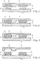
- FIG. 1 shows the cross section through the die already coated with solder or solder paste and the carrier body with surface areas wettable by the solder
- FIG. 2 shows the cross section through the die positioned on the carrier body
- FIG. 3 shows the cross section through the die and carrier body after remelting 4 and the cross section through the raised die and the carrier body, which is covered with a solder coating with a defined surface shape.
- the carrier body 4 shown in FIG. 1, for example a printed circuit board, has surface areas 3 wettable with solder at certain points in the form of solder points on the conductor tracks.
- the aim of the process is to coat these areas with Lot 2 in order to attach SMD components there as required.
- the surface shape of the solder points can be specified by using a die 1.
- the die 1 is pre-coated with solder or solder paste 2, for example in stencil printing.
- the precoating can also be carried out by filling flat recesses 5 in the die 1 with solder paste 2.
- the die 1 is positioned on the printed circuit board 4 (FIG. 2) and the solder or the solder paste 2 is heated to above the melting temperature (FIG. 3).
- the surface of the circuit board 4 is wetted with the solder 2 at the provided soldering points 3. After a cooling process, the die 1 is lifted off, the solder 2 remains on the printed circuit board 4 with a predetermined surface shape (FIG. 4).
- Now assembly parts for example SMD components, can be applied by remelting the solder 2 onto the printed circuit board, for example onto the conductor tracks 3, their positioning being facilitated by the flat surface shape of the solder points 2.
Landscapes
- Engineering & Computer Science (AREA)
- Mechanical Engineering (AREA)
- Manufacturing & Machinery (AREA)
- Microelectronics & Electronic Packaging (AREA)
- Electric Connection Of Electric Components To Printed Circuits (AREA)
Applications Claiming Priority (2)
| Application Number | Priority Date | Filing Date | Title |
|---|---|---|---|
| AT2145/91 | 1991-10-29 | ||
| AT214591 | 1991-10-29 |
Publications (2)
| Publication Number | Publication Date |
|---|---|
| EP0540497A2 true EP0540497A2 (fr) | 1993-05-05 |
| EP0540497A3 EP0540497A3 (en) | 1993-06-16 |
Family
ID=3528735
Family Applications (1)
| Application Number | Title | Priority Date | Filing Date |
|---|---|---|---|
| EP19920890230 Withdrawn EP0540497A3 (en) | 1991-10-29 | 1992-10-28 | Method of making solid solder coatings |
Country Status (2)
| Country | Link |
|---|---|
| EP (1) | EP0540497A3 (fr) |
| AU (1) | AU2739892A (fr) |
Cited By (3)
| Publication number | Priority date | Publication date | Assignee | Title |
|---|---|---|---|---|
| EP0797379A2 (fr) | 1996-03-18 | 1997-09-24 | KRONE Aktiengesellschaft | Panneau à circuit et procédé de montage et de soudage de composants électroniques en positions précises sur la surface du panneau à circuit |
| DE19716044A1 (de) * | 1997-04-17 | 1998-10-22 | Univ Dresden Tech | Verfahren zur Herstellung von festen Lotdepots auf Leiterplatten |
| US6042683A (en) * | 1996-10-10 | 2000-03-28 | Hagn; Erwin | Method and device for producing an aspiration surface on an object, and electrical component obtained thereby |
Family Cites Families (3)
| Publication number | Priority date | Publication date | Assignee | Title |
|---|---|---|---|---|
| FR1306699A (fr) * | 1961-09-04 | 1962-10-19 | Electronique & Automatisme Sa | Perfectionnement apporté à la réalisation des circuits électriques du genre dit |
| US4722470A (en) * | 1986-12-01 | 1988-02-02 | International Business Machines Corporation | Method and transfer plate for applying solder to component leads |
| US4832255A (en) * | 1988-07-25 | 1989-05-23 | International Business Machines Corporation | Precision solder transfer method and means |
-
1992
- 1992-10-28 EP EP19920890230 patent/EP0540497A3/de not_active Withdrawn
- 1992-10-28 AU AU27398/92A patent/AU2739892A/en not_active Abandoned
Cited By (4)
| Publication number | Priority date | Publication date | Assignee | Title |
|---|---|---|---|---|
| EP0797379A2 (fr) | 1996-03-18 | 1997-09-24 | KRONE Aktiengesellschaft | Panneau à circuit et procédé de montage et de soudage de composants électroniques en positions précises sur la surface du panneau à circuit |
| US6042683A (en) * | 1996-10-10 | 2000-03-28 | Hagn; Erwin | Method and device for producing an aspiration surface on an object, and electrical component obtained thereby |
| DE19716044A1 (de) * | 1997-04-17 | 1998-10-22 | Univ Dresden Tech | Verfahren zur Herstellung von festen Lotdepots auf Leiterplatten |
| DE19716044C2 (de) * | 1997-04-17 | 1999-04-08 | Univ Dresden Tech | Verfahren zum selektiven galvanischen Aufbringen von Lotdepots auf Leiterplatten |
Also Published As
| Publication number | Publication date |
|---|---|
| EP0540497A3 (en) | 1993-06-16 |
| AU2739892A (en) | 1993-05-06 |
Similar Documents
| Publication | Publication Date | Title |
|---|---|---|
| EP0528350B1 (fr) | Méthode de soudage et montage de composant sur plaquettes de circuits imprimés | |
| DE3784666T2 (de) | Verfahren und uebertragungsplatte zum auftragen von loetmittel auf kontaktbeine von bauteilen. | |
| DE69304911T2 (de) | Verfahren, vorrichtung und produkt für lötverbindungen bei oberflächenmontage. | |
| DE69727014T2 (de) | Ein Montierungsverfahren für eine Vielzahl elektronischer Teile auf einer Schaltungsplatte | |
| DE69204516T2 (de) | Leiterplatte mit Lötüberzug und Verfahren zu ihrer Herstellung. | |
| DE69207520T2 (de) | Elektrische Leiterplattenbaugruppe und Herstellungsverfahren für eine elektrische Leiterplattenbaugruppe | |
| DE4242408C2 (de) | Verfahren zum Verbinden eines Schaltkreissubstrates mit einem Halbleiterteil | |
| EP0487782B1 (fr) | Méthode de soudage de plaques de circuit | |
| DE102006004788A1 (de) | Halbleiterbauelement und Fertigungsverfahren für dieses | |
| DE102015107724A1 (de) | Verfahren zum Herstellen einer Substratanordnung, Substratanordnung, Verfahren zum Verbinden eines Elektronikbauteils mit einer Substratanordnung und Elektronikbauteil | |
| AT516750A4 (de) | Verfahren zur Voidreduktion in Lötstellen | |
| DE60207282T2 (de) | Verkapselung des anschlusslots zur aufrechterhaltung der genauigkeit der anschlussposition | |
| DE19511553C2 (de) | Verfahren zur Erzeugung elektrisch leitfähiger Strukturen, eine nach dem Verfahren erhaltene elektrisch leitfähige Struktur sowie Kombination zur Erzeugung elektrisch leitfähiger Strukturen | |
| DE4424831C2 (de) | Verfahren zur Herstellung einer elektrisch leitenden Verbindung | |
| EP0540497A2 (fr) | Procédé de fabrication de dépôts solides de soudure | |
| DE69009421T2 (de) | Verfahren zum Simultananordnen und Verlöten von SMD-Bauteilen. | |
| DE69705124T2 (de) | Umgekehrtes prägeverfahren | |
| DE2343235B2 (de) | Verfahren zur Befestigung und Kontaktierung von elektrischen Subminiatur-Bauelementen auf gedruckten Schaltungen | |
| EP3657914A1 (fr) | Plaque de circuit imprimé pour module led et méthode de sa manufacture | |
| EP0542149A2 (fr) | Procédé pour la production de domaines de soudure sur une plaquette à circuit imprimé et feuille à pâte de soudure pour la mise en oeuvre de ce procédé | |
| DE69523175T2 (de) | Mit einer einzigen lötlegierung kaschiertes substrat | |
| DE1465736B2 (de) | Funktionsblock, insbesondere für datenverarbeitende Anlagen | |
| DE3539318C2 (fr) | ||
| DE112004002603B4 (de) | Verfahren und Vorrichtung zum Löten von Bauteilen auf Leiterplatten mittels Lotformteilen | |
| DE2060933B2 (de) | Sockel fuer ein halbleiterbauelementgehaeuse und verfahren zu seiner herstellung |
Legal Events
| Date | Code | Title | Description |
|---|---|---|---|
| PUAI | Public reference made under article 153(3) epc to a published international application that has entered the european phase |
Free format text: ORIGINAL CODE: 0009012 |
|
| PUAL | Search report despatched |
Free format text: ORIGINAL CODE: 0009013 |
|
| AK | Designated contracting states |
Kind code of ref document: A2 Designated state(s): BE CH DE FR GB IT LI SE |
|
| AK | Designated contracting states |
Kind code of ref document: A3 Designated state(s): BE CH DE FR GB IT LI SE |
|
| 17P | Request for examination filed |
Effective date: 19930625 |
|
| 17Q | First examination report despatched |
Effective date: 19931130 |
|
| 18D | Application deemed to be withdrawn |
Effective date: 19940412 |