EP0540899B1 - UHF-Yagi-Antenne - Google Patents
UHF-Yagi-Antenne Download PDFInfo
- Publication number
- EP0540899B1 EP0540899B1 EP19920117301 EP92117301A EP0540899B1 EP 0540899 B1 EP0540899 B1 EP 0540899B1 EP 19920117301 EP19920117301 EP 19920117301 EP 92117301 A EP92117301 A EP 92117301A EP 0540899 B1 EP0540899 B1 EP 0540899B1
- Authority
- EP
- European Patent Office
- Prior art keywords
- antenna
- circuit board
- uhf
- circuit
- vhf
- Prior art date
- Legal status (The legal status is an assumption and is not a legal conclusion. Google has not performed a legal analysis and makes no representation as to the accuracy of the status listed.)
- Expired - Lifetime
Links
Images


Classifications
-
- H—ELECTRICITY
- H01—ELECTRIC ELEMENTS
- H01Q—ANTENNAS, i.e. RADIO AERIALS
- H01Q23/00—Antennas with active circuits or circuit elements integrated within them or attached to them
-
- H—ELECTRICITY
- H01—ELECTRIC ELEMENTS
- H01Q—ANTENNAS, i.e. RADIO AERIALS
- H01Q19/00—Combinations of primary active antenna elements and units with secondary devices, e.g. with quasi-optical devices, for giving the antenna a desired directional characteristic
- H01Q19/28—Combinations of primary active antenna elements and units with secondary devices, e.g. with quasi-optical devices, for giving the antenna a desired directional characteristic using a secondary device in the form of two or more substantially straight conductive elements
- H01Q19/30—Combinations of primary active antenna elements and units with secondary devices, e.g. with quasi-optical devices, for giving the antenna a desired directional characteristic using a secondary device in the form of two or more substantially straight conductive elements the primary active element being centre-fed and substantially straight, e.g. Yagi antenna
Definitions
- the invention relates to a UHF-Yagi antenna consisting of director elements, a reflector and a dipole.
- a Yagi antenna is already known from German Offenlegungsschrift No. 21 38 384, the known antenna being implemented in the manner of printed circuit technology and in particular in stripline technology.
- a room antenna for different frequency ranges is already known from German Offenlegungsschrift No. 24 53 164 and from the catalog "Kathrein catalog receive antennas 1990" (page 29, antenna BZX 20).
- This antenna is used to receive UHF and VHF, the UHF antenna being designed as a Yagi antenna.
- a dielectric circuit board is arranged, which receives an amplifier, switches and other electronic components. The amplifier is thus separated from the Yagi antenna by a distance that corresponds to the height of the standpipe of the Yagi antenna.
- a miniature television antenna is already known from German Offenlegungsschrift No. 2 146 182 (corresponding to US Patent 3, 707, 681).
- This known antenna has a first insulating substrate (11) on which the electrical components of the antenna are printed and a second insulating substrate (77) on which the components of the amplifier (40) are attached.
- the insulating substrate (77) with the components of the amplifier is held by a holder arm (76) which rigidly attaches the amplifier circuit to the lower housing part (62).
- the antenna and amplifier are therefore not arranged on the same substrate (circuit board); rather, in the vicinity of the substrate (11) on which the electrical components of the antenna are printed, the substrate (77 is fastened via the holding arm 76), the substrates (11) and (77) being separated from one another by a space.
- These constructive measures are apparently aimed at electromagnetically decoupling the antenna and amplifier.
- Electromagnetic decoupling proves to be critical, especially with Yagi antennas, because of the possible interaction between amplifier and antenna reflector.
- This arrangement known from German Offenlegungsschrift No. 2 146 182 is initially associated with the disadvantage that two different substrates, namely the substrate (11) for the actual antenna and the substrate (77) for the amplifier circuit, are used.
- the invention has for its object to provide a UHF Yagi antenna of the type mentioned, which enables a compact structure.
- a UHF-Yagi antenna consists of director elements, reflector and dipole, the director elements and the dipole consisting of conductor tracks. printed on a dielectric circuit board, and wherein a first Amplifier circuit is connected to the conductor tracks forming the dipole.
- the first amplifier circuit and the conductor tracks forming the dipole are arranged on the same circuit board in close proximity to one another and on the same side of the circuit board.
- the reflector is concavely curved and the first amplifier circuit is arranged between the dipole and the reflector.
- the arrangement of the amplifier and the conductor tracks on the same circuit board reduces the dimensions of the antenna and improves its electrical properties. At the same time, the manufacture of the antenna is simplified since the antenna elements and, for example, conductor tracks of the amplifier circuit can be applied to the circuit board in one operation.
- the concavely curved design of the reflector makes it possible to arrange an amplifier circuit in the space between the reflector and the dipole. This results in a compact structure and favorable electrical properties.
- By arranging the amplifier circuit in the immediate vicinity of the antenna a maximum of the energy absorbed by the antenna is used.
- a cable for connecting the UHF antenna and amplifier is not required. Mismatches and switch-on or fade-in losses are avoided, which occur when using a longer connecting line or a cable between the antenna and amplifier could result.
- the antenna according to the invention with the integrated amplifier circuit has a gain of 31 ⁇ 2 dB.
- a further advantageous embodiment is characterized in that a second amplifier circuit is arranged on the circuit board and has a connection for a VHF antenna in the form of two rods. This antenna can be installed by the consumer without the need for assembly tools.
- An antenna according to the invention in which the circuit board can be rotated, enables the antenna to be perfectly aligned in the directions of the signals to be received.
- Another embodiment of the antenna according to the invention in which the first and second amplifier circuits are followed by a mixer circuit which mixes UHF and VHF signals, is distinguished by the advantage that the UHF and VHF signals are provided in mixed form at the output thereof, whereby only one cable has to be provided for both the UHF antenna and the VHF antenna.
- the mixer circuit can be arranged on the circuit board, with which the advantages mentioned of reducing the dimensions of the overall arrangement and simplifying its assembly can be achieved to a greater extent.
- an antenna in which the circuits arranged on the circuit board are at least partially implemented in stripline technology and / or in SMD technology. This facilitates the manufacture of the overall arrangement antenna and associated electronic circuits, by printing the conductor tracks of the antenna and simultaneously printing the circuit structure of the circuits in a single process.
- the reflector consists of a double, metallic rod which forms a plane which is arranged approximately at right angles to the circuit board.
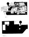
- FIG. 1 shows the position of a dielectric plate or circuit board 1 within a housing 2.
- the dielectric plate is in an inclined position of 2 degrees with respect to the horizontal plane defined by the foot part 21 of the housing 2.
- Director elements and the dipole of a UHF-Yagi antenna are arranged on the plate 1.
- the director elements and / or the dipole are formed by conductor tracks 11 which are printed on the plate 1.
- the plate 1 with the conductor tracks 11 either faces the upper part 22 of the housing 2 or the lower part 21 of the housing 2.
- the first three conductor tracks 111, 112 and 113 form the director elements and the two following conductor tracks 114 and 115 form the dipole.
- the reflector of the antenna is formed by a metal strip 12 which is arranged in a plane perpendicular to the plane in which the conductor tracks 111, 112, 113, 114 and 115 are arranged.
- the reflector can also be formed by a conductor track which is printed on the plate 1 (FIG. 2). At least one UHF amplifier circuit is arranged between the printed conductor tracks 11 and the reflector 12, as will be described with reference to FIG. 2.
- the housing 2 consists of a lower part 21 and an upper part 22.
- the shape of the housing 2 is slightly curved.
- Both parts 21 and 22 of the housing have mechanical connecting elements such as, for example, fastening pins, which enable the housing to be opened and closed easily.
- the plate 1 can be rotated in a plane parallel to the antenna base.
- the housing 2 can be connected to a carrier system 3, which is formed, for example, by a ball socket, the upper edge 31 of which is inserted into a circular groove 221 which is arranged in the lower part 21 of the housing 2 and which rotates with respect to the fixed carrier 3 allowed.
- the housing 2 is fastened to the carrier 3 by means of a screw which is inserted into an opening 32 in the base of the carrier 3, engages in a thread in a tube 212 arranged in the part 21 of the housing and extends up to within the carrier 3 whose lower base extends.
- a screw which is inserted into an opening 32 in the base of the carrier 3, engages in a thread in a tube 212 arranged in the part 21 of the housing and extends up to within the carrier 3 whose lower base extends.
- In the upper part 22 of the housing 2 there are two openings 221 into which a VHF antenna can be inserted. This consists of two rods, for example telescopic rods, which are described with reference to FIG. 7.
- the entire supply system can be arranged in the carrier 3, while a first amplifier circuit and optionally a second amplifier circuit are arranged on the plate 1 (FIG. 2).
- Figure 2 shows a schematic representation of the antenna and the associated electronic circuits. It should be noted that Figure 2 does not show the actual dimensions.
- the electronic circuit arrangements shown in FIG. 2 are at least partially implemented in microstrip technology and / or in SMD (Surface Mounting Devices) technology, so that the dimensions can be reduced very much, with an area of 75 mm in the specific embodiment ⁇ 35 mm is claimed.
- SMD Surface Mounting Devices
- the conductor tracks 111, 112, 113 and 114 have a width of approximately 3.5 mm; the conductor track 115 has a width of approximately 5 mm.
- the conductor track 111 has a length of approximately 107 mm; tracks 112 and 113 have a length of approximately 122 mm and tracks 114 and 115 have a length of approximately 92 mm and 76 mm, respectively.
- the approximate distances between the conductor tracks are as follows: the distance between the conductor tracks 111 and 112 is approximately 35 mm, the distance between the conductor tracks 112 and 113 is 16 mm and the distance between the conductor tracks 113 and 114 is 35 mm.
- the angle between tracks 114 and 115 is approximately 20 degrees.
- the reflector 12 has a parabolic shape and consists either of a conductor track which is arranged on the plate 1 (FIG. 1) or of a metal strip 12 which is in a plane perpendicular to the plane of the conductor tracks 111, 112, 113, 114, 115 is arranged.
- the conductor track has a width of approximately 3.5 mm, while the metal strip has an approximate height of 10 mm and a thickness of 0.4 mm.
- the length of the reflector (points E and F) is approximately 280 mm.
- the distance between the center of the dipole (conductor tracks 114, 115, point C) and the vertex of the parabola of the reflector (point D) is approximately 80 mm.
- the conductor tracks are made of copper, which is printed on a plate made of fiberglass. Another embodiment of the reflector is shown in FIG.
- FIG. 2 shows a first amplifier circuit which amplifies the UHF signals received by the antenna.
- a bandpass filter is arranged, which for example consists of the capacitors C23, C24, C25, C26 and C27 with 18 pF, 470pF, 1pF, 33 pF and 2.7 pF and coils L1 and L3 with 20 nH and 18 nH.
- This bandpass filter matches the impedance of the UHF antenna to the impedance of the first stage of the first amplifier circuit.
- the antenna impedance is approximately 300 ohms.
- the first amplifier consists of two transistors T1 (type NE68133 NEC) and T2 (type BFR 93A Philips). These transistors form two stages, which are matched and tuned to one another in a frequency range from 470 to 860 MHz, and cause an increase in the gain within the desired frequency band (470-860 MHz), whereby the signals are suppressed outside the frequency band.
- the first stage of the UHF amplifier is not powered with the aim of not degrading the noise characteristic, which noise characteristic is less than 2 dB.
- the second stage of the UHF amplifier is fed in order to compensate for the difference in gain as a function of the frequency generated in the first stage. This achieves a flat characteristic in the entire useful frequency range (470 - 860 MHz).
- the first amplifier circuit consists, for example, of the following components: a circuit for polarizing the transistor T1, which consists of the resistors R10, R14 and R15 with 560 ohms, 37 kiloohms and 3.3 kilohms, from a circuit for polarizing the transistor T2, which consists of resistors R7, R8, R9 and R12 with the values 470 ohms, 470 ohms, 18 kilohms and 10 kilohms; from a feedback circuit to transistor T2, which consists of resistors R11 and R13 with the values 220 ohms and 15 ohms and from the capacitors C14 and C17 with 22 pF and 470 pF, respectively, from high-pass filters consisting of the capacitor C9 and the coil L8 with 180 pF or 11nH consists of the capacitor C13 and the coil L7 with 4.7 pF or 10 nH and finally a high-
- FIG. 2 also shows a second amplifier circuit which amplifies the VHF signals received by the VHF antenna (FIG. 7).
- this amplifier which is connected directly to the VHF antenna (point I)
- a notch filter that blocks FM signals (87-108 MHz) and a low pass.
- the notch filter consists of the capacitors C29, C22, C30, C31 and C32 with the values 3.9 pF, 15 pF, 120 pF, 120 pF and 1.5 pF
- the low-pass filter consists of the coil L2 with 32 nH and the capacitor C33 with 8.2 pF.
- This low-pass filter makes it possible to match the impedance of the VHF antenna to the impedance of the second amplifier.
- the impedance of the VHF antenna is approximately 300 ohms.
- the second amplifier consists of a transistor T3 (type BFR93A Philips). This transistor is fed back in order to obtain a flat characteristic in the frequency range of 47-230 MHz.
- the second amplifier circuit consists of the following components: a polarization circuit consisting of resistors R4, R16, R2 and R1 with 470 ohms, 470 ohms, 22 kilohms and 10 kilohms, a feedback circuit consisting of resistors R3, R5 and R6 with 2.2 kilohms, 47 ohms and 10 ohms, and from the capacitors C2, C3 and C4 with 470 pF, 270 pF and 680 pF and from a high-pass filter consisting of the capacitor C6 with 34 pF.
- FIG. 2 also shows a VHF / UHF mixer circuit which consists of two printed filters, a high pass at the output of the UHF amplifier (point J), consisting of the capacitors C10 and C11 with 3.3 pF and 4.7 pF and from the coil L9 with 6 nH and from a low pass at the output of the VHF amplifier (point K), consisting of the coils L11 and L10 with 22 nH each and from the capacitors C5, C7, C28 with 18 pF, 22 pF and 1.8 pF.
- the output of the mixing circuit (point L) is connected to a low-loss cable (not shown in FIG. 2), via which the VHF and UHF signals are routed to an output selection circuit, which is arranged inside the carrier 3 (FIG. 1) is.
- the VHF and UHF amplifiers are also supplied via this cable.
- a Balum or symmetry circuit which consists of a coil L1.
- This circuit simulates a transmission path of ⁇ / 2 and transforms the symmetrical impedance of the dipole into the asymmetrical impedance inherent in the first amplifier.
- the circuit is implemented in printed copper on the plate of the UHF antenna itself and implemented together with the other circuits (amplifier, mixer circuit) between the dipole and the reflector of the antenna. It has an impedance transformation ratio of 1/4.
- the input point 0 of the first amplifier (base of the transistor T1) is arranged in the immediate vicinity of the point G of the output of the UHF antenna. This distance depends only on the geometric dimensions of the possible electronic components that are connected between the points G and O. In the present embodiment, this distance depends on the dimensions of the capacitors C26 and C24 and the coil L2. In the specific embodiment, the capacitors are implemented using SMD technology and the inductance L2 is printed on the circuit board in such a way that the geometric dimensions of the overall arrangement (C26, C24, L2) are reduced to a few millimeters.
- the first amplifier circuit and the arrangement of the other electronic circuits are arranged between the dipole (conductor tracks 114, 115) and the reflector 12.
- the dimensions of the overall arrangement of antenna and electronic circuits and of the housing are thus reduced.
- the electrical properties of the overall arrangement of antenna and electronic circuits are improved by the spatial proximity of electronic circuits and antenna and the correspondingly short connection path.
- Amplifier and reflector are electromagnetically decoupled in the arrangement structure described.
- the output selection switch consists of a switch INT, with which the signals which are supplied by the UHF and VHF antennas (point L) and the signals which are supplied by a possible external antenna (point M) via an in the carrier 3 ( Figure 1) arranged connecting element, are supplied.
- the output selection circuit includes diodes D2, D3, D4 and D5, each type 1N4148. By means of the switch INT in the "Y" position, the diodes D2, D4 and D5 are turned on, while the diode D3 is blocked.
- the signal at the "RF out” output (point N) is that coming from the indoor antenna (point L).
- the diodes D2, D4 and D5 are blocked, while the diode D3 conducts.
- the signal at the "F out” output (point N) is that coming from the external antenna (point M).
- connection to a terminal is established via the "RF out" output (point N).
- the power supply source consists of a transformer TRF 137218, a diode bridge PD (diodes type B125) and capacitors C1, C2, C3, C4 and C5 with the values 47 nF, 47 nF, 1000 uF, 47 nF and 47 nF and through the diode D1 (type IN4001).
- the power supply source has an input for 220 volts AC or 12 volts DC.
- This feed source feeds the electronic circuits shown in FIG. 2. From point L (FIG. 2) to point L (FIG. 3) the supply takes place by means of a connecting cable not shown in the figures. In particular, the same connecting cable is used for this purpose, which is used for the transmission of the VHF-UHF signals coming from point L (FIG. 2).
- the plate 1 with the printed conductor tracks 11, 112, 113, 114 and 115 is shown in perspective.
- the figure also shows the configuration of the reflector 12, which in the present embodiment consists of the metallic tape which is arranged in a plane perpendicular to the plane which has the conductor tracks 111, 112, 113, 114 and 115.
- the side of the circuit board 1 shown in FIG. 5 is connected to the lower housing part 21 (FIG. 1) and the side of the circuit board 1 shown in FIG. 6 is connected to the upper housing part 22 (FIG. 1).
- FIG. 5 and 6 represents the relatively large area of the mass (Ms) with respect to the dimensions of the circuit board.
- the part of the circuit board shown in FIGS. 5 and 6 has an area of 75 mm ⁇ , for example, as already described 35 mm.
- This configuration of the grounding mass (Ms) helps to keep the impedance between the different ground points (FIG. 2) of the circuits essentially constant with regard to the frequency range used. Avoiding currents induced via the mass reduces the risk of oscillations of the amplifier or amplifiers arranged between the dipole and the reflector.
- coils L1-L12 are shown in FIG. 5, which are implemented in printed circuit technology. These coils realized in the plane of the circuit board generate an electromagnetic field arranged in such a way as to the reflector, which leads to an electromagnetic decoupling of the amplifier and reflector contributes and reduces the risk of oscillations of the amplifier.
- FIG. 7 shows a possible system for the plug connection with the VHF antenna consisting of two telescopic rods.
- the assembly of the VHF antenna is reduced to the simple insertion of the rods into the housing openings and can be carried out by the consumer without the need for knowledge and assembly tools.
- FIG. 8 shows a further embodiment of the antenna according to the invention.
- This also consists of director elements 109A, 110A, 111A, 112A, 113A, a reflector 12A and a dipole 114A, 115A.
- the director elements consist of those shown in FIG Embodiment of conductor tracks 109A, 110A, 111A, 112A, 113A, which are printed on a circuit board 1A.
- the dipole of this embodiment consists of both traces 114A printed on the circuit board 1A and a metallic bar 115A arranged in a plane perpendicular to the plane of the circuit board 1A with the dipole traces.
- This metallic rod 115A is bent at its end regions by approximately 90 degrees and is connected at points D 'to the dipole conductor tracks 114A.
- the reflector consists of a double metal rod 12A, which is arranged in a plane perpendicular to the plane of the circuit board 1A.
- This reflector fulfills a double function; it forms the reflector of the UHF antenna and at the same time the dipole of the VHF antenna.
- a UHF amplifier is in turn arranged on the circuit board 1A between the dipole and the reflector.
- a VHF amplifier is also arranged on the circuit board 1A and connected to the reflector 12A at points G '. With this arrangement, the UHF reflector also takes on the function of the VHF dipole.
Landscapes
- Variable-Direction Aerials And Aerial Arrays (AREA)
- Aerials With Secondary Devices (AREA)
- Details Of Aerials (AREA)
- Transmitters (AREA)
Description
- Die Erfindung bezieht sich auf eine UHF-Yagi-Antenne, bestehend aus Direktorelementen, einem Reflektor und einem Dipol.
- Eine Yagi-Antenne ist bereits aus der deutschen Offenlegungsschrift Nr. 21 38 384 bekannt, wobei die bekannte Antenne in der Art der gedruckten Schaltungstechnik und insbesondere in Streifenleitertechnik realisiert ist.
- Eine Zimmerantenne für verschiedene Frequenzbereiche ist bereits aus der deutschen Offenlegungsschrift Nr. 24 53 164 und aus dem Katalog "Kathrein Katalog Empfangsantennen 1990", (Seite 29, Antenne BZX 20) bekannt.
Diese Antenne dient dem Empfang von UHF und VHF, wobei die UHF-Antenne als Yagi-Antenne ausgebildet ist. Im unteren Teil des Antennengehäuses ist eine dielektrische Schaltungsplatine angeordnet, die einen Verstärker, Weichen und weitere elektronische Bauelemente aufnimmt. Der Verstärker ist damit von der Yagi-Antenne um eine Entfernung getrennt angeordnet, die der Höhe des Standrohrs der Yagi-Antenne entspricht. - Aus der deutschen Offenlegungsschrift Nr. 2 146 182 (entsprechend US-Patent 3, 707, 681) ist bereits eine Miniatur-Fernsehantenne bekannt. Diese bekannte Antenne weist ein erstes isolierendes Substrat (11) auf, auf dem die elektrischen Bestandteile der Antenne aufgedruckt sind, und ein zweites isolierendes Substrat (77), auf dem die Bauteile des Verstärkers (40) befestigt sind. Das isolierende Substrat (77) mit den Bauteilen des Verstärkers wird von einem Halterarm (76) gehalten, der die Verstärkerschaltung starr an dem unteren Gehäuseteil (62) befestigt. Antenne und Verstärker sind also nicht auf demselben Substrat (Schaltungsplatte) angeordnet sind; vielmehr ist in der Nähe des Substrats (11), auf dem die elektrischen Bestandteile der Antenne aufgedruckt sind, das Substrat (77 über den Halterarm 76) befestigt, wobei die Substrate (11) und (77) durch einen Zwischenraum voneinander getrennt sind. Diese konstruktiven Maßnahmen sind offenbar darauf gerichtet, Antenne und Verstärker elektromagnetisch zu entkoppeln. Eine elektromagnetische Entkopplung erweist sich insbesondere bei Yagi-Antennen wegen der möglichen Wechselwirkung von Verstärker und Antennenreflektor als kritisch.
Diese aus der deutschen Offenlegungsschrift Nr. 2 146 182 bekannte Anordnung ist zunächst mit dem Nachteil verbunden, daß zwei verschiedene Substrate, nämlich das Substrat (11) für die eigentliche Antenne und das Substrat (77) für die Verstärkerschaltung verwendet werden. Damit ist die Herstellung von Antenne und Verstärker (unter anderem die Zubereitung der Substrate, Aufdrucken der Leiterbahnen, Bohren von Kontaktlöchern, Bestücken mit Bauelementen) für zwei Substrate, also voneinander getrennt vorzusehen. Dies bedeutet einen vergleichsweise großen Arbeitsaufwand.
Zudem ist bei dieser vorbekannten Antenne eine gesonderte Befestigung des Substrats 77 (mittels des Halterarms 76) vorzusehen. - Aus IEEE TRANSACTIONS ON CONSUMER ELECTRONICS; Bd. 22, Nr. 2, Mai 1976, New York US, Seiten 159 - 165; GIBSON ET WILSON "THE MINI-STATE - A SMALL TELEVISION ANTENNA" ist bereits eine Anordnung bekannt, die aus einer UHF-Yagi-Antenne und aus einer VHF-Antenne besteht (Seiten 164/165, Figur 8). Die bekannte Anordnung umfaßt auch eine Verstärkerschaltung. Der Reflektor der UHF-Yagi-Antenne besteht aus einem gerade geformten Leitungsstück (Figur 8, "UHF REFLECTOR").
Aus EP-A-0 346 125 ist bereits eine als "Microwave integrated apparatus for satellite broadcasting receiver" benannte Anordnung bekannt, wobei eine Antenne und ein Verstärker auf demselben Substrat angeordnet sein können. - Der Erfindung liegt die Aufgabe zugrunde, eine UHF-Yagi-Antenne der eingangs genannten Art zu schaffen, die einen kompakten Aufbau ermöglicht.
- Diese Aufgabe wird erfindungsgemäß mit den Merkmalen des Patentanspruchs 1 gelöst. Vorteilhafte Ausgestaltungen der erfindungsgemäßen Antennen sind Gegenstand der Unteransprüche.
- Eine erfindungsgemäße UHF-Yagi-Antenne besteht aus Direktorelementen, Reflektor und Dipol, wobei die Direktorelemente und der Dipol aus Leiterbahnen bestehen. die auf einer dielektrischen Schaltungsplatte gedruckt sind, und wobei eine erste Verstärkerschaltung mit den den Dipol bildenden Leiterbahnen verbunden ist. Die erste Verstärkerschaltung und die den Dipol bildenden Leiterbahnen sind auf derselben Schaltungsplatte in unmittelbarer Nähe zueinander und auf derselben Seite der Schaltungsplatte angeordnet. Dabei ist der Reflektor konkav gekrümmt und die erste Verstärkerschaltung ist zwischen dem Dipol und dem Reflektor angeordnet.
- Durch die Anordung des Verstärkers und der Leiterbahnen auf derselben Schaltungsplatte werden die Abmessungen der Antenne verringert und deren elektrische Eingenschaften verbessert. Zugleich wird die Herstellung der Antenne vereinfacht, da die Antennenelemente und beispielsweise Leiterbahnen der Verstärkerschaltung in einem Arbeitsgang auf die Schaltungsplatte aufgebracht werden können.
- Die konkav gekrümmte Ausbildung des Reflektors ermöglicht es, in dem Raum zwischen Reflektor und Dipol eine Verstärkerschaltung anzuordnen. Hierdurch werden ein kompakter Aufbau und günstige elektrische Eigenschaften erzielt. Durch die Anordnung der Verstärkerschaltung in unmittelbarer Nähe der Antenne wird ein Maximum der von der Antenne aufgenommenen Energie genutzt. Ein Kabel zur Verbindung von UHF- Antenne und Verstärker ist nicht erforderlich. Fehlanpassungen und Einschalt- bzw. Einblendverluste werden vermieden, die sich bei Verwendung einer längeren Verbindungsleitung bzw. eines Kabels zwischen Antenne und Verstärker ergeben könnten. Die erfindungsgemäße Antenne mit der integrierten Verstärkerschaltung weist einen Gewinn von 31 ± 2 dB auf.
- Eine weitere vorteilhafte Ausführungsform ist dadurch gekennzeichnet, daß auf der Schaltungsplatte eine zweite Verstärkerschaltung angeordnet ist und einen Anschluß für eine VHF-Antenne in Form zweier Stäbe aufweist. Eine Montage dieser Antenne kann vom Verbraucher vorgenommen werden, ohne daß Kenntnisse hierfür noch Montagewerkzeuge erforderlich sind.
- Im Hinblick auf die elektromagnetische Entkopplung von Verstärker und Antenne erweist es sich als vorteilhaft, daß auf der Schaltungsplatte im Bereich der ersten Verstärkerschaltung eine metallische Erdungsschicht mit einer auf diesen Bereich bezogenen, großen Fläche angeordnet ist.
- Eine erfindungsgemäße Antenne, bei der die Schaltungsplatte einer Drehbewegung zugänglich ist, ermöglicht die perfekte Ausrichtung der Antenne in die Richtungen der zu empfangenden Signale.
- Eine weitere Ausführungsform der erfindungsgemäßen Antenne, bei der der ersten und zweiten Verstärkerschaltung eine Mischerschaltung nachgeschaltet ist, die UHF- und VHF-Signale mischt, zeichnet sich durch den Vorteil aus, daß an deren Ausgang die UHF- und VHF-Signale gemischt bereitgestellt werden, wodurch nur ein Kabel und zwar sowohl für die UHF-Antenne alsauch für die VHF-Antenne vorzusehen ist.
- In diesem Zusammenhang kann die Mischerschaltung auf der Schaltungsplatte angeordnet sein, womit die erwähnten Vorteile der Abmessungsreduzierung der Gesamtanordnung und ihrer vereinfachten Montage in einem erweiteren Umfang erzielt werden.
- Bedeutende Vorteile werden bei einer Antenne erzielt, bei der die auf der Schaltungsplatte angeordneten Schaltungen mindestens teilweise in Streifenleitertechnik und/oder in SMD-Technik realisiert sind. Dies erleichert die Herstellung der Gesamtanordnung aus Antenne und zugehörigen elektronischen Schaltungen, indem das Drucken der Leiterbahnen der Antenne und das gleichzeitige Drucken der Schaltungsstruktur der Schaltungen in einem einzigen Prozess erfolgt.
- Der Vorteil eines größeren Antennengewinns ergibt sich, wenn der Reflektor aus einem gedoppelt ausgeführten, metallischen Stab besteht, der eine Ebene bildet, die in etwa rechtwinklig zur Schaltungsplatte angeordnet ist.
- Im folgenden wird die Erfindung anhand der Zeichnungen beispielhaft beschrieben.
Es zeigt - Figur 1
- einen Schnitt durch die in einem Gehäuse angeordnete erfindungsgemäße Antenne,
- Figur 2
- die Antenne in Verbindung mit einer ersten Verstärkerschaltung,
- Figur 3
- eine Ausgangsauswahlschaltung und eine Speiseschaltung für die erfindungsgemäße Antenne,
- Figur 4
- eine perspektivische Ansicht einer möglichen Gestaltung des Antennenreflektors,
- Figur 5
- die Ausgestaltung eines Teils der Schaltungsplatte im Bereich der Verstärkerschaltung(en) auf der den Verstärkerbauelementen bzw. den Antennenleiterbahnen zugewandten Seite der Schaltungsplatte,
- Figur 6
- die Ausgestaltung dieses Teils der Schaltungsplatte auf der den Verstärkerbauelementen bzw. den Antennenleiterbahnen abgewandten Seite der Schaltungsplatte,
- Figur 7
- ein System zur Anschaltung der VHF-Antenne, und
- Figur 8
- die perspektivische Darstellung der erfindungsgemäßen Antenne mit einer weiteren Ausführungsform des Reflektors.
- Figur 1 zeigt die Position einer dielektrischen Platte bzw. schaltungsplatine 1 innerhalb eines Gehäuses 2. Die dielektrische Platte befindet sich in einer geneigten Position von 2 Grad bezüglich der durch den Fußteil 21 des Gehäuses 2 definierten horizontalen Ebene. Auf der Platte 1 sind Direktorelemente und der Dipol einer UHF-Yagi-Antenne angeordnet.
Die Direktorelemente und/oder der Dipol sind durch Leiterbahnen 11 gebildet, die auf die Platte 1 gedruckt sind.
Die Platte 1 ist mit den Leiterbahnen 11 entweder dem den oberen Teil 22 des Gehäuses 2 zugewandt oder dem unteren Teil 21 des Gehäuses 2. In Figur 1 bilden die ersten drei Leiterbahnen 111, 112 und 113 die Direktorelemente und die zwei folgenden Leiterbahnen 114 und 115 bilden den Dipol.
Der Reflektor der Antenne wird durch ein Metallband 12 gebildet, das in einer Ebene senkrecht zu der Ebene angeordnet ist, in der die Leiterbahnen 111, 112, 113, 114 und 115 angeordnet sind. - Der Reflektor kann ebenfalls durch eine Leiterbahn gebildet sein, die auf die Platte 1 aufgedruckt ist (Figur 2). Zwischen den gedruckten Leiterbahnen 11 und dem Reflektor 12 ist mindestens eine UHF-Verstärkerschaltung angeordnet, wie anhand der Figur 2 beschrieben wird.
- Das Gehäuse 2 besteht aus einem unteren Teil 21 und einem oberen Teil 22. Die Form des Gehäuses 2 ist leicht gewölbt. Beide Teile 21 und 22 des Gehäuses weisen mechanische Verbindungselemente wie beispielsweise Befestigungszapfen auf, die ein leichtes Öffnen und Verschließen des Gehäuses ermöglichen.
- Die Platte 1 läßt sich in einer Ebene parallel zur Antennenbasis drehen. Das Gehäuse 2 kann mit einem Trägersystem 3 verbunden sein, das beispielsweise durch eine Kugelpfanne gebildet wird, deren oberer Rand 31 in eine kreisförmige Nut 221 eingeführt wird, die im unteren Teil 21 des Gehäuses 2 angeordnet ist und die dessen Drehung gegenüber dem festen Träger 3 erlaubt.
- Die Befestigung des Gehäuses 2 mit dem Träger 3 erfolgt mittels einer Schraube, die in eine Öffnung 32 in der Basis des Trägers 3 eingeführt wird, in ein Gewinde in einem im Teil 21 des Gehäuses angeordneten Rohr 212 eingreift und sich innerhalb des Trägers 3 bis zu dessen unterer Basis erstreckt.
Im oberen Teil 22 des Gehäuses 2 sind zwei Öffnungen 221 vorhanden, in die eine VHF-Antenne einführbar ist. Diese besteht aus zwei Stäben, beispielsweise Teleskopstäbe, die anhand der Figur 7 beschrieben werden. - Im Träger 3 kann das gesamte Speisungssystem angeordnet sein, während eine erste Verstärkerschaltung und gegebenenfalls eine zweite Verstärkerschaltung auf der Platte 1(Figur 2) angeordnet sind.
- Figur 2 zeigt eine schematische Darstellung der Antenne und der zugehörigen elektronischen Schaltungen. Es ist darauf hinzuweisen, daß Figur 2 nicht die tatsächlichen Dimensionen zeigt. Die in Figur 2 dargestellten elektronischen Schaltungsanordnungen sind bei der konkreten Ausführungsform mindestens teilweise in der Mikrostriptechnik und/oder in SMD (Surface Mounting Devices)-Technik realisiert, so daß die Abmessungen sehr verkleinert werden können, wobei bei der konkreten Ausführungsform eine Fläche von 75 mm × 35 mm beansprucht wird.
- Die Leiterbahnen 111, 112, 113 und 114 haben eine Breite von ungefähr 3,5 mm; die Leiterbahn 115 hat eine Breite von ungefähr 5 mm. Die Leiterbahn 111 hat eine Länge von ungefähr 107 mm; die Leiterbahnen 112 und 113 haben eine Länge von ungefähr 122 mm und die Leiterbahnen 114 und 115 haben eine Länge von ungefähr 92 mm bzw. 76 mm.
Die ungefähren Abstände zwischen den Leiterbahnen sind folgende: der Abstand zwischen den Leiterbahnen 111 und 112 beträgt ungefähr 35 mm, der Abstand zwischen den Leiterbahnen 112 und 113 beträgt 16 mm und der Abstand zwischen den Leiterbahnen 113 und 114 beträgt 35 mm. Der Winkel zwischen den Leiterbahnen 114 und 115 beträgt ungefähr 20 Grad. - Der Reflektor 12 hat eine parabolische Form und besteht entweder aus einer Leiterbahn, die auf der Platte 1 (Figur 1) angeordnet ist, oder aus einem Metallband 12, das in einer Ebene senkrecht zu der Ebene der Leiterbahnen 111, 112, 113, 114, 115 angeordnet ist.
- Die Leiterbahn hat eine Breite von ungefähr 3,5 mm, während das Metallband eine ungefähre Höhe von 10 mm und eine Dicke von 0,4 mm aufweist. Die Länge des Reflektors (Punkte E und F) beträgt ungefähr 280 mm.
- Der Abstand zwischen dem Zentrum des Dipols (Leiterbahnen 114, 115, Punkt C) und dem Scheitelpunkt der Parabel des Reflektors (Punkt D) beträgt ungefähr 80 mm.
Die Leiterbahnen sind in Kupfer ausgeführt, das auf einer Platte aus Fiberglas aufgedruckt ist.
Eine weitere Ausführungsform des Reflektors ist in Figur 8 dargestellt. - In Figur 2 ist eine erste Verstärkerschaltung dargestellt, die die von der Antenne empfangenen UHF-Signale verstärkt.
- Am Eingang dieses Verstärkers, der direkt mit der Antenne verbunden ist (Punkt G), ist ein Bandpaßfilter angeordnet, das beispielsweise aus den Kondensatoren C23, C24, C25, C26 und C27 mit 18 pF, 470pF, 1pF, 33 pF und 2,7 pF und Spulen L1 und L3 mit 20 nH und 18 nH besteht. Dieses Bandpaßfilter paßt die Impedanz der UHF-Antenne an die Impedanz der ersten Stufe der ersten Verstärkerschaltung an.
Die Impedanz der Antenne beträgt ungefähr 300 Ohm. - Der erste Verstärker besteht aus zwei Transistoren T1 (Typ NE68133 NEC) und T2 (Typ BFR 93A Philips). Diese Transistoren bilden zwei Stufen, die in einem Frequenzbereich von 470 bis 860 MHZ zueinander angepaßt und abgestimmt sind, und bewirken eine Steigerung des Gewinns innerhalb des gewünschten Frequenzbandes (470-860 MHz), wobei die Signale außerhalb des Frequenzbandes unterdrückt werden.
- Die erste Stufe des UHF-Verstärkers wird nicht gespeist mit dem Ziel, die Rauschcharakteristik nicht zu verschlechtern, wobei diese Rauschcharakteristik geringer als 2 dB ist. Die zweite Stufe des UHF-Verstärkers ist dagegen gespeist, um die Differenz des Gewinns in Abhängigkeit von der in der ersten Stufe erzeugten Frequenz zu kompensieren.
Damit wird eine ebene Charakteristik im gesamten Nutzfrequenzbereich (470 - 860 MHz) erzielt. - Die erste Verstärkerschaltung besteht beispielsweise aus den folgenden Komponenten: aus einer Schaltung zur Polarisation des Transistors T1, welche aus den Widerständen R10, R14 und R15 mit 560 Ohm, 37 Kiloohm und 3,3 Kiloohm besteht, aus einer Schaltung zur Polarisation des Transistors T2, welche aus den Widerständen R7, R8, R9 und R12 mit den Werten 470 Ohm, 470 Ohm, 18 Kiloohm und 10 Kiloohm besteht; aus einer Rückkopplungsschaltung zum Transistor T2, die aus den Widerständen R11 und R13 mit den Werten 220 Ohm bzw. 15 Ohm und aus den Kondensatoren C14 und C17 mit 22 pF bzw. 470 pF besteht, aus Hochpaßfiltern, die aus dem Kondensator C9 und der Spule L8 mit 180 pF bzw. 11nH, aus dem Kondensator C13 und der Spule L7 mit 4,7 pF bzw. 10 nH besteht und schließlich einem Hochpaßfilter, der gebildet ist aus dem Kondensator C21 und der Spule L5 von 10 pF bzw. 6 nH; aus einem Tiefpaßfilter, gebildet aus dem Kondensator C18 und den Spulen L4 und L6 mit 1,5 pF bzw. jeweils 10 nH; aus dem zwischen den Stufen geschalteten Kopplungskondensator C19 mit 100 pF und dem Speisungsentkopplungskondensator C15 mit 470 pF.
- Der erste (UHF-) Verstärker hat die folgenden Eigenschaften:
- Gewinn
- 24 ± dB
- Rauschcharakteristik
- 2 dB
- Rückkopplungsverlust
- 9,5 dB
- V out (aus)
- 105 dBuV (DIN 450043)
- In Figur 2 ist auch eine zweite Verstärkerschaltung dargestellt, die die von der VHF-Antenne (Figur 7) empfangenen VHF-Signale verstärkt.
Am Eingang dieses direkt mit der VHF-Antenne (Punkt I) verbundenen Verstärkers ist ein Sperrfilter, das FM-Signale (87-108 MHZ) sperrt, sowie ein Tiefpaß geschaltet. Das Sperrfilter besteht aus den Kondensatoren C29, C22, C30, C31 und C32 mit den Werten 3,9 pF, 15 pF, 120 pF, 120 pF und 1,5 pF und das Tiefpaßfilter besteht aus der Spule L2 mit 32 nH und dem Kondensator C33 mit 8,2 pF.
Dieses Tiefpaßfilter ermöglicht es, die Impedanz der VHF-Antenne an die Impedanz des zweiten Verstärkers anzupassen.
Die Impedanz der VHF-Antenne beträgt ungefähr 300 Ohm. - Der zweite Verstärker besteht aus einem Transistor T3 (Typ BFR93A Philips). Dieser Transistor ist rückgekoppelt, um eine ebene Charakteristik im Frequenzbereich von 47-230 MHz zu erhalten.
- Die zweite Verstärkerschaltung besteht aus den folgenden Komponenten:
eine Polarisationsschaltung bestehend aus den Widerständen R4, R16, R2 und R1 mit 470 Ohm, 470 Ohm, 22 Kiloohm und 10 Kiloohm, eine Rückkopplungsschaltung, bestehend aus den Widerständen R3, R5 und R6 mit 2,2 Kiloohm, 47 Ohm und 10 Ohm, und aus den Kondensatoren C2, C3 und C4 mit 470 pF, 270 pF und 680 pF sowie aus einem Hochpaßfilter bestehend aus dem Kondensator C6 mit 34 pF. - Der zweite (VHF-)Verstärker hat die folgenden Eigenschaften:
- Gewinn
- 18 ± 1 dB
- Rauschcharakteristik
- 2 dB
- Rückkopplungsverlust
- 9,5 dB
- V out (aus)
- 100 dBuV (DIN 450043)
- In Figur 2 ist auch eine VHF/UHF-Mischerschaltung dargestellt, die aus zwei gedruckten Filtern besteht, aus einem Hochpaß am Ausgang des UHF-Verstärkers (Punkt J), bestehend aus den Kondensatoren C10 und C11 mit 3,3 pF und 4,7 pF und aus der Spule L9 mit 6 nH und aus einem Tiefpaß am Ausgang des VHF-Verstärkers (Punkt K), bestehend aus den Spulen L11 und L10 mit jeweils 22 nH und aus den Kondensatoren C5, C7, C28 mit 18 pF, 22 pF und 1,8 pF.
- Der Ausgang der Mischschaltung (Punkt L) ist mit einem (nicht in Figur 2 dargestelltem) Kabel geringer Verluste verbunden, über welches das VHF- und UHF-Signal bis zu einer Ausgangauswahlschaltung geführt wird, die im Inneren des Trägers 3 (Figur 1) angeordnet ist. Über dieses Kabel erfolgt auch die Speisung der VHF- und UHF-Verstärker.
- In Figur 2 ist ferner eine Balum- oder Symmetrieschaltung dargestellt, die aus einer Spule L1 besteht.
Diese Schaltung simuliert eine Übertragungsstrecke von λ/2 und transformiert die symmetrische Impedanz des Dipols in die dem ersten Verstärker eigene asymmetische Impedanz. Die Schaltung ist in gedrucktem Kupfer auf der Platte der UHF-Antenne selbst ausgeführt und zusammen mit den anderen Schaltungen (Verstärker, Mischschaltung) zwischen dem Dipol und dem Reflektor der Antenne realisiert. Sie hat ein Impedanztransformationsverhältnis von 1/4. - Der Eingangspunkt 0 des ersten Verstärkers (Basis des Transistors T1) ist in unmittelbarer Nähe des Punktes G des Ausgangs der UHF-Antenne angeordnet. Dieser Abstand hängt nur von den geometrischen Dimensionen der möglichen elektronischen Bauelemente ab, die zwischen den Punkten G und O geschaltet sind. Bei der vorliegenden Ausführungsform hängt dieser Abstand von den Dimensionen der Kondensatoren C26 und C24 und der Spule L2 ab. Bei der konkreten Ausführungsform sind die Kondensatoren in SMD-Technik ausgeführt und die Induktivität L2 ist auf der Schaltungsplatte in der Weise gedruckt, daß die geometrischen Dimensionen der Gesamtanordnung (C26, C24, L2) auf wenige Millimeter reduziert sind.
- In der erfindungsgemäßen Antenne sind die erste Verstärkerschaltung und die Anordnung der übrigen elektronischen Schaltungen (zweiter Verstärker, Mischschaltung, Balumschaltung) zwischen dem Dipol (Leiterbahnen 114, 115) und dem Reflektor 12 angeordnet.
- Damit werden die Abmessungen der Gesamtanordnung aus Antenne und elektronischen Schaltungen sowie des Gehäuses reduziert. Ebenso werden die elektrischen Eigenschaften der Gesamtanordnung aus Antenne und elektronischen Schaltungen durch die räumliche Nähe von elektronischen Schaltungen und Antenne und der entsprechend kurzen Verbindungsstrecke verbessert. Verstärker und Reflektor sind bei der beschriebenen Anordnungsstruktur elektromagnetisch entkoppelt.
- In der Figur 3 ist eine Ausgangsauswahlschalter und ein Stromversorgungsteil dargestellt. Beide sind im Inneren des Trägers 3 (Figur 1) angeordnet. Beide Schaltungen wie auch der Träger 3 sind lediglich zusätzliche Elemente bei einer Ausführungsform der Erfindung.
Der Ausgangsauswahlschalter besteht aus einem Schalter INT, mit dem die Signale ausgeführt werden, die von der UHF- und der VHF-Antenne (Punkt L) zugeführt werden, und die Signale, die von einer möglichen Außenantenne (Punkt M) über ein im Träger 3 (Figur 1) angeordnetes Verbindungselement, zugeführt werden. Die Ausgangsauswahlschaltung umfaßt die Dioden D2, D3, D4 und D5, jeweils Typ 1N4148. Mittels des Schalters INT in der Position "Y" werden die Dioden D2, D4 und D5 leitend geschaltet, während die Diode D3 gesperrt ist. Bei dieser Schaltsituation ist das Signal am Ausgang "RF out" (Punkt N) das von der Innenantenne (Punkt L) kommende. In der Schaltposition "Z" des Schalters sind die Dioden D2, D4 und D5 gesperrt, während die Diode D3 leitet. Bei dieser Schaltsituation ist das Signal am Ausgang "F out" (Punkt N) das von der Außenantenne (Punkt M) kommende. - Über den Ausgang "RF out" (Punkt N) wird die Verbindung zu einem Endgerät (Fernsehgerät) hergestellt.
- Die Stromversorgungsquelle besteht aus einem Transformator TRF 137218, aus einer Diodenbrücke PD (Dioden Typ B125) und aus den Kondensatoren C1, C2, C3, C4 und C5 mit den Werten 47 nF, 47 nF, 1000 uF, 47 nF und 47 nF und durch die Diode D1 (Typ IN4001). Die Stromversorgungsquelle weist einen Eingang für 220 Volt Wechselspannung oder 12 Volt Gleichspannung auf.
- Diese Speisequelle speist die in Figur 2 dargestellten elektronischen Schaltungen. Vom Punkt L (Figur 2) zum Punkt L (Figur 3) erfolgt die Speisung mittels eines nicht in den Figuren dargestellten Verbindungskabels. Insbesondere wird zu diesem Zweck dasselbe Verbindungskabel benutzt, das für die Übertragung der vom Punkt L (Figur2) kommenden VHF-UHF-Signale benutzt wird.
- In Figur 4 ist die Platte 1 mit den gedruckten Leiterbahnen 11, 112, 113, 114 und 115 perspektivisch dargestellt. Die Figur zeigt auch die Konfiguration des Reflektors 12, die bei der vorliegenden Ausführungsform aus dem metallischen Band besteht, das in einer Ebene senkrecht zu der Ebene angeordnet ist, die die Leiterbahnen 111, 112, 113, 114 und 115 aufweist.
- Die Figuren 5 und 6 zeigen Ausgestaltungen der Schaltungsplatte (1) im Bereich der elektronischen Schaltungen, insbesondere des Verstärkers, wobei in Figur 5 dieser Bereich der Schaltungsplatte auf der den Bauelementen bzw. den Antennenleiterbahnen zugewandten Seite (= Seite der Schaltungsplatte, die bei der in Figur 1 dargestellten Ausführungsform dem unteren Gehäuseteil 21 zugewandt ist) dargestellt ist und wobei in Figur 6 dieser Bereich der Schaltungsplatte auf der den Bauelementen bzw. den Antennenleiterbahnen zugewandten Seite (= Seite der Schaltungsplatte, die bei der in Figur 1 dargestellten Ausführungsform dem oberen Gehäuseteil 22 zugewandt ist) dargestellt ist.
Die in Figur 5 dargestellte Seite der Schaltungsplatte 1 ist mit dem unteren Gehäuseteil 21 (Figur 1) und die in Figur 6 dargestellte Seite der Schaltungsplatte 1 ist mit dem oberen Gehäuseteil 22 (Figur 1) verbunden.
Die in den Figuren 5 und 6 dargestellte schwarze Fläche stellt die relativ große flächenhafte Ausgestaltung der Masse (Ms) bezüglich der Abmessungen der Schaltungsplatte dar. Der in den Figuren 5 und 6 dargestellte Teil der Schaltungsplatte hat beispielsweise wie schon beschrieben eine Fläche von 75 mm × 35 mm. Diese Ausgestaltung der Erdungsmasse (Ms) trägt dazu bei, die Impedanz zwischen den verschiedenen Massenpunkten (Fig. 2) der Schaltungen hinsichtlich des verwendeten Frequenzbereichs im wesentlichen konstant zu halten. Durch die Vermeidung über die Masse induzierter Ströme wird die Gefahr von Oszillationen des bzw. der zwischen Dipol und Reflektor angeordneten Verstärker vermindert. - Außerdem sind in Figur 5 die Spulen L1 - L12 (vgl. auch Figur 2) dargestellt, die in gedruckter Schaltungstechnik ausgeführt sind. Diese in der Ebene der Schaltungsplatte realisierten Spulen erzeugen ein so zum Reflektor angeordnetes elektromagnetisches Feld, das zu einer elektromagnetischen Entkopplung von Verstärker und Reflektor beiträgt und die Gefahr von Oszillationen des Verstärkers vermindert.
- Diese Gefahr wird weiter durch die schon anhand von Figur 2 beschriebenen Filter (C23, C24, C26, C27, L1, L3; C9, L8, C13, L7, C21, L5, C18, L4, L6) sowie die Realisierung der Spulen (L1, L3; L4, L6) gemindert.
- In Figur 7 ist ein mögliches System zur Steckverbindung mit der aus zwei Teleskopstäben bestehenden VHF-Antenne dargestellt.
- In der Schaltungsplatte 1 in Punkt I und in einem mit Masse verbundenen Punkt befinden sich je eine Öffnung und auf der Unterseite der Platte 1 sind Schraubenmutter 13 angeordnet. Die Stäbe werden durch die Öffnungen 221 des Gehäuses 2 (Figur 1) eingeführt, verlaufen in den Öffnungen der Schaltungsplatte 1 und sind mit den Schraubenmuttern 13 verschraubt, die zu diesem Zweck angeordnet sind.
- Auf diese Weise reduziert sich die Montage der VHF-Antenne auf das einfache Einstecken der Stäbe in die Gehäuseöffnungen und kann von dem Verbraucher vorgenommen werden, ohne daß Kenntnisse hierfür und Montagewerkzeuge erforderlich sind.
- Figur 8 zeigt eine weitere Ausführungsform der erfindungsgemäßen Antenne. Diese besteht ebenfalls aus Direktorelementen 109A, 110A, 111A, 112A, 113A, aus einem Reflektor 12A sowie aus einem Dipol 114A, 115A.
Wie bei der anhand von Figur 4 beschriebenen Ausführungsform bestehen die Direktorelemente der in Figur 8 dargestellten Ausführungsform aus Leiterbahnen 109A, 110A, 111A, 112A, 113A, die auf einer Schaltungsplatte 1A aufgedruckt sind. Der Dipol dieser Ausführungsform besteht sowohl aus Leiterbahnen 114A, die auf die Schaltungsplatte 1A aufgedruckt sind, alsauch auch einem metallischen Stab 115A, der in einer Ebene angeordnet ist, die senkrecht zu der Ebene der Schaltungsplatte 1A mit den Dipolleiterbahnen angeordnet ist. Dieser metallische Stab 115A ist an seinen Endbereichen um etwa 90 Grad gebogen und in den Punkten D′ mit den Dipolleiterbahnen 114A verbunden. - Der Reflektor besteht aus einem gedoppelten Metallstab 12A, der in einer Ebene senkrecht zur Ebene der Schaltungsplatte 1A angeordnet ist. Dieser Reflektor erfüllt eine doppelte Funktion; er bildet den Reflektor der UHF-Antenne und zugleich den Dipol der VHF-Antenne. Ein UHF-Verstärker ist wiederum auf der Schaltungsplatte 1A zwischen Dipol und Reflektor angeordnet. Ein VHF-Verstärker ist ebenfalls auf der Schaltungsplatte 1A angeordnet und in den Punkten G′ mit dem Reflektor 12A verbunden. Durch diese Anordnung übernimmt der UHF-Reflektor zugleich die Funktion des VHF-Dipols.
Claims (10)
- UHF-Yagi-Antenne, bestehend aus Direktorelementen (11, 112, 113), Reflektor (12) und Dipol (114, 115), wobei die Direktorelemente (111, 112, 113) und der Dipol (114, 115) aus Leiterbahnen (11, 111, 112, 113, 114, 115) bestehen, die auf einer dielektrischen Schaltungsplatte (1) gedruckt sind, und wobei eine erste Verstärkerschaltung (UHF) mit den den Dipol (114, 115) bildenden Leiterbahnen (114, 115) verbunden ist,
dadurch gekennzeichnet,
daß die erste Verstärkerschaltung (UHF) und die den Dipol (114, 115) bildenden Leiterbahnen (114, 115) auf derselben Schaltungsplatte (1) in unmittelbarer Nähe zueinander und auf derselben Seite der Schaltungsplatte (1) angeordnet sind, daß der Reflektor (12) konkav gekrümmt ist, und daß die erste Verstärkerschaltung (UHF) zwischen dem Dipol (114, 115) und dem Reflektor(12) angeordnet ist. - Antenne nach Anspruch 1,
dadurch gekennzeichnet,
daß auf der Schaltungsplatte (1) eine zweite Verstärkerschaltung (VHF) angeordnet ist und einen Anschluß für eine VHF-Antenne in Form zweier Stäbe aufweist. - Antenne nach Anspruch 2,
dadurch gekennzeichnet,
daß der Anschluß für die VHF-Antenne an die zweite Verstärkerschaltung (VHF) benachbart dem Verbindungspunkt von erster Verstärkerschaltung (UHF) und dem Dipol (114, 115) angeordnet ist. - Antenne nach einem der Ansprüche 1 bis 3,
dadurch gekennzeichnet,
daß die Schaltungsplatte (1) in einem Gehäuse (2) angeordnet ist und/oder daß ein Speisungssystem für die erste und zweite Verstärkerschaltung (UHF, VHF) in einem mit dem Gehäuse (2) verbundenen Träger (3) angeordnet ist. - Antenne nach einem der Ansprüche 1 bis 3,
dadurch gekennzeichnet,
daß die Schaltungsplatte (1) zur Antennenausrichtung bewegbar gelagert ist. - Antenne nach einem der Ansprüche 2 bis 5,
dadurch gekennzeichnet,
daß der ersten und zweiten Verstärkerschaltung (UHF, VHF) eine Mischerschaltung räumlich benachbart ist, die die UHF- und die VHF-Signale mischt. - Antenne nach Anspruch 6,
dadurch gekennzeichnet,
daß die Mischerschaltung auf der Schaltungsplatte (1) angeordnet ist. - Antenne nach einem der vorstehenden Ansprüche,
dadurch gekennzeichnet,
daß bei den auf der Schaltungsplatte (1) angeordneten Schaltungen mindestens teilweise Streifenleitertechnik und/oder SMD-Technik verwendet ist. - Antenne nach einem der vorstehenden Ansprüche,
dadurch gekennzeichnet,
daß der Reflektor (12) aus einer Leiterbahn, aus einem Metallband (12), das senkrecht zu der Schaltungsplatte (1) angeordnet ist, oder aus einem gedoppelt ausgeführten metalli-schen Stab ( 12A) besteht, der eine Ebene bildet, die in etwa rechtwinklig zur Schaltungsplatte (1) angeordnet ist. - Antenne nach einem der vorstehenden Ansprüche,
dadurch gekennzeichnet,
daß auf der Schaltungsplatte (1) im Bereich der ersten Verstärkerschaltung (UHF) eine metallische Erdungsschicht (Ms) mit einer auf diesen Bereich bezogenen, großen Fläche angeordnet ist.
Applications Claiming Priority (2)
| Application Number | Priority Date | Filing Date | Title |
|---|---|---|---|
| ES9102394 | 1991-10-11 | ||
| ES9102394A ES2040625B1 (es) | 1991-10-11 | 1991-10-11 | Antena yagui uhf. |
Publications (2)
| Publication Number | Publication Date |
|---|---|
| EP0540899A1 EP0540899A1 (de) | 1993-05-12 |
| EP0540899B1 true EP0540899B1 (de) | 1994-08-24 |
Family
ID=8273981
Family Applications (1)
| Application Number | Title | Priority Date | Filing Date |
|---|---|---|---|
| EP19920117301 Expired - Lifetime EP0540899B1 (de) | 1991-10-11 | 1992-10-09 | UHF-Yagi-Antenne |
Country Status (3)
| Country | Link |
|---|---|
| EP (1) | EP0540899B1 (de) |
| DE (2) | DE4140866C2 (de) |
| ES (2) | ES2040625B1 (de) |
Cited By (1)
| Publication number | Priority date | Publication date | Assignee | Title |
|---|---|---|---|---|
| WO1998036469A1 (en) * | 1997-02-18 | 1998-08-20 | Poong Jeong Industrial Co., Ltd. | Antenna device for automotive vehicle |
Families Citing this family (9)
| Publication number | Priority date | Publication date | Assignee | Title |
|---|---|---|---|---|
| AT405349B (de) * | 1993-11-12 | 1999-07-26 | Ernst Dipl Ing Dr Bonek | Antennen für die mobilkommunikation |
| IT1271745B (it) * | 1994-03-15 | 1997-06-09 | T C I Telecomunicazioni Italia | Antenna televisiva amplificata con alimentazione a pile |
| FR2739497A1 (fr) * | 1995-09-29 | 1997-04-04 | Philips Electronics Nv | Antenne economique |
| DE50112365D1 (de) * | 2000-09-29 | 2007-05-31 | Televes Sa | Antenne |
| US7042410B2 (en) * | 2003-10-29 | 2006-05-09 | Cushcraft Corporation | Microwave antenna feed with integral bandpass filter |
| ES2341687B1 (es) * | 2007-12-11 | 2011-04-08 | Televes S.A. | Antena. |
| DE102012112218A1 (de) * | 2012-12-13 | 2014-07-10 | Endress + Hauser Gmbh + Co. Kg | Füllstandsmessgerät |
| US10069200B2 (en) | 2014-03-19 | 2018-09-04 | Insitu, Inc. | Mechanically steered and horizontally polarized antenna for aerial vehicles, and associated systems and methods |
| ES2848735B2 (es) | 2021-02-12 | 2022-01-04 | Televes S A U | Antena impresa para la recepcion y/o transmision de senales de radiofrecuencia |
Family Cites Families (10)
| Publication number | Priority date | Publication date | Assignee | Title |
|---|---|---|---|---|
| US3710337A (en) * | 1970-03-24 | 1973-01-09 | Jfd Electronics Corp | Miniature tv antenna |
| GB1313019A (en) * | 1971-06-28 | 1973-04-11 | Jfd Electronics Corp | Antenna |
| DE2138384C2 (de) * | 1971-07-31 | 1982-10-21 | Licentia Patent-Verwaltungs-Gmbh, 6000 Frankfurt | Yagi-Antenne in Streifenleitertechnik |
| DE2310672A1 (de) * | 1973-03-03 | 1974-09-19 | Fte Maximal Fernsehtech | Zimmerantenne fuer den vhf- und/oder uhf-fernsehbereich |
| DE2453164A1 (de) * | 1974-11-08 | 1976-05-13 | Kathrein Werke Kg | Zimmerantenne |
| GB2100063B (en) * | 1981-06-05 | 1985-03-13 | Tokyo Shibaura Electric Co | Antenna |
| GB2207557A (en) * | 1987-06-01 | 1989-02-01 | Leader Radio Co Ltd | Antenna |
| JPS6419803A (en) * | 1987-07-15 | 1989-01-23 | Matsushita Electric Works Ltd | Antenna |
| US5142698A (en) * | 1988-06-08 | 1992-08-25 | Nec Corporation | Microwave integrated apparatus including antenna pattern for satellite broadcasting receiver |
| IT213862Z2 (it) * | 1988-06-27 | 1990-03-01 | Co Bra S R L | Antenna televisiva interna. |
-
1991
- 1991-10-11 ES ES9102394A patent/ES2040625B1/es not_active Expired - Fee Related
- 1991-12-11 DE DE19914140866 patent/DE4140866C2/de not_active Expired - Fee Related
-
1992
- 1992-10-09 ES ES92117301T patent/ES2064143T3/es not_active Expired - Lifetime
- 1992-10-09 DE DE59200414T patent/DE59200414D1/de not_active Expired - Fee Related
- 1992-10-09 EP EP19920117301 patent/EP0540899B1/de not_active Expired - Lifetime
Cited By (2)
| Publication number | Priority date | Publication date | Assignee | Title |
|---|---|---|---|---|
| WO1998036469A1 (en) * | 1997-02-18 | 1998-08-20 | Poong Jeong Industrial Co., Ltd. | Antenna device for automotive vehicle |
| US6229492B1 (en) | 1997-02-18 | 2001-05-08 | Poong Jeong Industrial Co., Ltd. | Antenna device for automotive vehicle |
Also Published As
| Publication number | Publication date |
|---|---|
| DE4140866C2 (de) | 1994-05-05 |
| ES2040625A2 (es) | 1993-10-16 |
| EP0540899A1 (de) | 1993-05-12 |
| ES2040625R (de) | 1994-03-01 |
| ES2040625B1 (es) | 1995-04-01 |
| DE4140866A1 (de) | 1993-04-15 |
| DE59200414D1 (de) | 1994-09-29 |
| ES2064143T3 (es) | 1995-01-16 |
Similar Documents
| Publication | Publication Date | Title |
|---|---|---|
| DE69308906T2 (de) | Hohlleiterkoaxialübergang und Umsetzer für Satellitenrundfunkantenne mit einem derartigen Hohlleiter | |
| DE69928732T2 (de) | Rahmenantenne | |
| DE69738415T2 (de) | Oberflächenmontierte Antenne und Kommunikationsgerät mit einer derartigen Antenne | |
| DE69431022T2 (de) | Funkfrequenzfilter | |
| DE4401615C2 (de) | Radiofrequenzvorrichtung | |
| DE3332307C2 (de) | ||
| DE4134397A1 (de) | Anordnung zum empfang von signalen von einem passiven transponder | |
| EP0540899B1 (de) | UHF-Yagi-Antenne | |
| DE2912341A1 (de) | Antenne | |
| DE69506435T2 (de) | Antenne | |
| DE69423801T2 (de) | Frequenzumsetzer | |
| EP3244483A1 (de) | Schirmgehäuse für hf-anwendungen | |
| DE19629277C2 (de) | Anordnung zum Auskoppeln von zwei orthogonal linear polarisierten Wellen aus einem Wellenleiter für eine Antenne zum Enpfangen von Satellitenrundfunksignalen | |
| DE2607116C2 (de) | Hochfrequenzmischer mit wenigstens einem Yttrium-Eisengranat-Abstimmelement | |
| DE2707176A1 (de) | Resonanzkreis | |
| EP0063819A2 (de) | Mikrowellen-Gegentaktmischerschaltung in Streifenleitungstechnik | |
| DE69009222T2 (de) | Unitärer Trimmkondensator. | |
| EP1312136B1 (de) | Verkürzter schleifen-dipol und schleifen-monopol | |
| EP0737371B1 (de) | Planarantenne | |
| DE2350873B2 (de) | Informationswiedergabeanordnung | |
| EP0520197B1 (de) | Folienantenne | |
| EP2093836A1 (de) | Yagiantenne | |
| DE2937913A1 (de) | Elektronische schaltanordnung | |
| EP1033821B1 (de) | DECT-Funkmodul | |
| DE69309512T2 (de) | Selektivrufempfänger mit hoher Verstärkung unter Verwendung von mikrostripartigen Verbindungen zwischen den Leiterplatten |
Legal Events
| Date | Code | Title | Description |
|---|---|---|---|
| PUAI | Public reference made under article 153(3) epc to a published international application that has entered the european phase |
Free format text: ORIGINAL CODE: 0009012 |
|
| AK | Designated contracting states |
Kind code of ref document: A1 Designated state(s): DE ES FR GB IT PT |
|
| RIN1 | Information on inventor provided before grant (corrected) |
Inventor name: CANADAS FERNANDEZ, JESUS ALFONSO Inventor name: BLANCO QUEIRO, MANUEL ELISARDO Inventor name: FERNANDEZ CARNERO, JOSE LUIS |
|
| 17P | Request for examination filed |
Effective date: 19930917 |
|
| 17Q | First examination report despatched |
Effective date: 19931207 |
|
| GRAA | (expected) grant |
Free format text: ORIGINAL CODE: 0009210 |
|
| AK | Designated contracting states |
Kind code of ref document: B1 Designated state(s): DE ES FR GB IT PT |
|
| ITF | It: translation for a ep patent filed | ||
| REF | Corresponds to: |
Ref document number: 59200414 Country of ref document: DE Date of ref document: 19940929 |
|
| GBT | Gb: translation of ep patent filed (gb section 77(6)(a)/1977) |
Effective date: 19940902 |
|
| ET | Fr: translation filed | ||
| REG | Reference to a national code |
Ref country code: ES Ref legal event code: FG2A Ref document number: 2064143 Country of ref document: ES Kind code of ref document: T3 |
|
| SC4A | Pt: translation is available |
Free format text: 941124 AVAILABILITY OF NATIONAL TRANSLATION |
|
| PLBE | No opposition filed within time limit |
Free format text: ORIGINAL CODE: 0009261 |
|
| 26N | No opposition filed | ||
| PGFP | Annual fee paid to national office [announced via postgrant information from national office to epo] |
Ref country code: DE Payment date: 19980909 Year of fee payment: 7 |
|
| PGFP | Annual fee paid to national office [announced via postgrant information from national office to epo] |
Ref country code: GB Payment date: 19981005 Year of fee payment: 7 |
|
| PG25 | Lapsed in a contracting state [announced via postgrant information from national office to epo] |
Ref country code: GB Free format text: LAPSE BECAUSE OF NON-PAYMENT OF DUE FEES Effective date: 19991009 |
|
| PGFP | Annual fee paid to national office [announced via postgrant information from national office to epo] |
Ref country code: FR Payment date: 19991018 Year of fee payment: 8 |
|
| GBPC | Gb: european patent ceased through non-payment of renewal fee |
Effective date: 19991009 |
|
| PG25 | Lapsed in a contracting state [announced via postgrant information from national office to epo] |
Ref country code: DE Free format text: LAPSE BECAUSE OF NON-PAYMENT OF DUE FEES Effective date: 20000801 |
|
| PG25 | Lapsed in a contracting state [announced via postgrant information from national office to epo] |
Ref country code: FR Free format text: LAPSE BECAUSE OF NON-PAYMENT OF DUE FEES Effective date: 20010629 |
|
| REG | Reference to a national code |
Ref country code: FR Ref legal event code: ST |
|
| PGFP | Annual fee paid to national office [announced via postgrant information from national office to epo] |
Ref country code: PT Payment date: 20030924 Year of fee payment: 12 |
|
| PG25 | Lapsed in a contracting state [announced via postgrant information from national office to epo] |
Ref country code: PT Free format text: LAPSE BECAUSE OF NON-PAYMENT OF DUE FEES Effective date: 20050411 |
|
| REG | Reference to a national code |
Ref country code: PT Ref legal event code: MM4A Free format text: LAPSE DUE TO NON-PAYMENT OF FEES Effective date: 20050411 |
|
| PG25 | Lapsed in a contracting state [announced via postgrant information from national office to epo] |
Ref country code: IT Free format text: LAPSE BECAUSE OF NON-PAYMENT OF DUE FEES;WARNING: LAPSES OF ITALIAN PATENTS WITH EFFECTIVE DATE BEFORE 2007 MAY HAVE OCCURRED AT ANY TIME BEFORE 2007. THE CORRECT EFFECTIVE DATE MAY BE DIFFERENT FROM THE ONE RECORDED. Effective date: 20051009 |
|
| PGFP | Annual fee paid to national office [announced via postgrant information from national office to epo] |
Ref country code: ES Payment date: 20091130 Year of fee payment: 18 |
|
| REG | Reference to a national code |
Ref country code: ES Ref legal event code: FD2A Effective date: 20111118 |
|
| PG25 | Lapsed in a contracting state [announced via postgrant information from national office to epo] |
Ref country code: ES Free format text: LAPSE BECAUSE OF NON-PAYMENT OF DUE FEES Effective date: 20101010 |