EP0541388A1 - Dispositif d'affichage à cristal liquide et son procédé de fabrication - Google Patents
Dispositif d'affichage à cristal liquide et son procédé de fabrication Download PDFInfo
- Publication number
- EP0541388A1 EP0541388A1 EP92310185A EP92310185A EP0541388A1 EP 0541388 A1 EP0541388 A1 EP 0541388A1 EP 92310185 A EP92310185 A EP 92310185A EP 92310185 A EP92310185 A EP 92310185A EP 0541388 A1 EP0541388 A1 EP 0541388A1
- Authority
- EP
- European Patent Office
- Prior art keywords
- film
- angle
- alignment
- glass substrate
- homeotropic
- Prior art date
- Legal status (The legal status is an assumption and is not a legal conclusion. Google has not performed a legal analysis and makes no representation as to the accuracy of the status listed.)
- Granted
Links
Images

Classifications
-
- C—CHEMISTRY; METALLURGY
- C23—COATING METALLIC MATERIAL; COATING MATERIAL WITH METALLIC MATERIAL; CHEMICAL SURFACE TREATMENT; DIFFUSION TREATMENT OF METALLIC MATERIAL; COATING BY VACUUM EVAPORATION, BY SPUTTERING, BY ION IMPLANTATION OR BY CHEMICAL VAPOUR DEPOSITION, IN GENERAL; INHIBITING CORROSION OF METALLIC MATERIAL OR INCRUSTATION IN GENERAL
- C23C—COATING METALLIC MATERIAL; COATING MATERIAL WITH METALLIC MATERIAL; SURFACE TREATMENT OF METALLIC MATERIAL BY DIFFUSION INTO THE SURFACE, BY CHEMICAL CONVERSION OR SUBSTITUTION; COATING BY VACUUM EVAPORATION, BY SPUTTERING, BY ION IMPLANTATION OR BY CHEMICAL VAPOUR DEPOSITION, IN GENERAL
- C23C14/00—Coating by vacuum evaporation, by sputtering or by ion implantation of the coating forming material
- C23C14/22—Coating by vacuum evaporation, by sputtering or by ion implantation of the coating forming material characterised by the process of coating
- C23C14/225—Oblique incidence of vaporised material on substrate
-
- G—PHYSICS
- G02—OPTICS
- G02F—OPTICAL DEVICES OR ARRANGEMENTS FOR THE CONTROL OF LIGHT BY MODIFICATION OF THE OPTICAL PROPERTIES OF THE MEDIA OF THE ELEMENTS INVOLVED THEREIN; NON-LINEAR OPTICS; FREQUENCY-CHANGING OF LIGHT; OPTICAL LOGIC ELEMENTS; OPTICAL ANALOGUE/DIGITAL CONVERTERS
- G02F1/00—Devices or arrangements for the control of the intensity, colour, phase, polarisation or direction of light arriving from an independent light source, e.g. switching, gating or modulating; Non-linear optics
- G02F1/01—Devices or arrangements for the control of the intensity, colour, phase, polarisation or direction of light arriving from an independent light source, e.g. switching, gating or modulating; Non-linear optics for the control of the intensity, phase, polarisation or colour
- G02F1/13—Devices or arrangements for the control of the intensity, colour, phase, polarisation or direction of light arriving from an independent light source, e.g. switching, gating or modulating; Non-linear optics for the control of the intensity, phase, polarisation or colour based on liquid crystals, e.g. single liquid crystal display cells
- G02F1/133—Constructional arrangements; Operation of liquid crystal cells; Circuit arrangements
- G02F1/1333—Constructional arrangements; Manufacturing methods
- G02F1/1337—Surface-induced orientation of the liquid crystal molecules, e.g. by alignment layers
- G02F1/133734—Surface-induced orientation of the liquid crystal molecules, e.g. by alignment layers by obliquely evaporated films, e.g. Si or SiO2 films
-
- G—PHYSICS
- G02—OPTICS
- G02F—OPTICAL DEVICES OR ARRANGEMENTS FOR THE CONTROL OF LIGHT BY MODIFICATION OF THE OPTICAL PROPERTIES OF THE MEDIA OF THE ELEMENTS INVOLVED THEREIN; NON-LINEAR OPTICS; FREQUENCY-CHANGING OF LIGHT; OPTICAL LOGIC ELEMENTS; OPTICAL ANALOGUE/DIGITAL CONVERTERS
- G02F1/00—Devices or arrangements for the control of the intensity, colour, phase, polarisation or direction of light arriving from an independent light source, e.g. switching, gating or modulating; Non-linear optics
- G02F1/01—Devices or arrangements for the control of the intensity, colour, phase, polarisation or direction of light arriving from an independent light source, e.g. switching, gating or modulating; Non-linear optics for the control of the intensity, phase, polarisation or colour
- G02F1/13—Devices or arrangements for the control of the intensity, colour, phase, polarisation or direction of light arriving from an independent light source, e.g. switching, gating or modulating; Non-linear optics for the control of the intensity, phase, polarisation or colour based on liquid crystals, e.g. single liquid crystal display cells
- G02F1/133—Constructional arrangements; Operation of liquid crystal cells; Circuit arrangements
- G02F1/1333—Constructional arrangements; Manufacturing methods
- G02F1/1337—Surface-induced orientation of the liquid crystal molecules, e.g. by alignment layers
- G02F1/133742—Surface-induced orientation of the liquid crystal molecules, e.g. by alignment layers for homeotropic alignment
-
- G—PHYSICS
- G02—OPTICS
- G02F—OPTICAL DEVICES OR ARRANGEMENTS FOR THE CONTROL OF LIGHT BY MODIFICATION OF THE OPTICAL PROPERTIES OF THE MEDIA OF THE ELEMENTS INVOLVED THEREIN; NON-LINEAR OPTICS; FREQUENCY-CHANGING OF LIGHT; OPTICAL LOGIC ELEMENTS; OPTICAL ANALOGUE/DIGITAL CONVERTERS
- G02F1/00—Devices or arrangements for the control of the intensity, colour, phase, polarisation or direction of light arriving from an independent light source, e.g. switching, gating or modulating; Non-linear optics
- G02F1/01—Devices or arrangements for the control of the intensity, colour, phase, polarisation or direction of light arriving from an independent light source, e.g. switching, gating or modulating; Non-linear optics for the control of the intensity, phase, polarisation or colour
- G02F1/13—Devices or arrangements for the control of the intensity, colour, phase, polarisation or direction of light arriving from an independent light source, e.g. switching, gating or modulating; Non-linear optics for the control of the intensity, phase, polarisation or colour based on liquid crystals, e.g. single liquid crystal display cells
- G02F1/137—Devices or arrangements for the control of the intensity, colour, phase, polarisation or direction of light arriving from an independent light source, e.g. switching, gating or modulating; Non-linear optics for the control of the intensity, phase, polarisation or colour based on liquid crystals, e.g. single liquid crystal display cells characterised by the electro-optical or magneto-optical effect, e.g. field-induced phase transition, orientation effect, guest-host interaction or dynamic scattering
- G02F1/139—Devices or arrangements for the control of the intensity, colour, phase, polarisation or direction of light arriving from an independent light source, e.g. switching, gating or modulating; Non-linear optics for the control of the intensity, phase, polarisation or colour based on liquid crystals, e.g. single liquid crystal display cells characterised by the electro-optical or magneto-optical effect, e.g. field-induced phase transition, orientation effect, guest-host interaction or dynamic scattering based on orientation effects in which the liquid crystal remains transparent
- G02F1/1393—Devices or arrangements for the control of the intensity, colour, phase, polarisation or direction of light arriving from an independent light source, e.g. switching, gating or modulating; Non-linear optics for the control of the intensity, phase, polarisation or colour based on liquid crystals, e.g. single liquid crystal display cells characterised by the electro-optical or magneto-optical effect, e.g. field-induced phase transition, orientation effect, guest-host interaction or dynamic scattering based on orientation effects in which the liquid crystal remains transparent the birefringence of the liquid crystal being electrically controlled, e.g. ECB-, DAP-, HAN-, PI-LC cells
Definitions
- the present invention relates to a homeotropic-alignment liquid crystal display device for use in a flat panel display, an optical computer, or a video projector, and a method of producing such homeotropic-alignment liquid crystal display device. More particularly, it relates to improvements in the display quality and mass production capability of the homeotropic-alignment liquid crystal display device.
- a nematic crystal liquid of negative dielectric anisotropy is used in the homeotropic-alignment liquid crystal display devices.
- Liquid crystal molecules homeotropically aligned with respect to substrate surfaces are caused to tilt by a drive voltage, whereupon a display operation begins.
- a drive voltage whereupon a display operation begins.
- a small pre-tilt angle is given when a liquid crystal homeotropic-alignment is achieved.
- the pre-tilt angle increases, the difficulty in obtaining the homeotropic alignment increases.
- the contrast ratio and the threshold level decrease with an increase in pre-tilt angle.
- the pre-tilt angle may be given by using an angle-deposited film, i.e., a film formed by an angle vapor deposition process also called as an oblique evaporation process.
- the angle vapor deposition process is an outstanding process used theretofore for aligning liquid crystal molecules, wherein the vapor of an oxide such as an SiO is deposited on a substrate surface from an oblique direction.
- the liquid crystal molecules may tilt in diametrically opposite directions. This phenomenon is observed as a dynamic alignment defect.
- a two-step angle vapor deposition process such as disclosed in Japanese Patent Publication No. 55-13338, has been proposed as a process which is suitable for controlling the molecule tilt direction of the liquid crystal.
- an SiO2 film deposited on a substrate is etched off by an Ar ion beam directed obliquely onto the SiO2 film so as to produce a surface profile change which in turn is used for liquid crystal alignment. Due to a large etch-off amount, the disclosed alignment method is time-consuming.
- a simple ion beam etching effected in an oblique direction is likely to cause an alignment non-uniformity problem in the activated state, which problem is particularly significant for a high resolution spatial light modulator constructed to display dynamic images.
- Another object of the present invention is to provide a method of making the photostable homeotropic-alignment liquid crystal display unit which makes it possible to use these materials which cannot be used in a conventional method, and is able to control adverse effects caused by variation of film thickness and incident light angle while maintaining an outstanding alignment effect attributed to the angle vapor deposition process.
- a homeotropic-alignment liquid crystal display device of the type having a glass substrate coated with a homeotropic-alignment undercoat film, characterized in that the homeotropic-alignment undercoat film is a film of oxide deposited on the substrate by ion beam assisted angle vapor deposition of an oxide gas.
- a method of producing a homeotropic-alignment liquid crystal display device of the type having a glass substrate coated with a homeotropic-alignment undercoat film comprising the steps of: providing a thin-film deposition system having an evaporation source and an ion source; holding a glass substrate obliquely within the thin-film deposition system such that the normal line on the glass substrate and the evaporation source form a first angle, and the normal line on the glass substrate and the ion source form a second angle; activating the evaporation source and the ion source, thereby forming a film of oxide deposited on the glass substrate by ion beam assisted angle vapor deposition of an oxide gas; and thereafter, again activating the ion source to irradiate the oxide film with an ion beam, the oxide film forming the homeotropic-alignment undercoat film.
- a method of producing a homeotropic-alignment liquid crystal display device of the type having a glass substrate coated with a homeotropic-alignment undercoat film comprising the steps of: providing a thin-film deposition system having an evaporation source and an ion source; holding a glass substrate obliquely within the thin-film deposition system such that the normal line on the glass substrate and the evaporation source form a first angle, and the normal line on the glass substrate and the ion source form a second angle; activating the evaporation source and the ion source, thereby forming a first film of oxide deposited on the glass substrate by ion beam assisted angle vapor deposition of an oxide gas; thereafter, setting the glass substrate in a oblique position such that the normal line on the glass substrate and the evaporation source form a third angle; and subsequently, activating the evaporation source and the ion source again, thereby forming a second oxide
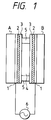
- FIG. 1 shows the general construction of a liquid crystal display device according to the present invention.
- a and B are oppositely disposed glass substrates.
- the inside surface of each of the glass substrates A and B is laminated with a transparent electrode 1, an alignment undercoat film 2, and a homeotropic-alignment film 3 that are arranged in the order named.
- a liquid crystal 4 is filled in a space defined between the homeotropic-alignment films 3, 3.
- Numerals 5 are spacers, and 6 is a power supply.
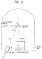
- FIG. 2 shows a thin-film deposition system or apparatus used for forming an angle-deposited film according to the present invention.
- two glass substrates A, B each coated with a transparent electrode (indium tin oxide: ITO) treated by a desired patterning were set obliquely in the apparatus, with an angle ⁇ 1 formed between the normal line on each glass-ITO substrate A, B and an evaporation source 7, and a first SiO2 film was deposited on the obliquely supported glass-ITO substrates A, B while irradiating the substrate surface with an ion beam 10 emitted from an ion gun 8.
- Conditions for a first step of ion beam assisted angle vapor deposition process were as follows. Deposition Rate: 10 ⁇ /sec.
- Ion Beam Power 500 V, 40 mA
- Ionized Gas O2 Gas Pressure: 1.5 - 3.5 x 10 ⁇ 5 Torr
- Substrate Temperature Room temperature ⁇ 1: 50 - 60 degrees SiO2 Film
- Thickness 100 - 500 ⁇
- the substrates A, B were twisted or turned in a plane of the substrates A, B over an angle of 90° (in-plane rotation), and after that they were set in an oblique position, with an angle ⁇ 2 formed between the normal line on each substrate A, B and the evaporation source 7.
- a second SiO2 film was deposited over the first SiO2 film during that time the first SiO2 film was irradiated with an ion beam 10 emitted from the ion gun 8.
- Conditions for the second step of ion beam assisted angle vapor deposition process were the same as those used in the first step of ion beam assisted vapor deposition process with the exception given below.
- Deposition Rate 2 ⁇ /sec. ⁇ 2: 75 - 85 degrees SiO2 Film Thickness: 25 - 50 ⁇
- the glass-ITO substrates A, B overcoated with an alignment undercoat film 2 of a double-layer structure were thus produced.
- the glass-ITO substrates A, B coated with the alignment undercoat film 2 were coated with a homeotropic-alignment film 3.
- a homeotropic-alignment agent (AY43-021 available from the Dow Corning Toray Silicone Co., Ltd.) composed of a silan coupling agent was coated over the alignment undercoat film 2, followed by baking at 110°C for 1 hour.
- the substrates A, B were then bonded together with spacers 5 disposed therebetween, and after that a liquid crystal (EN38 available from Chisso Corp.) was filled in a space defined between the substrates A, B and the spacers 5.
- a homeotropic-alignment liquid crystal display device or cells having a 6 ⁇ m cell thickness was produced.
- the foregoing procedure was repeated to produce eight sample cells (Sample Nos. 1 - 8) having different homeotropic-alignment undercoat film 2 sets.
- sample Nos. 9 and 10 were produced by repeating the procedure of Example 1 except that ⁇ 1 and ⁇ 2 were fixed at 60° and 85°, respectively, the two-step angle vapor deposition process was carried out without the assistance of ion beam irradiation, and the evaporation material used in the production of one sample cell (Sample No. 10) was SiO.
- sample Nos. 11 and 12 Two sample cells (Sample Nos. 11 and 12) were produced for comparative purposes by repeating the procedure of Example 1 except that ⁇ 1 and ⁇ 2 were fixed at 60° and 85°, respectively, and the in-plane rotation or twisting was omitted for one sample cell (Sample No. 11) while effected at a 180° angle for the other sample cell (Sample No. 12).
- sample cells (Sample Nos. 1 - 12) were measured for contrast ratio (CR) and ⁇ value.
- the CR is the ratio of the maximum intensity of transmitted light in the electric-field activated state to the intensity of transmitted light in the electric-field unactivated state under crossed Nicol prisms.
- the ⁇ value is the ratio of the applied voltage observed when the intensity of transmitted light becomes equal to 99% of the maximum, to the applied voltage observed when the intensity of transmitted light becomes equal to 1% of the maximum. The occurrence of alignment non-uniformity was also inspected visually. Results thus obtained are shown in Table 1.
- the in-plane rotation or twist made before the second angled vapor deposition step has no adverse effect on the CR, ⁇ and alignment non-uniformity of the cells (See Sample Nos. 11 and 12). It was found that the in-plane rotation over a 0° angle or a 180° angle successfully controlled the off-state alignment non-uniformity and temperature-induced changes in alignment direction.
- two glass substrates A, B each coated with a transparent electrode (indium tin oxide: ITO) treated by a desired patterning were set obliquely in the apparatus, with an angle ⁇ 1 formed between the normal line on each glass-ITO substrate A, B and an evaporation source 7, and an SiO2 film was deposited on the obliquely supported glass-ITO substrates A, B while irradiating the substrate surface with an ion beam 10 emitted from an ion gun 8.
- Conditions for the ion beam assisted angle vapor deposition process were as follows. Deposition Rate: 10 ⁇ /sec.
- Ion Beam Power 500 V, 40 mA
- Ionized Gas O2 Gas Pressure: 1.5 - 3.5 x 10 ⁇ 5 Torr
- Substrate Temperature Room temperature ⁇ 1: 50 - 60 degrees ⁇ a : 60 - 70 degrees
- SiO2 Film Thickness 500 ⁇
- the substrates A, B were twisted or turned in a plane of the substrates A, B over an angle of 90° and then set in an oblique position, with an angle ⁇ a formed between the normal line on each substrate A, B and the ion gun 8. Thereafter, the ion beam 10 of the same power as described above was irradiated over the SiO2 film for 2 minutes.
- the glass-ITO substrates A, B overcoated with an alignment undercoat film 2 of a single-layer structure were thus produced.
- the glass-ITO substrates A, B coated with the alignment undercoat film 2 were coated with a homeotropic-alignment film 3.
- a homeotropic-alignment agent (AY43-021 available from the Dow Corning Toray Silicone Co., Ltd.) composed of a silan coupling agent was coated over the alignment undercoat film 2, followed by baking at 110°C for 1 hour.
- the substrates A, B were then bonded together with spacers 5 disposed therebetween, and after that a liquid crystal (EN38 available from Chisso Corp.) was filled in a space defined between the substrates A, B and the spacers 5.
- a homeotropic-alignment liquid crystal display device or cell was produced. The foregoing procedure was repeated to produce five sample cells (Sample Nos. 13 - 17) having different homeotropic-alignment undercoat film 2 sets.
- sample cell (Sample No 18) was produced by repeating the procedure of Example 3 except that ⁇ 1 was fixed at 60°, and the second ion beam irradiation step was omitted.
- sample Nos. 19 and 20 Two sample cells (Sample Nos. 19 and 20) were produced for comparative purposes by repeating the procedure of Example 3 except that ⁇ 1 and ⁇ a were both fixed at 60°, and the in-plane rotation or twisting was omitted for one sample cell (Sample No. 19) while effected at a 180° angle for the other sample cell (Sample No. 20).
- sample Nos. 21 and 22 were produced by repeating the procedure of Example 1 except that ⁇ 1 and ⁇ 2 were fixed at 60° and 85°, respectively, the gas pressure was less than 2 x 10 ⁇ 5 Torr, the two-step angle vapor deposition process was carried out without the assistance of ion beam irradiation, and the evaporation material used in the production of one sample cell (Sample No. 21) was SiO.
- sample cells For purposes of performance evaluation, the sample cells (Sample Nos. 13 - 22) were measured for contrast ratio (CR) and ⁇ value. The CR and the ⁇ value are as specified above. The occurrence of alignment non-uniformity was also inspected visually. Results thus obtained are shown in Table 2. In Table 2, the marks " ⁇ ”, “ ⁇ ”, “ ⁇ ” and "X” used for evaluation of the alignment uniformity are as specified above.
- sample No. 18 It is evidenced from Table 2 that omission of the second ion beam irradiation brings about a low CR and a large ⁇ value which deteriorate the directivity of homeotropic-alignment (Sample No. 18). Excepting this No. 18, all the sample cells (Sample Nos. 13 - 17 and 19 -20) according to the present invention have contrast ratios (CR) which are considerably higher than those of the conventional cells (Sample Nos. 21 and 22). Further, excepting one sample (Sample No. 13), they are free from the alignment non-uniformity problem and have ⁇ values which are comparable to those of the conventional cells (Sample Nos. 21 and 22).
- the performance characteristics of the inventive cells are stable and not influenced very much by changes in film thickness and incident angle.
- the Sample No. 22 when compared with other Samples indicates that the ion beam assist process makes it possible to use the SiO2 as a material for forming an alignment film. As described previously, this is particular advantageous because the SiO2 has been considered as being highly chemically stable but inadequate as a material for the alignment film.
- the in-plane rotation or twist made before the second angled vapor deposition step has no adverse effect on the CR, ⁇ and alignment non-uniformity of the cells (See Sample Nos. 19 and 20). It was found that the in-plane rotation over a 0° angle or a 180° angle successfully controlled the off-state alignment non-uniformity and temperature-induced changes in alignment direction.
- a spatial light modulator (SLM) of a construction shown in FIG. 3 was produced and incorporated in an optical projection system shown in FIG. 4. Using this projection system, written images were projected as 50-times enlarged dynamic images on a screen for visual inspection of the display qualities.
- SLM spatial light modulator
- the SLM was produced in a manner described below. Using a plasma chemical vapor deposition (CVD) system, a hydrogenerated amorphous silicon (a-Si:H) layer of 15 ⁇ m thick was deposited on a glass-ITO substrate as a photoconductive layer. Then, an Si film of 2 ⁇ m was formed by vapor deposition over the photoconductive layer, thus forming a light blocking layer. On the light blocking layer were laminated five layers of alternating SiO2 and TiO2 films with ⁇ /4 unit layer thick so as to form a dielectric mirror.
- CVD plasma chemical vapor deposition
- Example A Using the thus treated substrate in combination with a glass-ITO substrate, a cell (Sample A) was produced by repeating the procedure of Example 1 and under the conditions set for producing Sample No. 3 described above.
- Example B Another cell (Sample B) was produced by repeating the procedure of Example 3 and under the conditions set for producing Sample No. 15 described above.
- sample A and Sample B were separately assembled with the optical projection system shown in FIG. 4, and the qualities of dynamic images projected on the screen were inspected visually. No non-uniformity was observed by the visual inspection at the boundary between the bright and dark areas of the dynamic images, and hence the qualities of the displayed images were quite satisfactory.
- the evaporation material may include oxides other than SiO2.
- the ionized gas may include Ar, Ar-O2 or the like.
- the present invention is not limited to reflection read-out type liquid crystal display devices but also applicable to the transmission type liquid crystal display devices. It is therefore to be understood that within the scope of the appended claims the invention may be practiced otherwise than as specifically described.
Landscapes
- Chemical & Material Sciences (AREA)
- Physics & Mathematics (AREA)
- Nonlinear Science (AREA)
- Chemical Kinetics & Catalysis (AREA)
- Engineering & Computer Science (AREA)
- Materials Engineering (AREA)
- Mechanical Engineering (AREA)
- Metallurgy (AREA)
- Organic Chemistry (AREA)
- Spectroscopy & Molecular Physics (AREA)
- Crystallography & Structural Chemistry (AREA)
- Mathematical Physics (AREA)
- General Physics & Mathematics (AREA)
- Optics & Photonics (AREA)
- Liquid Crystal (AREA)
- Physical Vapour Deposition (AREA)
- Transforming Electric Information Into Light Information (AREA)
Applications Claiming Priority (6)
| Application Number | Priority Date | Filing Date | Title |
|---|---|---|---|
| JP32102691 | 1991-11-08 | ||
| JP321026/91 | 1991-11-08 | ||
| JP32102691 | 1991-11-08 | ||
| JP28095492 | 1992-09-25 | ||
| JP280954/92 | 1992-09-25 | ||
| JP04280954A JP3132193B2 (ja) | 1991-11-08 | 1992-09-25 | 液晶表示デバイス及び液晶表示デバイスの製造方法 |
Publications (2)
| Publication Number | Publication Date |
|---|---|
| EP0541388A1 true EP0541388A1 (fr) | 1993-05-12 |
| EP0541388B1 EP0541388B1 (fr) | 2000-01-26 |
Family
ID=26553995
Family Applications (1)
| Application Number | Title | Priority Date | Filing Date |
|---|---|---|---|
| EP92310185A Expired - Lifetime EP0541388B1 (fr) | 1991-11-08 | 1992-11-06 | Procédé de fabrication d'un dispositif d'affichage à crystal liquide |
Country Status (4)
| Country | Link |
|---|---|
| US (1) | US5268781A (fr) |
| EP (1) | EP0541388B1 (fr) |
| JP (1) | JP3132193B2 (fr) |
| DE (1) | DE69230608T2 (fr) |
Cited By (6)
| Publication number | Priority date | Publication date | Assignee | Title |
|---|---|---|---|---|
| EP0712024A3 (fr) * | 1994-11-08 | 1997-06-04 | Seiko Instr Inc | Procédé pour introduire une orientation homéotrope légèrement inclinée dans un cristal liquide, et valve de lumière à cristal liquide électro-optique |
| US6103318A (en) * | 1997-06-06 | 2000-08-15 | Corning Incorporated | Method for making an optical waveguide component using a low-stress silicon photomask |
| EP1513004A1 (fr) * | 2003-09-02 | 2005-03-09 | Sony Corporation | Dispositif d'affichage réflectif à cristal liquide, son procédé de fabrication et une unité d'un dispositif d'affichage à cristal liquide |
| EP1515182A3 (fr) * | 2003-09-11 | 2005-03-23 | Sony Corporation | Dispositif d'affichage à cristaux liquides du type réflectif et son procédé de sa fabrication |
| EP1541661A1 (fr) * | 2003-12-11 | 2005-06-15 | Sony International (Europe) GmbH | Composé comprenant un matériau liquide cristalline et un additif |
| WO2008108477A1 (fr) * | 2007-03-02 | 2008-09-12 | Canon Kabushiki Kaisha | Procédé de formation de couche et processus de fabrication de dispositif d'affichage à cristaux liquides |
Families Citing this family (52)
| Publication number | Priority date | Publication date | Assignee | Title |
|---|---|---|---|---|
| US6346975B2 (en) | 1998-08-04 | 2002-02-12 | International Business Machines Corporation | Liquid crystal display having alignment layer using ion bombarded amorphous material 100Å thickness or less |
| JP2000056297A (ja) | 1998-08-07 | 2000-02-25 | Victor Co Of Japan Ltd | 液晶表示デバイス |
| US6519018B1 (en) | 1998-11-03 | 2003-02-11 | International Business Machines Corporation | Vertically aligned liquid crystal displays and methods for their production |
| US6426786B1 (en) | 1999-06-01 | 2002-07-30 | International Business Machines Corporation | Method of homeotropic alignment or tilted homeotropic alignment of liquid crystals by single oblique evaporation of oxides and liquid crystal display device formed thereby |
| US6313896B1 (en) * | 1999-08-31 | 2001-11-06 | International Business Machines Corporation | Method for forming a multi-domain alignment layer for a liquid crystal display device |
| US6724449B1 (en) * | 2000-03-27 | 2004-04-20 | International Business Machines Corporation | Vertical aligned liquid crystal display and method using dry deposited alignment layer films |
| US6632483B1 (en) * | 2000-06-30 | 2003-10-14 | International Business Machines Corporation | Ion gun deposition and alignment for liquid-crystal applications |
| JP3510845B2 (ja) | 2000-08-29 | 2004-03-29 | Hoya株式会社 | 反射防止膜を有する光学部材 |
| AU756842B2 (en) | 2000-08-29 | 2003-01-23 | Hoya Corporation | Optical element having antireflection film |
| US6791648B2 (en) * | 2001-03-15 | 2004-09-14 | Seiko Epson Corporation | Liquid crystal device, projection display device and, manufacturing method for substrate for liquid crystal device |
| CN1267777C (zh) * | 2001-06-26 | 2006-08-02 | 索尼公司 | 反射液晶显示装置、显示设备、投影光学系统和投影显示系统 |
| JP2004045784A (ja) * | 2002-07-12 | 2004-02-12 | Sony Corp | 液晶パネルおよびその製造方法 |
| US20040156004A1 (en) * | 2002-10-23 | 2004-08-12 | Jvc (Victor Company Of Japan, Ltd.) | Liquid crystal display element and method of forming alignment layer of the liquid crystal element |
| JP3767589B2 (ja) * | 2003-09-04 | 2006-04-19 | セイコーエプソン株式会社 | 無機配向膜の形成方法、無機配向膜、電子デバイス用基板、液晶パネルおよび電子機器 |
| JP2005173544A (ja) * | 2003-11-19 | 2005-06-30 | Seiko Epson Corp | 液晶装置及び電子機器 |
| JP4556426B2 (ja) * | 2003-12-22 | 2010-10-06 | ソニー株式会社 | 液晶表示装置および液晶表示装置の製造方法 |
| US20050238801A1 (en) * | 2004-04-27 | 2005-10-27 | Chia-Te Lin | Method for fabricating an alignment layer for liquid crystal applications |
| KR100628271B1 (ko) * | 2004-05-24 | 2006-09-27 | 엘지.필립스 엘시디 주식회사 | 이온빔 조사를 이용한 배향법 |
| JP2006119401A (ja) * | 2004-10-22 | 2006-05-11 | Seiko Epson Corp | 電気光学装置の製造方法及び製造装置、電気光学装置並びに電子機器 |
| JP4670452B2 (ja) | 2005-04-19 | 2011-04-13 | セイコーエプソン株式会社 | 液晶パネルの製造方法 |
| US20060256267A1 (en) * | 2005-05-10 | 2006-11-16 | Bone Matthew F | Method for manufacturing liquid crystal display devices and devices manufactured thereby |
| JP4544048B2 (ja) | 2005-06-20 | 2010-09-15 | セイコーエプソン株式会社 | 液晶パネルおよび電子機器 |
| JP2007108371A (ja) | 2005-10-13 | 2007-04-26 | Seiko Epson Corp | 液晶パネル、液晶パネルの製造方法および電子機器 |
| US20070218213A1 (en) * | 2006-03-14 | 2007-09-20 | Chih-Chien Chou | Method of manufacturing liquid crystal alignment film |
| JP2007286468A (ja) * | 2006-04-19 | 2007-11-01 | Seiko Epson Corp | 液晶装置の製造方法 |
| JP4789704B2 (ja) * | 2006-06-07 | 2011-10-12 | シチズンファインテックミヨタ株式会社 | 液晶パネルの製造方法 |
| JP4702198B2 (ja) * | 2006-06-27 | 2011-06-15 | セイコーエプソン株式会社 | 配向膜、配向膜の形成方法、電子デバイス用基板、液晶パネルおよび電子機器 |
| JP4846603B2 (ja) * | 2007-01-11 | 2011-12-28 | 株式会社アルバック | 配向膜の製造方法 |
| JP2008191264A (ja) * | 2007-02-01 | 2008-08-21 | Seiko Epson Corp | 液晶装置、配向膜の製造方法、液晶装置の製造方法 |
| US7803229B2 (en) * | 2007-02-15 | 2010-09-28 | Himax Display, Inc. | Apparatus and method for compensating uniformity of film thickness |
| FR2917510B1 (fr) | 2007-06-13 | 2012-01-27 | Essilor Int | Article d'optique revetu d'un revetement antireflet comprenant une sous-couche partiellement formee sous assistance ionique et procede de fabrication |
| JP2010033015A (ja) * | 2008-06-30 | 2010-02-12 | Canon Inc | 無機配向膜の製造方法及び無機配向膜 |
| US8102491B2 (en) * | 2008-07-10 | 2012-01-24 | Canon Kabushiki Kaisha | Liquid crystal apparatus and method of producing the same |
| FR2943798B1 (fr) | 2009-03-27 | 2011-05-27 | Essilor Int | Article d'optique revetu d'un revetement antireflet ou reflechissant comprenant une couche electriquement conductrice a base d'oxyde d'etain et procede de fabrication |
| JP5515631B2 (ja) * | 2009-10-30 | 2014-06-11 | 株式会社Jvcケンウッド | 液晶表示装置及びその製造方法 |
| JP2016191847A (ja) * | 2015-03-31 | 2016-11-10 | セイコーエプソン株式会社 | 液晶装置の製造方法、液晶装置、及び電子機器 |
| EP3392680A1 (fr) | 2017-04-18 | 2018-10-24 | Essilor International | Article optique présentant un revêtement interférentiel résistant à l'abrasion et à la température ayant un rapport d'épaisseur optimisé des couches à indice de réfraction faible et élevé |
| EP3640688B1 (fr) | 2018-10-18 | 2022-10-05 | Essilor International | Article optique comportant un revêtement interférentiel ayant une meilleure résistance à l'abrasion |
| EP3640687B1 (fr) | 2018-10-18 | 2024-12-04 | Essilor International | Article optique comportant un revêtement interférentiel avec une haute résistance à l'abrasion |
| PL3654071T3 (pl) | 2018-11-19 | 2025-01-07 | Essilor International | Soczewka optyczna mająca powłokę interferencyjną i wielowarstwowy system poprawiający odporność na ścieranie |
| EP3654072B1 (fr) | 2018-11-19 | 2024-09-04 | Essilor International | Lentille optique doté d'un revêtement interférentiel de filtrage et système multicouche pour améliorer la résistance à l'abrasion |
| EP3884314B1 (fr) | 2018-11-19 | 2024-01-03 | Essilor International | Lentille optique ayant un revêtement de miroir et un système multicouche pour améliorer la résistance à l'abrasion |
| WO2020104388A2 (fr) | 2018-11-19 | 2020-05-28 | Essilor International | Lentille optique à revêtement interférentiel amélioré et système multicouche pour améliorer la résistance à l'abrasion |
| CN113227848B (zh) | 2018-12-18 | 2023-04-18 | 依视路国际公司 | 具有反射涂层的高耐磨性光学制品 |
| EP4095570A1 (fr) | 2021-05-27 | 2022-11-30 | Essilor International | Lentille optique dotée d'un miroir asymétrique |
| EP4102264A1 (fr) | 2021-06-09 | 2022-12-14 | Essilor International | Lentille optique dotée d'un revêtement antireflet réfléchissant la lumière bleue nocive et le rayonnement infrarouge proche |
| WO2022258793A1 (fr) | 2021-06-09 | 2022-12-15 | Essilor International | Lentille optique ayant un revêtement antireflet réfléchissant la lumière bleue |
| EP4102265A1 (fr) | 2021-06-09 | 2022-12-14 | Essilor International | Lentille optique comportant un revêtement antireflet réfléchissant la lumière bleue nocive |
| EP4109141A1 (fr) | 2021-06-21 | 2022-12-28 | Essilor International | Lentille optique comportant un revêtement interférentiel absorbant la lumière |
| BR112023025530A2 (pt) | 2021-06-21 | 2024-02-27 | Essilor Int | Lente óptica tendo um revestimento interferencial e um sistema multicamada para melhoramento da resistência à abrasão |
| US20260086394A1 (en) | 2022-04-26 | 2026-03-26 | Essilor International | Photochromic optical article having a mirror coating |
| EP4535045A1 (fr) | 2023-10-02 | 2025-04-09 | Essilor International | Lentille optique ayant un revêtement antireflet à bande étroite reflétant la lumière bleue |
Citations (1)
| Publication number | Priority date | Publication date | Assignee | Title |
|---|---|---|---|---|
| FR2413735A1 (fr) * | 1977-12-28 | 1979-07-27 | Ebauches Sa | Procede de fabrication d'une cellule d'affichage electro-optique passif a cristal liquide nematique en helice et cellule d'affichage electro-optique passif obtenue par la mise en oeuvre de ce procede |
Family Cites Families (11)
| Publication number | Priority date | Publication date | Assignee | Title |
|---|---|---|---|---|
| US4153529A (en) * | 1975-04-21 | 1979-05-08 | Hughes Aircraft Company | Means and method for inducing uniform parallel alignment of liquid crystal material in a liquid crystal cell |
| AT382251B (de) * | 1977-04-20 | 1987-02-10 | Citizen Watch Co Ltd | Verfahren und vorrichtung zum herstellen einer orientierungsschicht fuer fluessigkristallanzeigezellen |
| JPS5843532B2 (ja) * | 1978-07-13 | 1983-09-27 | 鹿島建設株式会社 | ケ−ソンの沈設工法 |
| JPS5619030A (en) * | 1979-07-25 | 1981-02-23 | Sharp Corp | Production of liquid crystal display element |
| JPS5683718A (en) * | 1979-12-13 | 1981-07-08 | Asahi Glass Co Ltd | Liquid crystal display element |
| JPS56137330A (en) * | 1980-03-29 | 1981-10-27 | Koki Hiroshima | Orientation treatment of liquid crystal cell substrate |
| JPS56155923A (en) * | 1980-05-06 | 1981-12-02 | Seiko Epson Corp | Liquid crystal display device |
| JPS5754919A (en) * | 1980-09-19 | 1982-04-01 | Toshiba Corp | Liquid crystal element |
| DE3424530A1 (de) * | 1984-03-02 | 1985-09-05 | BBC Aktiengesellschaft Brown, Boveri & Cie., Baden, Aargau | Verfahren zur herstellung einer orientierungsschicht auf einer ebenen oberflaeche einer platte und vorrichtung zur durchfuehrung des verfahrens |
| US4776674A (en) * | 1986-06-25 | 1988-10-11 | American Telephone And Telegraph Company, At&T Bell Laboratories | Liquid crystal device with chemically-induced high-tilt alignment coating |
| US4897290A (en) * | 1986-09-26 | 1990-01-30 | Konishiroku Photo Industry Co., Ltd. | Method for manufacturing the substrate for liquid crystal display |
-
1992
- 1992-09-25 JP JP04280954A patent/JP3132193B2/ja not_active Expired - Lifetime
- 1992-11-06 EP EP92310185A patent/EP0541388B1/fr not_active Expired - Lifetime
- 1992-11-06 US US07/972,521 patent/US5268781A/en not_active Expired - Lifetime
- 1992-11-06 DE DE69230608T patent/DE69230608T2/de not_active Expired - Lifetime
Patent Citations (1)
| Publication number | Priority date | Publication date | Assignee | Title |
|---|---|---|---|---|
| FR2413735A1 (fr) * | 1977-12-28 | 1979-07-27 | Ebauches Sa | Procede de fabrication d'une cellule d'affichage electro-optique passif a cristal liquide nematique en helice et cellule d'affichage electro-optique passif obtenue par la mise en oeuvre de ce procede |
Non-Patent Citations (1)
| Title |
|---|
| PATENT ABSTRACTS OF JAPAN vol. 5, no. 69 (P-60)23 February 1981 & JP-A-56 019 030 ( SHARP CORP. ) 9 May 1981 * |
Cited By (11)
| Publication number | Priority date | Publication date | Assignee | Title |
|---|---|---|---|---|
| EP0712024A3 (fr) * | 1994-11-08 | 1997-06-04 | Seiko Instr Inc | Procédé pour introduire une orientation homéotrope légèrement inclinée dans un cristal liquide, et valve de lumière à cristal liquide électro-optique |
| US5745205A (en) * | 1994-11-08 | 1998-04-28 | Seiko Instruments Inc. | Method of introducing slightly titlting homeotropic orientation into liquid crystal, liquid crystal electro-optical device, and liquid crystal light valve |
| US6103318A (en) * | 1997-06-06 | 2000-08-15 | Corning Incorporated | Method for making an optical waveguide component using a low-stress silicon photomask |
| EP1513004A1 (fr) * | 2003-09-02 | 2005-03-09 | Sony Corporation | Dispositif d'affichage réflectif à cristal liquide, son procédé de fabrication et une unité d'un dispositif d'affichage à cristal liquide |
| US7193671B2 (en) | 2003-09-02 | 2007-03-20 | Sony Corporation | Reflective liquid crystal display device having obliquely evaporated alignment film on vertically evaporated film, method of manufacturing the same, and vertically aligned liquid crystal display unit |
| EP1515182A3 (fr) * | 2003-09-11 | 2005-03-23 | Sony Corporation | Dispositif d'affichage à cristaux liquides du type réflectif et son procédé de sa fabrication |
| US7227604B2 (en) | 2003-09-11 | 2007-06-05 | Sony Corporation | Reflective liquid crystal display device having first and second obliquely evaporated alignment films, for preventing burn-in |
| EP1541661A1 (fr) * | 2003-12-11 | 2005-06-15 | Sony International (Europe) GmbH | Composé comprenant un matériau liquide cristalline et un additif |
| WO2005059061A1 (fr) * | 2003-12-11 | 2005-06-30 | Sony Deutschland Gmbh | Composition comprenant une matiere a cristal liquide et un additif |
| US7758772B2 (en) | 2003-12-11 | 2010-07-20 | Sony Deutschland Gmbh | Composition comprising a liquid crystal material and an additive |
| WO2008108477A1 (fr) * | 2007-03-02 | 2008-09-12 | Canon Kabushiki Kaisha | Procédé de formation de couche et processus de fabrication de dispositif d'affichage à cristaux liquides |
Also Published As
| Publication number | Publication date |
|---|---|
| JPH05203958A (ja) | 1993-08-13 |
| DE69230608D1 (de) | 2000-03-02 |
| US5268781A (en) | 1993-12-07 |
| DE69230608T2 (de) | 2000-09-21 |
| JP3132193B2 (ja) | 2001-02-05 |
| EP0541388B1 (fr) | 2000-01-26 |
Similar Documents
| Publication | Publication Date | Title |
|---|---|---|
| EP0541388B1 (fr) | Procédé de fabrication d'un dispositif d'affichage à crystal liquide | |
| US6426786B1 (en) | Method of homeotropic alignment or tilted homeotropic alignment of liquid crystals by single oblique evaporation of oxides and liquid crystal display device formed thereby | |
| WO1996010773A1 (fr) | Dispositif de compensation comprenant un film mineral mince pour ameliorer l'echelle des gris dans les affichages a cristaux liquides a structure nematique torsadee | |
| US6346975B2 (en) | Liquid crystal display having alignment layer using ion bombarded amorphous material 100Å thickness or less | |
| EP0412843B1 (fr) | Dispositif d'affichage à cristal liquide adressé optiquement | |
| JP2792700B2 (ja) | 正の誘電体異方性液晶及び著しく傾斜した非垂直表面配列を伴う光バルブと、それに関する操作方法 | |
| WO1996010770A1 (fr) | Compensateur a plaque o en polymere organique destine a ameliorer la performance de l'echelle de gris dans des afficheurs a cristaux liquides nematiques en helice | |
| US6816219B2 (en) | Liquid crystal panel and method for manufacturing same | |
| US6163353A (en) | Method for fabricating a reflective liquid crystal display panel having a reflector with an inclined surface and devices made | |
| US5013139A (en) | Alignment layer for liquid crystal devices and method of forming | |
| US7372524B2 (en) | Liquid crystal display device | |
| KR100493351B1 (ko) | 액정 디바이스 | |
| EP1507163A2 (fr) | Affichage à cristaux liquides | |
| JP2003050397A (ja) | 配向膜を備えた基板とその製造方法 | |
| US6882391B2 (en) | Method of forming a multi-domain HTN mode liquid crystal display device | |
| JP3271384B2 (ja) | 位相制御素子用の液晶配向膜の形成方法 | |
| US5790221A (en) | Method of manufacturing a liquid crystal cell | |
| KR0141909B1 (ko) | 액정 표시 디바이스 제조 방법 | |
| KR0151949B1 (ko) | 액정 표시 디바이스 | |
| JP2791345B2 (ja) | 強誘電性液晶パネル | |
| JPH1096894A (ja) | 液晶の表示、スイッチあるいは画像処理の装置 | |
| JPH10161127A (ja) | 垂直配向型の液晶表示デバイス | |
| JP3073657B2 (ja) | 液晶ライトバルブ及びそれを用いた投射型液晶表示装置 | |
| US5521730A (en) | Photoconductive-type liquid crystal light valve with a shielding layer made of manganese oxide and silicon dioxide | |
| JP2761253B2 (ja) | 光書込み形液晶表示装置 |
Legal Events
| Date | Code | Title | Description |
|---|---|---|---|
| PUAI | Public reference made under article 153(3) epc to a published international application that has entered the european phase |
Free format text: ORIGINAL CODE: 0009012 |
|
| AK | Designated contracting states |
Kind code of ref document: A1 Designated state(s): DE FR GB |
|
| 17P | Request for examination filed |
Effective date: 19930623 |
|
| 17Q | First examination report despatched |
Effective date: 19950328 |
|
| GRAG | Despatch of communication of intention to grant |
Free format text: ORIGINAL CODE: EPIDOS AGRA |
|
| GRAG | Despatch of communication of intention to grant |
Free format text: ORIGINAL CODE: EPIDOS AGRA |
|
| GRAH | Despatch of communication of intention to grant a patent |
Free format text: ORIGINAL CODE: EPIDOS IGRA |
|
| GRAH | Despatch of communication of intention to grant a patent |
Free format text: ORIGINAL CODE: EPIDOS IGRA |
|
| GRAA | (expected) grant |
Free format text: ORIGINAL CODE: 0009210 |
|
| AK | Designated contracting states |
Kind code of ref document: B1 Designated state(s): DE FR GB |
|
| ET | Fr: translation filed | ||
| REF | Corresponds to: |
Ref document number: 69230608 Country of ref document: DE Date of ref document: 20000302 |
|
| PLBE | No opposition filed within time limit |
Free format text: ORIGINAL CODE: 0009261 |
|
| 26N | No opposition filed | ||
| REG | Reference to a national code |
Ref country code: GB Ref legal event code: IF02 |
|
| PGFP | Annual fee paid to national office [announced via postgrant information from national office to epo] |
Ref country code: DE Payment date: 20101104 Year of fee payment: 19 |
|
| PGFP | Annual fee paid to national office [announced via postgrant information from national office to epo] |
Ref country code: GB Payment date: 20101103 Year of fee payment: 19 |
|
| PGFP | Annual fee paid to national office [announced via postgrant information from national office to epo] |
Ref country code: FR Payment date: 20111118 Year of fee payment: 20 |
|
| REG | Reference to a national code |
Ref country code: DE Ref legal event code: R082 Ref document number: 69230608 Country of ref document: DE Representative=s name: MANITZ, FINSTERWALD & PARTNER GBR, DE |
|
| REG | Reference to a national code |
Ref country code: DE Ref legal event code: R082 Ref document number: 69230608 Country of ref document: DE Representative=s name: MANITZ FINSTERWALD PATENTANWAELTE PARTMBB, DE Effective date: 20120430 Ref country code: DE Ref legal event code: R082 Ref document number: 69230608 Country of ref document: DE Representative=s name: MANITZ, FINSTERWALD & PARTNER GBR, DE Effective date: 20120430 Ref country code: DE Ref legal event code: R081 Ref document number: 69230608 Country of ref document: DE Owner name: JVC KENWOOD CORPORATION, YOKOHAMA-SHI, JP Free format text: FORMER OWNER: VICTOR COMPANY OF JAPAN, LTD., YOKOHAMA, KANAGAWA, JP Effective date: 20120430 Ref country code: DE Ref legal event code: R081 Ref document number: 69230608 Country of ref document: DE Owner name: JVC KENWOOD CORPORATION, JP Free format text: FORMER OWNER: VICTOR COMPANY OF JAPAN, LTD., YOKOHAMA, JP Effective date: 20120430 |
|
| REG | Reference to a national code |
Ref country code: FR Ref legal event code: TP Owner name: JVC KENWOOD CORPORATION, JP Effective date: 20120705 |
|
| REG | Reference to a national code |
Ref country code: DE Ref legal event code: R071 Ref document number: 69230608 Country of ref document: DE |
|
| REG | Reference to a national code |
Ref country code: DE Ref legal event code: R071 Ref document number: 69230608 Country of ref document: DE |
|
| REG | Reference to a national code |
Ref country code: GB Ref legal event code: PE20 Expiry date: 20121105 |
|
| PG25 | Lapsed in a contracting state [announced via postgrant information from national office to epo] |
Ref country code: GB Free format text: LAPSE BECAUSE OF EXPIRATION OF PROTECTION Effective date: 20121105 |