EP0541455A1 - Verfahren zur Wandlung von Impedanzverhältnissen, anwendbar insbesondere für industrielle Druckgeber - Google Patents
Verfahren zur Wandlung von Impedanzverhältnissen, anwendbar insbesondere für industrielle Druckgeber Download PDFInfo
- Publication number
- EP0541455A1 EP0541455A1 EP92420367A EP92420367A EP0541455A1 EP 0541455 A1 EP0541455 A1 EP 0541455A1 EP 92420367 A EP92420367 A EP 92420367A EP 92420367 A EP92420367 A EP 92420367A EP 0541455 A1 EP0541455 A1 EP 0541455A1
- Authority
- EP
- European Patent Office
- Prior art keywords
- output
- input
- voltage
- switch
- signal
- Prior art date
- Legal status (The legal status is an assumption and is not a legal conclusion. Google has not performed a legal analysis and makes no representation as to the accuracy of the status listed.)
- Granted
Links
Images


Classifications
-
- G—PHYSICS
- G01—MEASURING; TESTING
- G01R—MEASURING ELECTRIC VARIABLES; MEASURING MAGNETIC VARIABLES
- G01R27/00—Arrangements for measuring resistance, reactance, impedance, or electric characteristics derived therefrom
- G01R27/02—Measuring real or complex resistance, reactance, impedance, or other two-pole characteristics derived therefrom, e.g. time constant
- G01R27/26—Measuring inductance or capacitance; Measuring quality factor, e.g. by using the resonance method; Measuring loss factor; Measuring dielectric constants ; Measuring impedance or related variables
-
- G—PHYSICS
- G01—MEASURING; TESTING
- G01L—MEASURING FORCE, STRESS, TORQUE, WORK, MECHANICAL POWER, MECHANICAL EFFICIENCY, OR FLUID PRESSURE
- G01L9/00—Measuring steady of quasi-steady pressure of fluid or fluent solid material by electric or magnetic pressure-sensitive elements; Transmitting or indicating the displacement of mechanical pressure-sensitive elements, used to measure the steady or quasi-steady pressure of a fluid or fluent solid material, by electric or magnetic means
- G01L9/12—Measuring steady of quasi-steady pressure of fluid or fluent solid material by electric or magnetic pressure-sensitive elements; Transmitting or indicating the displacement of mechanical pressure-sensitive elements, used to measure the steady or quasi-steady pressure of a fluid or fluent solid material, by electric or magnetic means by making use of variations in capacitance, i.e. electric circuits therefor
-
- H—ELECTRICITY
- H03—ELECTRONIC CIRCUITRY
- H03M—CODING; DECODING; CODE CONVERSION IN GENERAL
- H03M1/00—Analogue/digital conversion; Digital/analogue conversion
- H03M1/66—Digital/analogue converters
- H03M1/82—Digital/analogue converters with intermediate conversion to time interval
- H03M1/822—Digital/analogue converters with intermediate conversion to time interval using pulse width modulation
Definitions
- the present invention is in the field of electronics, and it relates to measurement methods and their means of implementation, in particular a converter of impedance reports with digital or analog output, as well as their applications in a transmitter of industrial pressure.
- the present invention thus aims to provide means, methods and devices, aimed at optimizing the reliability and precision of the measurement cells, in particular the capacitive pressure measurement cells working in hostile industrial environments, to allow a control thereof. more precise and more automated and, at equal performance, lower the cost of equipment.
- a subsequent step consists in applying the output E of the synchronous detector to the input of an analog integrator whose output provides the voltage Vm which is used for the measurement and which is used to generate V1 (t) and V2 (t) at the second input of the impedances, from which it follows that, the coupling of the inputs and outputs of the voltages being thus achieved, the voltage Vm generated by the loop formed by the preceding elements converges to a state of equilibrium and therefore provides a value of the ratio Z1 / Z1 + Z2 depending only on the voltages Vr and V0, to the exclusion of any other electrical quantity in the circuit.
- a subsequent step consists in applying the output of the synchronous detector to the input of an analog / digital converter of integrator type in the mathematical sense, the output of which constitutes the digital representation of the output of the synchronous detector. , usable for data processing (calculation of Vm / Vr and Z1 / Z1 + Z2), then to convert with a digital-analog converter this digital representation into the voltage Vm which is applied to the second input of the impedances.
- the second object of the invention is also a digital / analog conversion method, in particular applicable as an improvement to the aforementioned methods, but also in any other situation where such a conversion is necessary, this method constituting an invention in itself.
- fractional duty cycle converter a digital value is applied to the input of a duty cycle converter of period T ′ fractionated into at least two fractions constituting as much "subwords" of at least one bit each; it will be noted that the fractional duty cycle converter replaces, in the present method, and according to a fourth variant, the abovementioned analog converter.
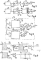
- a device for measuring the ratio of two impedances Z1 and Z2, also known as the impedance ratio converter, is distributed over two main blocks 1a and 1c , the block 1a designating a measurement cell, such for example as a capacitive pressure measurement cell, while block 1c designates the functional part of the measurement device without the reading or recording devices for the measurements.
- the whole converter is controlled by a logic signal Vh generated by a low frequency clock 2, of the order of 500 Hz.
- Vh generated by a low frequency clock 2
- Vr, Vm, ground and a switching assembly 1f two square signals are generated V1 (t) and V2 (t) whose algebraic amplitude is a function of these voltages.
- the switching assembly of the sub-block 1f in FIG. 1 comprises two switches 4,6, of the MOSFET type for example, each provided with two inputs and one output, each of said inputs being able to be related to the respective output under the impulse of the clock voltage Vh, an input, called first, of the first switch 4 being connected to the voltage source Vr, an input, called first of the second switch 6 being connected at the zero voltage source (ground) Vo, the inputs, called seconds, of said switches being connected together to receive said voltage Vm, while the output of the first switch 4 is connected to the input of impedance Z1, and the output 5 of the second switch 6 is connected to the input of the impedance Z2, the outputs of the impedances Z1 and Z2 being connected to an output line 7.
- the signals V1 (t) and V2 (t) are sent in a bridge with two branches formed by the impedances to be measured Z1 and Z2; the impedance output line 7, forming the midpoint of this bridge, is connected to the inverting input 10 of an operational amplifier 12 wired according to a "trans-impedance" type configuration, the looping impedance Zm of which is of the same nature as Z1 and Z2; it follows from this arrangement that the output of the amplifier 12 is constituted by a square signal V (t), called an error signal, the algebraic amplitude E of which represents the imbalance of the bridge.
- the signal V (t) (output 14 of the amplifier 12) is applied to the input 16 of a synchronous demodulator (or detector) 18 controlled (20) by the clock 2, which demodulator extracts the error signal E which will be used to form the voltage Vm.
- the error signal E is then applied to the input of an integrator 24 whose output provides the voltage Vm which, at the same time, can be used for measurement and is used to generate V1 (t) and V2 (t) at the second input of the impedances Z1, Z2, which ensures convergence of the loop towards an equilibrium state.
- V1 / Z1 + V2 / Z2 0 in which: V1 and V2 are the algebraic amplitudes of V1 (t) and V2 (t), and Z1 and Z2 the (complex) impedances of the bridge.
- V1C1 + V2C2 0
- V1 and V2 depends on the wiring of the switches of the switching assembly and it is thus possible to select the ratio to be measured, depending on the nature of the application.
- transimpedance assembly allows the introduction of an additional gain in the loop and, provided that the criterion of stability of the loop is met, makes it possible to reduce to a negligible level the physical imperfections of the components of the loop (for example : voltage and offset currents of operational amplifiers); this gain can be obtained by adjusting the value of Zm.
- the lines connecting said capacitors on the one hand to the inputs of said electronic switches 4 and 6, and at the inverting input of said operational amplifier 12, are so-called coaxial lines whose shields 3 ′, 5′ and 7 ′ are connected to the mass ; this is expressed by the presence of the sub-block 1d and the absence of the sub-block 1e .
- the lines connecting said capacities on the one hand at the inputs of said electronic switches 4,6 and at the inverting input of said operational amplifier 12, are also coaxial lines, the shields 3 ′, 5 ′ lines connecting said capacities to said switches being connected to ground, while the shield 7 ′ of line 7 connecting said capacities to said operational amplifier is connected to the inverting input and to the output of a second operational amplifier 13 mounted as a follower amplifier to achieve "active guard"; this is expressed by the absence of sub-block 1d and the presence of sub-block 1e .
- the output signal E 22 of the synchronous detector 18 is applied to the input of a converter analog-digital (A / D) 30 of the integrator type whose output 32 is directed on the one hand to data processing 33, and on the other hand to a digital analog converter (D / A) 34 whose analog output 35, which constitutes Vm, is looped back, via the switching assembly 1f , to the impedances Z1, Z2.
- a / D converter analog-digital
- D / A digital analog converter
- the error signal E is applied as the control voltage at the input of an oscillator, or voltage-frequency converter V / F, 36 incorporating means for, depending on the sign of the applied voltage, send pulses to one or other of the two outputs 37, 38 respectively on the counting input or the countdown input of a binary up-down counter 40 with outputs parallels 42 providing a binary "word" M and fulfilling the function of integrator; the word M is directed on the one hand to a data processing 43, and on the other hand to a digital-analog converter 44 whose output represents Vm.
- such CNARCF converter includes functionally: two digital-duty cycle converters 51 and 52, an analog switch 54 with logic control with two inputs and one output, a time base 59 of period T ′ common to the two converters and also controlling the switch 54, and two low-pass filters 53 and 58, called first and second respectively.
- the output of the first converter 51 is connected to the first input 55 of the switch 54, and the output of the second converter 52 is connected to the second input 56 of the switch through said second low-pass filter 58; the output 57 Vs (t) of the switch 54 is itself connected to the input of the first low-pass filter 53.
- an operational amplifier 63 (12), a converter V / F 66 (36) receiving the output voltage of a synchronous detector 69 (22) and supplying counting 65 (37) and down counting 65 ′ (38) pulses to an up-down counter 68 (40) at sixteen bits whose parallel output 70 (42) is addressed on the one hand to a CNARCF 64 (50), and on the other hand to a parallel-serial converter P / S 72 whose output 74 is connected to a "serial link" 76 for an external microprocessor for controlling the CNARCF, a S / P serial-parallel converter 78, and an EEPROM memory 79 intended for the storage of certain coefficients specific to the measurement cell or to the conversion electronics.
- a decoder 80 under the dependence of a S / P serial-parallel converter 78, controls the operations of the switching matrix 62.
Landscapes
- Physics & Mathematics (AREA)
- General Physics & Mathematics (AREA)
- Engineering & Computer Science (AREA)
- Theoretical Computer Science (AREA)
- Measurement Of Resistance Or Impedance (AREA)
- Analogue/Digital Conversion (AREA)
Applications Claiming Priority (2)
| Application Number | Priority Date | Filing Date | Title |
|---|---|---|---|
| FR9113160 | 1991-10-21 | ||
| FR9113160A FR2682768A1 (fr) | 1991-10-21 | 1991-10-21 | Methodes de conversion de rapports d'impedances applicables aux appareils de mesure, notamment aux transmetteurs de pression industriels, et leurs dispositifs de mise en óoeuvre. |
Publications (2)
| Publication Number | Publication Date |
|---|---|
| EP0541455A1 true EP0541455A1 (de) | 1993-05-12 |
| EP0541455B1 EP0541455B1 (de) | 1997-09-03 |
Family
ID=9418294
Family Applications (1)
| Application Number | Title | Priority Date | Filing Date |
|---|---|---|---|
| EP19920420367 Expired - Lifetime EP0541455B1 (de) | 1991-10-21 | 1992-10-21 | Verfahren zur Wandlung von Impedanzverhältnissen, anwendbar insbesondere für industrielle Druckgeber |
Country Status (3)
| Country | Link |
|---|---|
| EP (1) | EP0541455B1 (de) |
| DE (1) | DE69221989T2 (de) |
| FR (1) | FR2682768A1 (de) |
Cited By (2)
| Publication number | Priority date | Publication date | Assignee | Title |
|---|---|---|---|---|
| EP0600148A1 (de) * | 1992-11-04 | 1994-06-08 | VEGA Grieshaber GmbH & Co. | Verfahren und Anordnung zur Kapazitätsmessung |
| CN109683538A (zh) * | 2019-02-22 | 2019-04-26 | 无锡昆仑富士仪表有限公司 | 一种功能安全压力变送器 |
Families Citing this family (1)
| Publication number | Priority date | Publication date | Assignee | Title |
|---|---|---|---|---|
| DE102018121463A1 (de) * | 2018-09-03 | 2020-03-05 | Ifm Electronic Gmbh | Kapazitiver Drucksensor mit einer Druckmesszelle und einer Auswerteeinheit, die räumlich getrennt voneinander angeordnet sind |
Citations (7)
| Publication number | Priority date | Publication date | Assignee | Title |
|---|---|---|---|---|
| FR2316798A1 (fr) * | 1975-07-02 | 1977-01-28 | Bendix Corp | Systeme perfectionne de conversion capacite/numerique |
| EP0121841A2 (de) * | 1983-04-07 | 1984-10-17 | Siemens Aktiengesellschaft | Verfahren zur Erhöhung der Zeitauflösung in digitalen Systemen |
| EP0159786A1 (de) * | 1984-03-09 | 1985-10-30 | Automatic Systems Laboratories Limited | Messung von Impedanzverhältnissen |
| GB2177806A (en) * | 1985-07-09 | 1987-01-28 | Thomson Csf | Measuring capacity ratios |
| WO1987006711A1 (en) * | 1986-04-23 | 1987-11-05 | Rosemount Inc. | Measurement circuit |
| EP0421395A2 (de) * | 1989-10-06 | 1991-04-10 | Endress u. Hauser GmbH u. Co. | Anordnung zur Umwandlung einer elektrischen Eingangsgrösse in ein dazu proportionales elektrisches Gleichsignal |
| WO1991009278A1 (de) * | 1989-12-20 | 1991-06-27 | Endress U. Hauser Gmbh U. Co. | Anordnung zur verarbeitung von sensorsignalen |
Family Cites Families (2)
| Publication number | Priority date | Publication date | Assignee | Title |
|---|---|---|---|---|
| JPS60190029A (ja) * | 1984-03-12 | 1985-09-27 | Hitachi Ltd | デイジタルパルス幅変調回路 |
| JPS6458125A (en) * | 1987-08-28 | 1989-03-06 | Matsushita Electric Industrial Co Ltd | Digital analog converter |
-
1991
- 1991-10-21 FR FR9113160A patent/FR2682768A1/fr not_active Withdrawn
-
1992
- 1992-10-21 DE DE1992621989 patent/DE69221989T2/de not_active Expired - Fee Related
- 1992-10-21 EP EP19920420367 patent/EP0541455B1/de not_active Expired - Lifetime
Patent Citations (7)
| Publication number | Priority date | Publication date | Assignee | Title |
|---|---|---|---|---|
| FR2316798A1 (fr) * | 1975-07-02 | 1977-01-28 | Bendix Corp | Systeme perfectionne de conversion capacite/numerique |
| EP0121841A2 (de) * | 1983-04-07 | 1984-10-17 | Siemens Aktiengesellschaft | Verfahren zur Erhöhung der Zeitauflösung in digitalen Systemen |
| EP0159786A1 (de) * | 1984-03-09 | 1985-10-30 | Automatic Systems Laboratories Limited | Messung von Impedanzverhältnissen |
| GB2177806A (en) * | 1985-07-09 | 1987-01-28 | Thomson Csf | Measuring capacity ratios |
| WO1987006711A1 (en) * | 1986-04-23 | 1987-11-05 | Rosemount Inc. | Measurement circuit |
| EP0421395A2 (de) * | 1989-10-06 | 1991-04-10 | Endress u. Hauser GmbH u. Co. | Anordnung zur Umwandlung einer elektrischen Eingangsgrösse in ein dazu proportionales elektrisches Gleichsignal |
| WO1991009278A1 (de) * | 1989-12-20 | 1991-06-27 | Endress U. Hauser Gmbh U. Co. | Anordnung zur verarbeitung von sensorsignalen |
Non-Patent Citations (3)
| Title |
|---|
| JOURNAL OF PHYSICS E/SCIENTIFIC INSTRUMENTS vol. 21, no. 3, mars 1988, pages 242-250, Ishing, Bristol, GB; S.M. HUANG et al.: "Electronic transducers for industrial measurement of low value capacitances" * |
| PATENT ABSTRACTS OF JAPAN vol. 10, no. 32 (E-379)(2089), 7 février 1986; & JP - A - 60190029 (HITACHI SEISAKUSHO) 27.09.1985 * |
| PATENT ABSTRACTS OF JAPAN vol. 13, no. 268 (E-775)(3616), 20 juin 1989; & JP - A - 1058125 (MATSUSHITA ELECTRIC) 06.03.1989 * |
Cited By (3)
| Publication number | Priority date | Publication date | Assignee | Title |
|---|---|---|---|---|
| EP0600148A1 (de) * | 1992-11-04 | 1994-06-08 | VEGA Grieshaber GmbH & Co. | Verfahren und Anordnung zur Kapazitätsmessung |
| CN109683538A (zh) * | 2019-02-22 | 2019-04-26 | 无锡昆仑富士仪表有限公司 | 一种功能安全压力变送器 |
| CN109683538B (zh) * | 2019-02-22 | 2023-09-15 | 无锡昆仑富士仪表有限公司 | 一种功能安全压力变送器 |
Also Published As
| Publication number | Publication date |
|---|---|
| DE69221989T2 (de) | 1998-01-08 |
| EP0541455B1 (de) | 1997-09-03 |
| FR2682768A1 (fr) | 1993-04-23 |
| DE69221989D1 (de) | 1997-10-09 |
Similar Documents
| Publication | Publication Date | Title |
|---|---|---|
| EP0590658A1 (de) | Vorrichtung zur Messung einer Kraft | |
| EP0631395B1 (de) | Schaltung zur Verarbeitung von Signalen mit einer Eingangsstufe mit veränderbarer Verstärkung | |
| EP0565462B1 (de) | Verbesserte Pendelmikrosensoren mit Kraftrückkopplung | |
| FR2553893A1 (fr) | Procede et dispositif de detection d'une transition de la composante continue d'un signal periodique, notamment pour joncteur telephonique | |
| EP2541213A1 (de) | Verfahren zur Reduzierung der Nichtlinearität beim Messen eines physikalischen Parameters, und elektronischer Schaltkreis zu dessen Umsetzung | |
| FR2474799A1 (fr) | Systeme d'acquisition de donnees et convertisseur analogique-numerique | |
| FR2487142A1 (fr) | Circuit et procede de conversion a/n ou n/a de signaux bipolaires utilisant une unique tension de reference | |
| FR2623351A1 (fr) | Circuit de modulation de phase, repeteur le comportant, et ensemble de telecommunications comportant des repeteurs | |
| FR2508659A1 (fr) | Procede et dipositif optique de conversion analogique-numerique | |
| EP1163494A1 (de) | Vorrichtung und verfahren zur ultraschallströmungsmessung mit einem bandpass-sigma-delta-analog-digital-wandler | |
| US5286968A (en) | Method and device for multichannel analog detection | |
| FR2975187A1 (fr) | Mesure differentielle de tension | |
| FR2754063A1 (fr) | Circuit de multiplication de resolution et de determination de sens de deplacement | |
| EP0541455B1 (de) | Verfahren zur Wandlung von Impedanzverhältnissen, anwendbar insbesondere für industrielle Druckgeber | |
| WO2010072941A2 (fr) | Dispositif pour quantifier et localiser un signal lumineux module a une frequence predeterminee | |
| EP0412024B1 (de) | Vorrichtung zur Messung vom Effektivwert eines Signales, insbesondere zur Messung des Stromes in einem statischen Auslöser | |
| FR2514219A1 (fr) | Procede et dispositif pour eliminer les interferences dues aux lignes a haute tension | |
| EP0490711A1 (de) | Elektrische Messanordnung mit zwei Schaltungskonfigurationen | |
| EP0358145B1 (de) | Abgeschirmte Spannungsmessanordnung für Drei-Phaseninstallation | |
| FR2565695A1 (fr) | Procede et dispositif de mesure de la composante reactive d'une impedance complexe | |
| FR2720510A1 (fr) | Dispositif de mesure d'une force. | |
| EP4057514B1 (de) | Digital-analog-umwandlungsvorrichtung mit hohem signal/rausch-verhältnis | |
| JP2587970B2 (ja) | インピーダンス測定装置 | |
| FR2723277A1 (fr) | Convertisseur analogique-numerique et systeme de conversion analogique-numerique mettant en oeuvre ledit convertisseur | |
| FR3056857A1 (fr) | Circuit sommateur |
Legal Events
| Date | Code | Title | Description |
|---|---|---|---|
| PUAI | Public reference made under article 153(3) epc to a published international application that has entered the european phase |
Free format text: ORIGINAL CODE: 0009012 |
|
| AK | Designated contracting states |
Kind code of ref document: A1 Designated state(s): AT BE CH DE DK ES FR GB GR IT LI LU NL SE |
|
| RBV | Designated contracting states (corrected) |
Designated state(s): DE FR GB IT NL |
|
| RAP1 | Party data changed (applicant data changed or rights of an application transferred) |
Owner name: FISCHER & PORTER GMBH |
|
| 17P | Request for examination filed |
Effective date: 19930916 |
|
| 17Q | First examination report despatched |
Effective date: 19960403 |
|
| GRAG | Despatch of communication of intention to grant |
Free format text: ORIGINAL CODE: EPIDOS AGRA |
|
| GRAH | Despatch of communication of intention to grant a patent |
Free format text: ORIGINAL CODE: EPIDOS IGRA |
|
| GRAH | Despatch of communication of intention to grant a patent |
Free format text: ORIGINAL CODE: EPIDOS IGRA |
|
| GRAA | (expected) grant |
Free format text: ORIGINAL CODE: 0009210 |
|
| AK | Designated contracting states |
Kind code of ref document: B1 Designated state(s): DE FR GB IT NL |
|
| ITF | It: translation for a ep patent filed | ||
| GBT | Gb: translation of ep patent filed (gb section 77(6)(a)/1977) |
Effective date: 19970905 |
|
| REF | Corresponds to: |
Ref document number: 69221989 Country of ref document: DE Date of ref document: 19971009 |
|
| PLBE | No opposition filed within time limit |
Free format text: ORIGINAL CODE: 0009261 |
|
| 26N | No opposition filed | ||
| REG | Reference to a national code |
Ref country code: GB Ref legal event code: IF02 |
|
| PGFP | Annual fee paid to national office [announced via postgrant information from national office to epo] |
Ref country code: NL Payment date: 20041007 Year of fee payment: 13 |
|
| PGFP | Annual fee paid to national office [announced via postgrant information from national office to epo] |
Ref country code: DE Payment date: 20041008 Year of fee payment: 13 |
|
| PGFP | Annual fee paid to national office [announced via postgrant information from national office to epo] |
Ref country code: GB Payment date: 20041011 Year of fee payment: 13 |
|
| PGFP | Annual fee paid to national office [announced via postgrant information from national office to epo] |
Ref country code: FR Payment date: 20041012 Year of fee payment: 13 |
|
| PG25 | Lapsed in a contracting state [announced via postgrant information from national office to epo] |
Ref country code: IT Free format text: LAPSE BECAUSE OF NON-PAYMENT OF DUE FEES;WARNING: LAPSES OF ITALIAN PATENTS WITH EFFECTIVE DATE BEFORE 2007 MAY HAVE OCCURRED AT ANY TIME BEFORE 2007. THE CORRECT EFFECTIVE DATE MAY BE DIFFERENT FROM THE ONE RECORDED. Effective date: 20051021 Ref country code: GB Free format text: LAPSE BECAUSE OF NON-PAYMENT OF DUE FEES Effective date: 20051021 |
|
| PG25 | Lapsed in a contracting state [announced via postgrant information from national office to epo] |
Ref country code: NL Free format text: LAPSE BECAUSE OF NON-PAYMENT OF DUE FEES Effective date: 20060501 |
|
| PG25 | Lapsed in a contracting state [announced via postgrant information from national office to epo] |
Ref country code: DE Free format text: LAPSE BECAUSE OF NON-PAYMENT OF DUE FEES Effective date: 20060503 |
|
| GBPC | Gb: european patent ceased through non-payment of renewal fee |
Effective date: 20051021 |
|
| PG25 | Lapsed in a contracting state [announced via postgrant information from national office to epo] |
Ref country code: FR Free format text: LAPSE BECAUSE OF NON-PAYMENT OF DUE FEES Effective date: 20060630 |
|
| NLV4 | Nl: lapsed or anulled due to non-payment of the annual fee |
Effective date: 20060501 |
|
| REG | Reference to a national code |
Ref country code: FR Ref legal event code: ST Effective date: 20060630 |