EP0541461A2 - Appareil d'enregistrement optique multicanaux utilisant des diodes laser - Google Patents
Appareil d'enregistrement optique multicanaux utilisant des diodes laser Download PDFInfo
- Publication number
- EP0541461A2 EP0541461A2 EP92420390A EP92420390A EP0541461A2 EP 0541461 A2 EP0541461 A2 EP 0541461A2 EP 92420390 A EP92420390 A EP 92420390A EP 92420390 A EP92420390 A EP 92420390A EP 0541461 A2 EP0541461 A2 EP 0541461A2
- Authority
- EP
- European Patent Office
- Prior art keywords
- channel
- waveguides
- light
- set forth
- laser diodes
- Prior art date
- Legal status (The legal status is an assumption and is not a legal conclusion. Google has not performed a legal analysis and makes no representation as to the accuracy of the status listed.)
- Withdrawn
Links
Images


Classifications
-
- G—PHYSICS
- G02—OPTICS
- G02B—OPTICAL ELEMENTS, SYSTEMS OR APPARATUS
- G02B6/00—Light guides; Structural details of arrangements comprising light guides and other optical elements, e.g. couplings
- G02B6/10—Light guides; Structural details of arrangements comprising light guides and other optical elements, e.g. couplings of the optical waveguide type
- G02B6/12—Light guides; Structural details of arrangements comprising light guides and other optical elements, e.g. couplings of the optical waveguide type of the integrated circuit kind
- G02B6/12004—Combinations of two or more optical elements
-
- B—PERFORMING OPERATIONS; TRANSPORTING
- B41—PRINTING; LINING MACHINES; TYPEWRITERS; STAMPS
- B41J—TYPEWRITERS; SELECTIVE PRINTING MECHANISMS, i.e. MECHANISMS PRINTING OTHERWISE THAN FROM A FORME; CORRECTION OF TYPOGRAPHICAL ERRORS
- B41J2/00—Typewriters or selective printing mechanisms characterised by the printing or marking process for which they are designed
- B41J2/435—Typewriters or selective printing mechanisms characterised by the printing or marking process for which they are designed characterised by selective application of radiation to a printing material or impression-transfer material
- B41J2/465—Typewriters or selective printing mechanisms characterised by the printing or marking process for which they are designed characterised by selective application of radiation to a printing material or impression-transfer material using masks, e.g. light-switching masks
-
- G—PHYSICS
- G02—OPTICS
- G02B—OPTICAL ELEMENTS, SYSTEMS OR APPARATUS
- G02B6/00—Light guides; Structural details of arrangements comprising light guides and other optical elements, e.g. couplings
- G02B6/24—Coupling light guides
- G02B6/42—Coupling light guides with opto-electronic elements
-
- G—PHYSICS
- G02—OPTICS
- G02B—OPTICAL ELEMENTS, SYSTEMS OR APPARATUS
- G02B6/00—Light guides; Structural details of arrangements comprising light guides and other optical elements, e.g. couplings
- G02B6/24—Coupling light guides
- G02B6/42—Coupling light guides with opto-electronic elements
- G02B6/4201—Packages, e.g. shape, construction, internal or external details
- G02B6/4246—Bidirectionally operating package structures
-
- G—PHYSICS
- G02—OPTICS
- G02B—OPTICAL ELEMENTS, SYSTEMS OR APPARATUS
- G02B6/00—Light guides; Structural details of arrangements comprising light guides and other optical elements, e.g. couplings
- G02B6/24—Coupling light guides
- G02B6/42—Coupling light guides with opto-electronic elements
- G02B6/4201—Packages, e.g. shape, construction, internal or external details
- G02B6/4249—Packages, e.g. shape, construction, internal or external details comprising arrays of active devices and fibres
-
- G—PHYSICS
- G11—INFORMATION STORAGE
- G11B—INFORMATION STORAGE BASED ON RELATIVE MOVEMENT BETWEEN RECORD CARRIER AND TRANSDUCER
- G11B7/00—Recording or reproducing by optical means, e.g. recording using a thermal beam of optical radiation by modifying optical properties or the physical structure, reproducing using an optical beam at lower power by sensing optical properties; Record carriers therefor
- G11B7/12—Heads, e.g. forming of the optical beam spot or modulation of the optical beam
- G11B7/123—Integrated head arrangements, e.g. with source and detectors mounted on the same substrate
- G11B7/124—Integrated head arrangements, e.g. with source and detectors mounted on the same substrate the integrated head arrangements including waveguides
-
- G—PHYSICS
- G11—INFORMATION STORAGE
- G11B—INFORMATION STORAGE BASED ON RELATIVE MOVEMENT BETWEEN RECORD CARRIER AND TRANSDUCER
- G11B7/00—Recording or reproducing by optical means, e.g. recording using a thermal beam of optical radiation by modifying optical properties or the physical structure, reproducing using an optical beam at lower power by sensing optical properties; Record carriers therefor
- G11B7/12—Heads, e.g. forming of the optical beam spot or modulation of the optical beam
- G11B7/125—Optical beam sources therefor, e.g. laser control circuitry specially adapted for optical storage devices; Modulators, e.g. means for controlling the size or intensity of optical spots or optical traces
- G11B7/127—Lasers; Multiple laser arrays
-
- G—PHYSICS
- G11—INFORMATION STORAGE
- G11B—INFORMATION STORAGE BASED ON RELATIVE MOVEMENT BETWEEN RECORD CARRIER AND TRANSDUCER
- G11B7/00—Recording or reproducing by optical means, e.g. recording using a thermal beam of optical radiation by modifying optical properties or the physical structure, reproducing using an optical beam at lower power by sensing optical properties; Record carriers therefor
- G11B7/12—Heads, e.g. forming of the optical beam spot or modulation of the optical beam
- G11B7/135—Means for guiding the beam from the source to the record carrier or from the record carrier to the detector
- G11B7/1384—Fibre optics
-
- G—PHYSICS
- G11—INFORMATION STORAGE
- G11B—INFORMATION STORAGE BASED ON RELATIVE MOVEMENT BETWEEN RECORD CARRIER AND TRANSDUCER
- G11B7/00—Recording or reproducing by optical means, e.g. recording using a thermal beam of optical radiation by modifying optical properties or the physical structure, reproducing using an optical beam at lower power by sensing optical properties; Record carriers therefor
- G11B7/12—Heads, e.g. forming of the optical beam spot or modulation of the optical beam
- G11B7/14—Heads, e.g. forming of the optical beam spot or modulation of the optical beam specially adapted to record on, or to reproduce from, more than one track simultaneously
Definitions
- the present invention pertains generally to multichannel optical recording apparatus, and, more particularly, to an array of laser diodes and waveguides for directing beams of light onto an optical disk for optical recording and receiving reflected light from the optical disk for reading the optical disk.
- Optical recording technology uses an optical disk which compacts large quantities of data into a small amount of space.
- higher data transfer rates and faster access times are highly desirable.
- One way to achieve higher data transfer rates and faster access times is to use multichannel recording.
- One way to accomplish multichannel recording is to use a high powered laser, such as a gas laser, and divide the beam into several beams and control each beam separately.
- a high powered laser such as a gas laser
- Such systems are disclosed in articles by C. W. Reno entitled “Optical Disk Recording Techniques for Data Rates Beyond 100 Mbps", SPIE Pro. 421, 156 (1983), and D. C. Kowalski et al entitled “MultiChannel Digital Optical Disk Memory System", Opt. Eng. 22, 464 (1983).
- the systems disclosed, however, are very complex systems.
- U.S. Patent No. 4,897,671 which issued January 30, 1990 to Amaresch Mahapatra, Roy W. Miller and Elias Snitzer discloses an integrated optics printhead that includes an array of semiconductor lasers.
- a problem with fabricating laser diode arrays is that laser diode arrays can only be fabricated with each source separated by a distance of at least 50 to 100 ⁇ m. As the distance between the sources is decreased below 50 ⁇ m the thermal, electrical and optical crosstalk between sources becomes a serious problem. A greater source-to-source distance requires a collector lens with a wide field of view, and off-axis beams tend to be seriously aberrated.
- each laser source is effectively separated from the next laser source by a distance less than 50 ⁇ m, and which does not require a collector lens with a wide field of view that aberrates the off-axis beams.
- a multisource array directs light onto an optical disk for optical recording and receives reflected light from the optical disk for optical reading.
- the multisource array comprises a means for multichannel recording.
- the means for multichannel recording includes a plurality of laser diodes with each of the diodes spaced a preselected distance from adjacent diodes.
- the means for multichannel recording also includes a plurality of channel waveguides that are coupled to the plurality of laser diodes with each channel waveguide associated with a respective laser diode so that light emitted by the plurality of laser diodes is channeled for convergence at a point outside of the waveguides.
- the laser diode array also includes means for multichannel reading.
- the means for multichannel reading includes a plurality of detectors that detect reflected light and a plurality of detector waveguides. Each detector waveguide is associated with a selected one of the detectors and is taper coupled to a selected one of the channel waveguides so that reflected light travelling in the selected channel waveguide is channeled to the selected detector.
- the means for multichannel reading may also include a beam splitter that is positioned in one of the channel waveguides and detector means for detecting light and reflected light by means of the beam splitter.
- an apparatus for recording information onto and reading information from an optical disk comprises an array of laser diodes.
- the array of laser diodes has a plurality of laser diodes with each diode spaced a distance greater than about 50 ⁇ m from adjacent diodes and has a plurality of channel waveguides.
- the waveguides are coupled to the plurality of laser diodes with each channel waveguide associated with a respective laser diode for directing light emitted by the plurality of laser diodes toward the optical disk for optical recording and for receiving reflected light from the optical disk for reading the optical disk.
- Close beam spacing allows the use of a collector lens with a small field of view whereby the beams will be much less aberrated than normally expected with such close spacing.
- Increasing the distance between adjacent diodes above about 50 ⁇ m while decreasing the distance between adjacent beams below about 50 ⁇ m reduces thermal, electrical and optical crosstalk between sources so that they are not a serious problem.
- a plurality of laser diodes are positioned so that each diode is spaced a preselected distance from adjacent diodes.
- Various options for layout of the diode lasers enable optical beams from the diode lasers to be brought closer to a separation of about 10 ⁇ m. Because of this close spacing, the present invention provides for independently recording and reading information using many channels for higher data rates. It also facilitates integration of components.
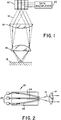
- FIG. 1 is a diagram of a preferred embodiment of multichannel recording apparatus with a laser diode array constructed in accordance with the present invention.
- FIG. 2 is a diagrammatic illustration of the laser diode assembly of FIG. 1 showing the laser diodes edge coupled to channel waveguides.
- FIGS. 3a and 3b are diagrammatic illustrations of the laser diode array of FIG. 1 showing the laser diodes mounted on a silicon substrate.
- FIG. 4 is a diagrammatic view similar to FIGS. 3a and 3b, but illustrating the laser diodes and waveguides on a gallium arsenide substrate.
- FIGS. 5a and 5b illustrate another embodiment of the laser diodes and waveguides on a gallium arsenide substrate similar to FIG. 3, but illustrating a different arrangement of the lasers and waveguides.
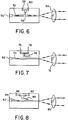
- FIG. 6 illustrates a single laser diode of the laser diode array of FIG. 1 and the associated waveguide to illustrate the signal obtained by a beam splitter.
- FIG. 7 illustrates a single laser diode as does FIG. 6, but illustrating obtaining a signal by coupling from one channel to another using polarization instead of the beam splitter of FIG. 6.
- FIG. 8 is similar to FIGS. 6 and 7, but illustrates a signal obtained by coupling from one channel to another by a tapered edged channel.
- FIG. 9 illustrates an optical system with bulk optics to develop the focus and tracking signals.
- FIG. 10 illustrates another method of obtaining signals wherein reflected light from one channel is reflected into a multimode channel to develop the focus and tracking signals.
- FIG. 11 is similar to FIGS. 9 and 10, but illustrates the use of tapered waveguides for developing signals.
- the data to be recorded is first applied to recording circuity (not shown) which encodes the applied data.
- the encoded data from the recording circuitry is applied to the laser optical system which includes a multisource array 10.
- the multisource array 10 generates laser beams 12 that are collimated by collector lens 14 and focused by objective lens 16 onto the surface of an optical recording disk 18.
- the encoded data is coupled to the array 10 via a data multiplexer 20.
- the focused beam 12 can be regarded as a highly multiplexed data channel with each point in the dynamic image representing an independent data stream so that it is possible to transfer many data channels simultaneously through one optical head in an otherwise conventional optical recording system.
- FIGS. 2-5 illustrate various options for the layout of the multisource array 10 whereby the optical beams 12 from the diode lasers 22 can be brought closer together to a separation of about 10 ⁇ m.
- the diode lasers 22 are edge coupled to waveguides 24.
- the waveguides 24 are curved to bring light beams closer while the diode lasers 22 are separated farther apart.
- the waveguides 24 are preferably constructed of low loss materials so that for a typical propagation distance of about 1 cm, total optical losses are less than about 0.5 decibels.
- coupling efficiencies of 50 percent or greater can be achieved. It has been experimentally determined that coupling efficiencies of over 30 percent are possible without any anti-reflection coatings on the waveguide surfaces when there is precise alignment of the laser diodes 22 with the waveguides 24.
- FIGS. 3a and 3b illustrate another embodiment wherein the waveguides 24′ are fabricated on an oxidized silicon, SiO2, substrate 26 and the diode lasers 22′ are mounted on a silicon substrate 28.
- the laser diodes 22' are mounted on the silicon substrate 28 without a heat sink because the silicon substrate 28 provides a sufficient heat sink.
- Each laser diode 22' has a metal contact 30 mounted on the substrate 28. The metal contact 30 protrudes through a layer of silicon nitrite, SiN4, and extends to contact a layer of gallium aluminum arsenide, GaAlAs, 34.
- the top layer 34 is a layer of gallium arsenide, GaAs, 36 beneath a layer of gallium aluminum arsenide, GaAlAs, 38 which lies below a top layer of gallium arsenide 40.
- coupling efficiencies of greater than 50 percent can be achieved by a proper matching of numerical aperture of the waveguide and a precise alignment of the laser diode 22' to the waveguide 24'. Vertical alignment is made easier because the laser diode 22 is mounted on the same substrate 28 as the waveguide 24'.
- FIG. 4 illustrates another embodiment very similar to FIG. 3 but using a gallium arsenide, GaAs, substrate 28' on which the various layers are grown for fabrication of the laser diode 22".
- a diode facet is etched, preferably using a chemical ion beam assisted technique.
- channel waveguide 24" can be formed in alignment with the laser diode 22" to couple light from the laser diode 22" to the channel waveguide 24".
- the channel waveguide material may need to be modified slightly, by disordering, for example, to decrease the waveguide loss.
- the embodiment of FIG. 4 does not require any precise alignment of the laser diodes 22", and good coupling efficiency, greater than about 60-70 percent, is possible. If the waveguide loss is higher than about 1 decibel per centimeter or otherwise higher than desirable, then during the etching of the laser facets, channels can be etched and dielectric material, such as glass waveguide material, for example, can be used in the channels.
- FIGS. 5a and 5b illustrate another embodiment wherein structures are grown on a gallium arsenide, GaAs, substrate 42 for multichannel recording.
- a laser 44 is grown and a facet is etched thereon, then a channel waveguide 46 is formed with a 90° bend. At the bend there is a mirror 48 that reflects light over 90° due to total internal reflection.
- Several channels can be made this way.
- the channel lengths are preferably short on the order of a few hundred microns so that optical loss is small.
- An alternative is not to etch a facet on the laser 44 thereby letting the 90° bent channel act as a laser cavity. Doing this provides minimum alignments and is easier to fabricate.
- the mechanism for multichannel recording operation includes the plurality of laser diodes wherein each diode is spaced a preselected distance from adjacent diodes and the plurality of channel waveguides that are coupled to the plurality of laser diodes with each channel waveguide then associated with a respective laser diode so that light emitted by the plurality of laser diodes is channeled for convergence at a point outside the waveguides.
- the preselected spacing of the laser beams 12 is less than about 50 ⁇ m which was heretofore unachievable, and, is preferably about 10 ⁇ m.
- the light emitted by the laser diodes is channeled to the collector lens by the channel waveguides.
- the channel waveguides define pathways that may vary in length and some of the waveguides may define straight paths and some may define arcuate paths so that the light emitted by the laser diodes converges at some point after exiting the channels. Preferably, the point of convergence is reached by the light beams prior to reaching the collector lens.
- FIGS. 6-8 illustrate apparatus for detecting the light reflected from the disk surface.
- FIG. 6 illustrates a laser diode 50 and waveguide 52 for emitting and channeling light to the lens 54.
- a beam splitter 56 directs the reflected beam onto detectors 58 and 60.
- One of the drawbacks to the use of the beam splitter 56 is that there is a loss of light and light gets fed to the diode laser 50 also.
- FIG. 6 thus illustrates a means for a multichannel reader wherein a beam splitter 56 is positioned in one of the channel waveguides which channel receives reflected light and detector means 58, 60 for detecting light and reflected light by way of the beam splitter 56.
- FIG. 7 illustrates reading apparatus similar to FIG. 6 but using different elements.
- Light from a laser diode 62 travels through channel waveguide 70 to the collector lens 72 and reflected back to the channel waveguide 70.
- Light is tapped from the channel 70 by another channel 74 where the light is detected by detectors 76 and 78. If the incident beam is of one polarization and the reflected beam of another polarization, then the reflected beam can be coupled into the second channel 74 for detection purposes.
- This method requires a quarterwave plate in the optical system and is not suitable for M-O media detection.
- a tapered channel 80 is used for detection of reflected light.
- Light emanating from laser diode 82 is channeled through channel waveguide 84 to the lens 86 where reflected light from the lens 86 is reflected back to the channel 82.
- the tapered channel 80 directs light to detectors 88 and 90.
- the tapered coupler insures that reflected light traveling in the channel waveguide 84 is channeled to the detectors 88, 90.
- the tapered waveguide approach does not require any polarization change. This should prove to be a good solution for readout signal detection.
- FIGS. 6-8 illustrate means for multichannel reading which includes a plurality of detectors that detect reflected light and a plurality of detector waveguides. Each detector waveguide is associated with a selected one of the detectors and is coupled to a selected one of the channel waveguides so that reflected light travelling in the selected channel waveguide is channeled to the selected detector.
- the means for multichannel reading may include taper coupling and may also include a beam splitter that is positioned in one of the channel waveguides. Detector means are provided for detecting light and reflected light by means of the beam splitter.
- FIGS. 9-11 illustrate apparatus for the detection of tracking and focus signals.
- FIG. 9 illustrates a bulk optics approach wherein there is one channel 92 with bulk optics which will do the focus and tracking signal as illustrated.
- the bulk optics includes a collector lens 94 which receives a light beam 96 from the channel 92 emitted by the channel diode 98.
- the beam 96 passes through a beam splitter 100 and a portion of the light travels to the collector lens 102 where it is directed to the surface of the disk 104.
- a portion of the light from the beam splitter 100 passes through quarterwave plate 106 and to beam splitter 108 where light from a second diode 110 is directed through a lens 112 to the second beam splitter 108.
- the output of the beam splitter 108 is directed to a grating surface 114 and a light therefrom is focused through lens 116 to detectors 118 for focus and tracking.
- FIG. 10 another embodiment is illustrated.
- light reflected from one channel 120 is reflected into a multimode channel 122 to keep the focus and tracking signal information.
- the multimode channel 122 is divided into two channels 124 and 126 to separate the beam for focus error detection and tracking error detection.
- a tracking error signal can be detected by using a split detector and the difference in the signal output of the two detectors gives the tracking error signal.
- the focus error signal can be detected by the total internal reflection method or by a beam size detection method.
- FIG. 10 thus illustrates a means for detecting errors which include a multimode waveguide channel 122 for receiving reflected light and a plurality of detectors 128 coupled to the mode to mode waveguide channel 122 sufficiently to detect focus and tracking errors.
- FIG. 11 also illustrates apparatus for multichannel reading that includes detectors 130, 132, 134 for detecting reflected light and a plurality of detector waveguides 136, 138 140.
- Each of the detector waveguides 136, 138, 140 is associated with a respective detector 130, 132, 134 and is taper coupled to its associated channel waveguide 142, 144, 146 so that reflected light traveling in a selected channel waveguide is channeled to a selected detector.
- reflected light traveling in channel waveguide 142 is taper coupled to detector waveguide 136, which channels light to detector 130.
- the apparatus includes a multisource array that has a plurality of laser diodes which each diode spaced a distance more than about 50 to 100 ⁇ m from adjacent diodes. But, the beams emanating from the waveguides are closely spaced less than about 50 ⁇ m from one another. This closer spacing is achieved without crosstalk or electro interferences because of a plurality of channel waveguides that are coupled to the laser diodes.
- Each channel waveguide is associated with a respective laser for directing the light emitted by the diode toward the optical disk for optical recording and it also receives reflected light from the optical disk for reading the optical disk.
- the arcuate configuration of the waveguides allows beams to be spaced as close as about 10 ⁇ m.
Landscapes
- Physics & Mathematics (AREA)
- Optics & Photonics (AREA)
- General Physics & Mathematics (AREA)
- Engineering & Computer Science (AREA)
- Microelectronics & Electronic Packaging (AREA)
- Optical Head (AREA)
- Optical Integrated Circuits (AREA)
Applications Claiming Priority (2)
| Application Number | Priority Date | Filing Date | Title |
|---|---|---|---|
| US787159 | 1991-11-04 | ||
| US07/787,159 US5195152A (en) | 1991-11-04 | 1991-11-04 | Multichannel optical recording apparatus employing laser diodes |
Publications (2)
| Publication Number | Publication Date |
|---|---|
| EP0541461A2 true EP0541461A2 (fr) | 1993-05-12 |
| EP0541461A3 EP0541461A3 (en) | 1993-06-30 |
Family
ID=25140601
Family Applications (1)
| Application Number | Title | Priority Date | Filing Date |
|---|---|---|---|
| EP19920420390 Withdrawn EP0541461A3 (en) | 1991-11-04 | 1992-10-29 | Multichannel optical recording apparatus employing laser diodes |
Country Status (3)
| Country | Link |
|---|---|
| US (1) | US5195152A (fr) |
| EP (1) | EP0541461A3 (fr) |
| JP (1) | JPH05217194A (fr) |
Cited By (2)
| Publication number | Priority date | Publication date | Assignee | Title |
|---|---|---|---|---|
| EP0836738A4 (fr) * | 1995-07-05 | 1999-09-22 | Yenploy Pty Ltd | Systeme de memorisation optique |
| WO2005027107A1 (fr) * | 2003-09-18 | 2005-03-24 | Koninklijke Philips Electronics N.V. | Support d'information et systeme pour lire des donnees stockees sur un tel support |
Families Citing this family (25)
| Publication number | Priority date | Publication date | Assignee | Title |
|---|---|---|---|---|
| US5289454A (en) * | 1991-12-19 | 1994-02-22 | Minnesota Mining And Manufacturing Company | Optical disc addressing devices a method of use thereof |
| US5278812A (en) * | 1992-02-18 | 1994-01-11 | At&T Bell Laboratories | Tracking and focussing functions in optical disk apparatus |
| EP0620458A4 (fr) * | 1992-09-07 | 1995-02-01 | Nippon Kogaku Kk | Guide d'onde optique et instrument optique l'utilisant. |
| US5617500A (en) * | 1994-05-20 | 1997-04-01 | Nikon Corporation | System for detecting an optical information and scanning microscope system |
| US5835458A (en) * | 1994-09-09 | 1998-11-10 | Gemfire Corporation | Solid state optical data reader using an electric field for routing control |
| GB2312968B (en) * | 1996-05-09 | 2000-09-13 | Daewoo Telecom Ltd | Splicer for light waveguides |
| KR100243134B1 (ko) | 1997-08-30 | 2000-02-01 | 윤종용 | 기록 재생용 광픽업 장치 |
| US6137105A (en) * | 1998-06-02 | 2000-10-24 | Science Applications International Corporation | Multiple parallel source scanning device |
| US6341118B1 (en) * | 1998-06-02 | 2002-01-22 | Science Applications International Corporation | Multiple channel scanning device using oversampling and image processing to increase throughput |
| US6166756A (en) * | 1998-06-02 | 2000-12-26 | Science Applications International Corporation | Multiple channel data writing device |
| US6584052B1 (en) | 1998-06-02 | 2003-06-24 | Science Applications International Corporation | Method and apparatus for controlling the focus of a read/write head for an optical scanner |
| US6091067A (en) * | 1998-06-02 | 2000-07-18 | Science Applications International Corporation | Scanning device using fiber optic bimorph |
| US6246658B1 (en) | 1998-06-02 | 2001-06-12 | Science Applications International Corporation | Multiple channel scanning device using optoelectronic switching |
| EP1376179A3 (fr) * | 2002-06-27 | 2004-04-14 | Toyoda Koki Kabushiki Kaisha | Guide d'ondes optique stratifié, dispositif collecteur de faisceaux lumineux et dispositif émetteur laser |
| US6999484B2 (en) | 2003-03-18 | 2006-02-14 | Eastman Kodak Company | Parallel access data storage system using a combination of VCSEL arrays and an integrated solid immersion lens array |
| JP4792011B2 (ja) * | 2007-06-29 | 2011-10-12 | 日本放送協会 | 光ヘッドおよび光ディスク用記録再生装置 |
| US8248905B2 (en) | 2010-10-15 | 2012-08-21 | General Electric Company | Method of parallel bit-wise holographic data storage source using a parallel light source |
| US8254224B2 (en) | 2010-11-18 | 2012-08-28 | General Electric Company | Servoing system for master with parallel tracks in a holographic replication system |
| US8154975B1 (en) | 2010-11-18 | 2012-04-10 | General Electric Company | Servoing system for multiple spot registration for holographic replication system |
| SG185912A1 (en) * | 2011-05-18 | 2012-12-28 | Agency Science Tech & Res | Alignment method for a silicon photonics packaging |
| US9442248B2 (en) | 2012-03-16 | 2016-09-13 | Nec Corporation | Polarization beam combiner/splitter, polarization beam combining/splitting structure, light mixer, optical modulator module, and method for manufacturing polarization beam combiner/splitter |
| CN104487878A (zh) * | 2012-07-17 | 2015-04-01 | 日本电气株式会社 | 偏振分离器、偏振分离结构、光混合器和偏振分离器的制造方法 |
| US9196278B1 (en) | 2014-05-23 | 2015-11-24 | Seagate Technology Llc | Laser array for heat assisted magnetic recording |
| EP4425153A3 (fr) | 2015-06-12 | 2024-11-20 | Pacific Biosciences Of California, Inc. | Dispositifs et systèmes de guide d'ondes cible intégrés pour couplage optique |
| US12535420B2 (en) | 2020-02-18 | 2026-01-27 | Pacific Biosciences Of California, Inc. | Highly multiplexed nucleic acid sequencing systems |
Family Cites Families (8)
| Publication number | Priority date | Publication date | Assignee | Title |
|---|---|---|---|---|
| US4318058A (en) * | 1979-04-24 | 1982-03-02 | Nippon Electric Co., Ltd. | Semiconductor diode laser array |
| NL8103599A (nl) * | 1981-07-30 | 1983-02-16 | Philips Nv | Inrichting voor het optisch aftasten van een document. |
| EP0092420A1 (fr) * | 1982-04-19 | 1983-10-26 | Xerox Corporation | Systèmes de mémorisation d'information |
| US4428647A (en) * | 1982-11-04 | 1984-01-31 | Xerox Corporation | Multi-beam optical system using lens array |
| EP0345232A3 (fr) * | 1988-05-31 | 1991-07-31 | Nikon Corporation | Appareil optique intégré pour tête d'enregistrement et de reproduction magnéto-optique |
| JP2701403B2 (ja) * | 1988-12-29 | 1998-01-21 | ソニー株式会社 | 光磁気デイスク装置 |
| US4897671A (en) * | 1989-01-23 | 1990-01-30 | Polaroid Corporation | Integrated optic print head |
| US5109447A (en) * | 1991-03-04 | 1992-04-28 | The Boeing Company | High-powered, spectrally flat, very broadband optical source including optical coupler and method using same |
-
1991
- 1991-11-04 US US07/787,159 patent/US5195152A/en not_active Expired - Lifetime
-
1992
- 1992-10-29 EP EP19920420390 patent/EP0541461A3/en not_active Withdrawn
- 1992-11-04 JP JP4295227A patent/JPH05217194A/ja not_active Withdrawn
Cited By (2)
| Publication number | Priority date | Publication date | Assignee | Title |
|---|---|---|---|---|
| EP0836738A4 (fr) * | 1995-07-05 | 1999-09-22 | Yenploy Pty Ltd | Systeme de memorisation optique |
| WO2005027107A1 (fr) * | 2003-09-18 | 2005-03-24 | Koninklijke Philips Electronics N.V. | Support d'information et systeme pour lire des donnees stockees sur un tel support |
Also Published As
| Publication number | Publication date |
|---|---|
| JPH05217194A (ja) | 1993-08-27 |
| US5195152A (en) | 1993-03-16 |
| EP0541461A3 (en) | 1993-06-30 |
Similar Documents
| Publication | Publication Date | Title |
|---|---|---|
| US5195152A (en) | Multichannel optical recording apparatus employing laser diodes | |
| US7184386B2 (en) | Integrated type optical head with sheet waveguide and light coupler | |
| EP0614098B1 (fr) | Dispositif optique | |
| US4779259A (en) | Optical head assembly with efficient light source coupling surface and method of construction | |
| US6487224B1 (en) | Laser diode assembly | |
| US5195150A (en) | Optoelectronic device for outfeed and infeed of radiation | |
| US4945525A (en) | Optical information processing apparatus | |
| KR100313298B1 (ko) | 광학장치 | |
| US5235589A (en) | Apparatus for recording and reproducing optical information and prism coupler | |
| EP1255134B1 (fr) | Prisme composite du type réfléchissant et appareil de lecture optique utilisant ce prisme | |
| EP0814468B1 (fr) | Dispositif optique d'enregistrement et de reproduction | |
| EP0483438B1 (fr) | Structure de tête optique intégrée | |
| EP1130582B1 (fr) | Dispositif laser à semiconducteur et dispositif de lecture optique l'utilisant | |
| KR20000022892A (ko) | 광학 헤드, 기록 및/또는 재생 장치, 및 광학 디스크드라이브 | |
| JPS6273437A (ja) | 光学式ヘツド装置 | |
| US5161148A (en) | Optical pick-up using wavelength guide with grating coupler therein | |
| US5781576A (en) | Semiconductor laser device and optical disk drive | |
| KR20010085724A (ko) | 반도체 레이저 장치, 레이저 결합기, 데이터 재생 장치,데이터 기록 장치 및 반도체 레이저 장치의 제조 방법 | |
| KR20020071737A (ko) | 반도체 레이저 장치 | |
| US5233595A (en) | Optical pickup including waveguide light intensity detection means for controlling a position/intensity of a semiconductor laser | |
| JP2527903B2 (ja) | 多重チャネル・デ―タ記憶装置及び多重チャネル・レ―ザ光学装置 | |
| US6408116B1 (en) | Light guide path element and optical pickup | |
| US5757029A (en) | Triangular pyramidal semiconductor structure and optical device using the same | |
| KR100293464B1 (ko) | 이파장광원모듈및그의제조방법과그를이용한광픽업장치 | |
| JPS62275332A (ja) | 光ヘツド |
Legal Events
| Date | Code | Title | Description |
|---|---|---|---|
| PUAI | Public reference made under article 153(3) epc to a published international application that has entered the european phase |
Free format text: ORIGINAL CODE: 0009012 |
|
| PUAL | Search report despatched |
Free format text: ORIGINAL CODE: 0009013 |
|
| AK | Designated contracting states |
Kind code of ref document: A2 Designated state(s): DE FR GB |
|
| AK | Designated contracting states |
Kind code of ref document: A3 Designated state(s): DE FR GB |
|
| 17P | Request for examination filed |
Effective date: 19931210 |
|
| 17Q | First examination report despatched |
Effective date: 19951219 |
|
| 18D | Application deemed to be withdrawn |
Effective date: 19960430 |