EP0542040A2 - Auslösesteuervorrichtung für einen Schalter - Google Patents
Auslösesteuervorrichtung für einen Schalter Download PDFInfo
- Publication number
- EP0542040A2 EP0542040A2 EP92118438A EP92118438A EP0542040A2 EP 0542040 A2 EP0542040 A2 EP 0542040A2 EP 92118438 A EP92118438 A EP 92118438A EP 92118438 A EP92118438 A EP 92118438A EP 0542040 A2 EP0542040 A2 EP 0542040A2
- Authority
- EP
- European Patent Office
- Prior art keywords
- voltage
- level
- controlled
- logical
- voltage detector
- Prior art date
- Legal status (The legal status is an assumption and is not a legal conclusion. Google has not performed a legal analysis and makes no representation as to the accuracy of the status listed.)
- Granted
Links
Images

Classifications
-
- H—ELECTRICITY
- H02—GENERATION; CONVERSION OR DISTRIBUTION OF ELECTRIC POWER
- H02H—EMERGENCY PROTECTIVE CIRCUIT ARRANGEMENTS
- H02H9/00—Emergency protective circuit arrangements for limiting excess current or voltage without disconnection
- H02H9/04—Emergency protective circuit arrangements for limiting excess current or voltage without disconnection responsive to excess voltage
-
- G—PHYSICS
- G11—INFORMATION STORAGE
- G11C—STATIC STORES
- G11C5/00—Details of stores covered by group G11C11/00
- G11C5/14—Power supply arrangements, e.g. power down, chip selection or deselection, layout of wirings or power grids, or multiple supply levels
- G11C5/143—Detection of memory cassette insertion or removal; Continuity checks of supply or ground lines; Detection of supply variations, interruptions or levels ; Switching between alternative supplies
-
- H—ELECTRICITY
- H02—GENERATION; CONVERSION OR DISTRIBUTION OF ELECTRIC POWER
- H02H—EMERGENCY PROTECTIVE CIRCUIT ARRANGEMENTS
- H02H3/00—Emergency protective circuit arrangements for automatic disconnection directly responsive to an undesired change from normal electric working condition with or without subsequent reconnection ; integrated protection
- H02H3/20—Emergency protective circuit arrangements for automatic disconnection directly responsive to an undesired change from normal electric working condition with or without subsequent reconnection ; integrated protection responsive to excess voltage
- H02H3/207—Emergency protective circuit arrangements for automatic disconnection directly responsive to an undesired change from normal electric working condition with or without subsequent reconnection ; integrated protection responsive to excess voltage also responsive to under-voltage
Definitions
- This invention relates to trip control devices for monitoring the voltage applied on the circuit breakers and to trip the circuit breakers and thereby to protect the voltage source and the loads. More particularly, this invention relates to such trip control devices which render the circuit breakers incapable of being made and closed when the controlled voltage such as the source voltage exhibit abnormal level due to overvoltage.
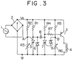
- Fig. 3 is a circuit diagram showing a conventional trip control device, which is disclosed, for example, in Japanese Utility Model Publication (Kokoku) No. 58-18441.
- a controlled power source 1 such as a generator
- the AC voltage supplied from a controlled power source 1 is rectified by a full-wave rectifier 2 consisting of a diode bridge circuit.
- the negative terminal of the full-wave rectifier 2 is grounded, while the positive terminal thereof supplies the controlled voltage V0 to the respective circuit components.
- a PNP type transistor 3 having an emitter coupled to the positive terminal of the full-wave rectifier 2 drives the electromagnetic coil 4.
- One terminal of the electromagnetic coil 4 is coupled to the collector of the transistor 3, while the other terminal thereof is grounded.
- the electromagnetic coil 4 is energized and de-energized by turning on and off the transistor 3.
- the electromagnetic coil 4 is de-energized to trip the circuit breaker (not shown) when the controlled voltage V0 becomes less than the predetermined level.
- the circuit breaker associated with the electromagnetic coil 4 can be made only when the electromagnetic coil 4 is energized. The circuit breaker cannot be made when the electromagnetic coil 4 is de-energized.
- the gate of an N-gate thyristor 5 coupled in series with a resistor R1 across the full-wave rectifier 2 is controlled by a voltage at a middle point A of the voltage divider consisting of a resistor R2 and a variable resistor R3.
- a Zener diode 6 is coupled across the N-gate thyristor 5 in opposite polarity.
- the gate of a P-gate thyristor 7 coupled in series with a resistor R4 across the full-wave rectifier 2 is controlled through a Zener diode 9 by the voltage at the middle point B of the voltage divider consisting of a resistor R5 and a variable resistor R6.
- a capacitor 8 is coupled across the anodes of the N-gate thyristor 5 and P-gate thyristor 7.
- a resistor R7 connects the anode of the P-gate thyristor 7 and the point B coupled to the base of the transistor 3.
- the operation of the circuit of Fig. 3 is as follows. Before the voltage is supplied from the controlled power source 1, the P-gate thyristor 7 is turned off. Thus, so long as the controlled voltage V0 is low, the base voltage of the transistor 3 remains at the high level, such that the transistor 3 is kept turned off. The electromagnetic coil 4 is thus de-energized and the circuit breaker is tripped and is incapable of making.
- the circuit breaker associated with the electromagnetic coil 4 thus becomes capable of being made.
- the first minimum excitation voltage level for turning on the electromagnetic coil 4 can be set by adjusting the voltage at the divider point B by means of the variable resistor R6.
- the N-gate thyristor 5 When the P-gate thyristor 7 is turned on, the N-gate thyristor 5 is forcibly turned off by the commutation current of the capacitor 8. The P-gate thyristor 7 remains turned off until the controlled voltage V0 falls below a second minimum excitation voltage level. When the controlled voltage V0 falls below the second minimum excitation voltage level, the voltage at the divider point A coupled to the gate of the N-gate thyristor 5 becomes less than the voltage of the Zener diode 6, namely, the voltage at the anode of the N-gate thyristor 5. As a result, the N-gate thyristor 5 is turned on, and the commutation current from the capacitor 8 turns off the P-gate thyristor 7. The transistor 3 is thus turned off and the electromagnetic coil 4 is de-energized, such that the circuit breaker is tripped and becomes incapable of being made.
- the second minimum excitation voltage level for triggering the tripping operation in the case of abnormal low voltage is set lower than the first minimum excitation voltage level such that the circuit exhibit hysteresis and the operation is stabilized.
- the electromagnetic coil 4 is again energized as described above.
- the above trip control device for a circuit breaker has the following disadvantage.
- the circuit breaker is tripped (i.e., rendered incapable of being made) only when an abnormal low level of the controlled voltage V0 is detected.
- the circuit breaker is not tripped and remains capable of being made.
- the destruction of expensive equipment or a grave failure accident such as fire may ensue.
- a trip control device for a circuit breaker which comprises an electromagnetic coil which is energized to render a circuit breaker capable of being made when a voltage applied thereacross exceeds a minimum excitation voltage level; a drive circuit for selectively energizing and de-energizing the electromagnetic coil, the drive circuit energizing the electromagnetic coil when turned on, and de-energizing the electromagnetic coil when turned off; and voltage detector means for detecting a controlled voltage and for turning off the drive circuit when the controlled voltage exceeds a maximum allowable voltage level, and turning off the drive circuit when the controlled voltage falls from the maximum allowable voltage level to an operation resumable level.
- the voltage detector means comprises: a first voltage detector for detecting a first reference voltage corresponding to the maximum allowable voltage level, the first voltage detector outputting a first signal at logical level 1 when the controlled voltage exceeds the first reference voltage; a second voltage detector for detecting a second reference voltage corresponding to the operation resumable level, the second voltage detector outputting a second signal at logical level 1 when the controlled voltage exceeds the second reference voltage, and at logical level 0 when the controlled voltage falls below the second reference voltage, wherein the second reference voltage is higher than the first reference voltage; means, coupled to the second voltage detector, for reducing the first signal to logical level 0 upon receiving the second signal at logical level 1; and a logical OR circuit for generating a logical sum of an output of the first voltage detector and an output of the second voltage detector, the logical sum turning off the drive circuit when at logical 1 and turning on the drive circuit when at logical level 0.
- the reducing means includes means for delaying reducing operation for a predetermined time length upon receiving the second signal at logical level 1.
- Fig. 1 is a circuit diagram showing a trip control device according to this invention.
- the parts 1 through 4 are similar to the corresponding parts 1 through 4 in Fig. 3.
- the drive circuit 3 consists of a transistor and selectively energizes and de-energizes the electromagnetic coil 4.
- the drive circuit 3 is conducting (turned on) at the initial state before the voltage is supplied.
- the electromagnetic coil 4 is automatically energized and renders the associated circuit breaker capable of being made when the controlled voltage V0 exceeds a minimum excitation voltage level.
- a resistor R10 is inserted between the controlled power source 1 and an input terminal of full-wave rectifier 2.
- the resistor R10 may be omitted when the same function is provided by the impedance within the controlled power source 1.
- the voltage divider consisting of a resistor R11 and a variable resistor R12 and coupled across the output terminals of the full-wave rectifier 2 provide a first divider voltage at point C for detecting the first reference voltage V1 corresponding to the maximum allowable voltage level of the controlled voltage V0.
- the voltage divider consisting of a resistor R13 and a variable resistor R14 and coupled across the output terminals of the full-wave rectifier 2 provide a second divider voltage at point D for detecting the second reference voltage V2 corresponding to the operation resumable level of the controlled voltage V0.
- a first voltage detector 11 detects the voltage at the divider point C and outputs a high level signal T1 (at the logical level 1) when the controlled voltage Va exceeds the first reference voltage V1 to raise the voltage at point C above the threshold voltage level thereof.
- a second voltage detector 12 detects the voltage at the divider point D and outputs a high level signal T2 (at the logical level 1) when the controlled voltage V0 exceeds the second reference voltage V2 to raise the voltage at point D above the threshold voltage level thereof.
- the output signal T2 of the second voltage detector 12 is reduced to the low level (logical level 0) when the controlled voltage V0 falls below the second reference voltage V2.
- An OR gate 13 generates the logical sum of the outputs T1 and T2 of the first voltage detector 11 and the second voltage detector 12. Thus the trip signal T output from the OR gate 13 is at the high level when either the signal T1 or T2 is at the high level.
- the transistor 3 is turned on and off by the trip signal T.
- a NPN type transistor 14 is coupled across the variable resistor R12.
- the emitter of the transistor 14 is grounded, while the output signal T2 from the second voltage detector 12 is applied to the base thereof.
- the transistor 14 is turned on when the output T2 is at the high level, thereby grounding the point C.
- the output T1 of the first voltage detector 11 is reduced to the low level.
- a capacitor 15 coupled across the variable resistor R12 prevents abrupt rise of voltage at point C when the controlled voltage V0 returns to operation resumable level and the transistor 14 is turned off.
- the electromagnetic coil 4 exhibits a predetermined impedance, and the serial circuit of the impedance of the controlled power source 1 or that of the resistor R10 and the impedance of the electromagnetic coil 4 determines the controlled voltage V0 developed across the electromagnetic coil 4 or the output terminals of the full-wave rectifier 2.
- the controlled voltage V0 is applied across the voltage divider consisting of the resistors R11 and R12 to develop a corresponding voltage at point C, and across the voltage divider consisting of the resistors R13 and R14 to develop a corresponding voltage at point D.
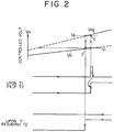
- Fig. 2 shows the controlled voltage level (at the top) and signal waveforms T1 and T2 in the circuit of Fig. 1 upon tripping (at the middle) and upon resuming operation (at the bottom).
- the operation of the circuit of Fig. 1 up to the point when the electromagnetic coil 4 is de-energized to trip the associated circuit breaker (render it incapable of being made) is as follows.
- the voltages at the divider points C and D are both low and thus the outputs T1 and T2 of the first voltage detector 11 and the second voltage detector 12 are both at the low level. Consequently, the trip signal T output from the OR gate 13 is also at the low level, and the transistor 3 is turned on and conducting.
- the electromagnetic coil 4 is energized to render the associated circuit breaker capable of being made.
- the minimum excitation voltage level is at about 80 percent of the rated voltage with respect to the source voltage of the controlled power source 1.
- the controlled power source 1 is placed under normal load condition when the transistor 3 is turned on and the electromagnetic coil 4 is energized. Assume that the controlled voltage under the normal load condition rises gradually as shown at V01 at the top in Fig. 2.
- the controlled voltage V01 under normal load reaches and exceeds the first reference voltage V1 corresponding to the maximum allowable voltage level
- the voltage at the point C rises above a threshold level of the first voltage detector 11, and the output T1 of the first voltage detector 11 rises to the high level.
- the trip signal T output from the OR gate 13 also rises to the high level to turn off the transistor 3.
- the first reference voltage V1 corresponding to the maximum allowable voltage level is at about 125 percent of the rated voltage with respect to the source voltage.
- the voltage at divider point C for detecting the first reference voltage V1 is adjusted by the variable resistor R12.
- the electromagnetic coil 4 is thus de-energized and the controlled power source 1 transits to the light load condition.
- the controlled voltage rises abruptly toward point c as shown by an upward vertical arrow in Fig. 2.
- the controlled voltage under the light load is represented by V02 in Fig. 2.
- the high level signal T2 maintains the output T of the OR gate 13 at the high level, and, at the same time, the high level signal T2 turns on the transistor 14 and thereby grounds the point C coupled to the input of the first voltage detector 11. As a result, the output T1 of the first voltage detector 11 is reduced to the low level. Under this circumstance, the output T of the OR gate 13 is maintained at the high level exclusively due to the high level of the output T2 of the second voltage detector 12 and thus keeps the electromagnetic coil 4 de-energized. Thus, the voltage detector circuit is in the "resumable level detection mode" for detecting the resumable level, as described in detail below. After the jump upon the controlled voltage exceeding the first reference voltage V1, the controlled voltage V02 under light load may continue to rise as shown in Fig. 2.
- the resuming operation of the circuit of Fig. 1 is described. Assume that the controlled voltage under light load V02 falls to the second reference voltage V2, moving along the curve V02 toward left as represented in Fig. 2. Then, the voltage at point D falls below the threshold level of the second voltage detector 12 and the output T2 thereof returns to the low level, thereby reducing the output T of the OR gate 13 also to the low level. The transistor 3 is thus turned on and the electromagnetic coil 4 is energized to render the circuit breaker capable of being made.
- the second reference voltage V2 corresponding to the resumable voltage level is set at 120 percent of the rated voltage with respect to the source voltage.
- the voltage at the divider point D for detecting the second voltage V2 is adjusted by the variable resistor R14. For the purpose of ensuring stable tripping and resuming operation, the reference voltages for the two operations are designed to exhibit hysteresis of five percent.
- the controlled power source 1 is again under the normal load and the controlled voltage falls abruptly toward point d as shown downward vertical arrow in Fig. 2.
- the transistor 14 is turned off, such that the proper voltage at the divider point C is applied to the input of the first voltage detector 11.
- the output T1 remains at the low level since the controlled voltage falls below the first reference voltage V1.
- the voltage at the point C begins to rise immediately after the transistor 14 is turned off, there is a rise delay due to the charging of the capacitor 15.
- the rise delay of the voltage at the point C due to the capacitor 15 is designed at a sufficient length for covering the time interval in which the controlled voltage V02 under the light load falls to the controlled voltage V01 (at point d ) under the normal load, the voltage at point C after the controlled voltage V01 settles to the point d is applied to the first voltage detector 11. Then, the unstable operation caused by the erroneous detection above the first voltage V1 by the first voltage detector 11 immediately after the detection of the second voltage V2 by the second voltage detector 12 can be prevented.
- the controlled voltage varies in accordance with the variation of the load, from the first state where only the impedance of the resistor R10 is coupled across the controlled power source 1, to the second state where both the impedances of the resistor R10 and the electromagnetic coil 4 are coupled across the controlled power source 1.
- this variation of the controlled voltage is exploited to detect the source voltage level accurately with a simple circuit structure.
- the electromagnetic coil 4 is automatically de-energized when the controlled voltage V0 falls below the minimum excitation voltage level.
- the trip control device can effect the trip operation of the circuit breaker at the minimum excitation voltage level as well.
- the circuit breaker is tripped upon detection of the first voltage V1
- the controlled voltage rises abruptly from the controlled voltage under normal load V01 to the controlled voltage under light load V02.
- the margin for the detection of second voltage V2 is increased, and stable on/off operation of the transistor 3 and the electromagnetic coil 4 is ensured.
- the controlled power source 1 in the above embodiment is an AC power source
- the power source may also be a DC power source.
- the apparatus controlled by the trip control device according to this invention may be an apparatus other than a circuit breaker, provided that the apparatus can be made (closed) and tripped (rendered incapable of being made).
- the electromagnetic coil 4 may be replaced by a device exhibiting a predetermined impedance, such as an input transformer of a power source.
- the power is supplied directly from the controlled power source 1.
- the power may be supplied through a transformer.
- the impedance of the transformer may serve as the resistor R10, and the resistor R10 may hence be omitted.
Landscapes
- Engineering & Computer Science (AREA)
- Power Engineering (AREA)
- Emergency Protection Circuit Devices (AREA)
- Protection Of Static Devices (AREA)
Applications Claiming Priority (2)
| Application Number | Priority Date | Filing Date | Title |
|---|---|---|---|
| JP294382/91 | 1991-11-11 | ||
| JP3294382A JPH05137253A (ja) | 1991-11-11 | 1991-11-11 | 異常電圧検出制御装置 |
Publications (3)
| Publication Number | Publication Date |
|---|---|
| EP0542040A2 true EP0542040A2 (de) | 1993-05-19 |
| EP0542040A3 EP0542040A3 (en) | 1993-09-29 |
| EP0542040B1 EP0542040B1 (de) | 1997-01-02 |
Family
ID=17807005
Family Applications (1)
| Application Number | Title | Priority Date | Filing Date |
|---|---|---|---|
| EP92118438A Expired - Lifetime EP0542040B1 (de) | 1991-11-11 | 1992-10-28 | Auslösesteuervorrichtung für einen Schalter |
Country Status (6)
| Country | Link |
|---|---|
| US (1) | US5375032A (de) |
| EP (1) | EP0542040B1 (de) |
| JP (1) | JPH05137253A (de) |
| KR (1) | KR960003201B1 (de) |
| DE (1) | DE69216370T2 (de) |
| TW (1) | TW222357B (de) |
Cited By (3)
| Publication number | Priority date | Publication date | Assignee | Title |
|---|---|---|---|---|
| ES2155363A1 (es) * | 1998-12-17 | 2001-05-01 | Sanchez Pablo Garrido | Protectores generales de subidas o bajadas de tension por fallos del neutro u otras causas. |
| ES2158781A1 (es) * | 1998-12-17 | 2001-09-01 | Sanchez Pablo Garrido | Dispositivos para las subidas, bajadas o subidas y bajadas de la tension de la red. |
| EP1326250A3 (de) * | 2001-12-27 | 2004-01-21 | Kabushiki Kaisha Toshiba | Spannungsüberwachungssteuerungschaltungsanordnung, Speichersteuerungsanordnung und Speicherkarte unter Verwendung solches |
Families Citing this family (10)
| Publication number | Priority date | Publication date | Assignee | Title |
|---|---|---|---|---|
| DE4313532B4 (de) * | 1993-04-24 | 2007-08-30 | Robert Bosch Gmbh | Verfahren zur Überprüfung einer Endstufe |
| JP3496982B2 (ja) * | 1994-07-15 | 2004-02-16 | 三菱電機株式会社 | 電磁接触器 |
| FR2786919B1 (fr) * | 1998-12-07 | 2001-01-12 | Schneider Electric Ind Sa | Dispositif de commande d'un electro-aimant d'ouverture ou de fermeture d'un disjoncteur, avec commande locale et telecommande |
| KR20000054265A (ko) * | 2000-05-30 | 2000-09-05 | 김천연 | 전자기적 트립 장치를 구비한 차단기 |
| JP4057260B2 (ja) * | 2001-08-07 | 2008-03-05 | 株式会社日立製作所 | 電源回路、電源システム、および電子装置 |
| JP3833600B2 (ja) * | 2002-10-08 | 2006-10-11 | 三菱電機株式会社 | 車両用交流発電機故障判定装置 |
| DE102004059455A1 (de) * | 2004-12-09 | 2006-06-22 | Puls Gmbh | Schaltungsanordnung zur Überspannungserkennung und Verfahren zum Betrieb der Schaltungsanordnung |
| US7852051B2 (en) * | 2005-01-18 | 2010-12-14 | Puls Gmbh | Current-limiting circuit and method for operating the circuit |
| US7554796B2 (en) * | 2006-01-20 | 2009-06-30 | Adc Telecommunications, Inc. | Modular power distribution system and methods |
| CN110197780B (zh) * | 2019-06-05 | 2021-01-12 | 厦门立林电气控制技术有限公司 | 一种脱扣器线圈断线监视电路 |
Family Cites Families (4)
| Publication number | Priority date | Publication date | Assignee | Title |
|---|---|---|---|---|
| GB2139436B (en) * | 1983-03-17 | 1986-10-08 | Janan Emmanuel Allos | Mains protection device |
| US4879625A (en) * | 1987-12-11 | 1989-11-07 | Potenzone Richard A | Voltage monitor |
| US4918562A (en) * | 1989-01-30 | 1990-04-17 | Pulizzi Engineering, Inc. | Power controller with voltage-controlled circuit breaker |
| US4999730A (en) * | 1989-05-10 | 1991-03-12 | Pickard Harold W | Line voltage monitor and controller |
-
1991
- 1991-11-11 JP JP3294382A patent/JPH05137253A/ja active Pending
-
1992
- 1992-06-24 TW TW081104956A patent/TW222357B/zh active
- 1992-06-30 KR KR1019920011513A patent/KR960003201B1/ko not_active Expired - Fee Related
- 1992-10-26 US US07/966,445 patent/US5375032A/en not_active Expired - Fee Related
- 1992-10-28 DE DE69216370T patent/DE69216370T2/de not_active Expired - Fee Related
- 1992-10-28 EP EP92118438A patent/EP0542040B1/de not_active Expired - Lifetime
Cited By (6)
| Publication number | Priority date | Publication date | Assignee | Title |
|---|---|---|---|---|
| ES2155363A1 (es) * | 1998-12-17 | 2001-05-01 | Sanchez Pablo Garrido | Protectores generales de subidas o bajadas de tension por fallos del neutro u otras causas. |
| ES2158781A1 (es) * | 1998-12-17 | 2001-09-01 | Sanchez Pablo Garrido | Dispositivos para las subidas, bajadas o subidas y bajadas de la tension de la red. |
| EP1326250A3 (de) * | 2001-12-27 | 2004-01-21 | Kabushiki Kaisha Toshiba | Spannungsüberwachungssteuerungschaltungsanordnung, Speichersteuerungsanordnung und Speicherkarte unter Verwendung solches |
| US7196944B2 (en) | 2001-12-27 | 2007-03-27 | Kabushiki Kaisha Toshiba | Voltage detection circuit control device, memory control device with the same, and memory card with the same |
| US7203104B2 (en) | 2001-12-27 | 2007-04-10 | Kabushiki Kaisha Toshiba | Voltage detection circuit control device, memory control device with the same, and memory card with the same |
| CN100409369C (zh) * | 2001-12-27 | 2008-08-06 | 株式会社东芝 | 电压检测电路控制设备及其存储器控制设备和存储卡 |
Also Published As
| Publication number | Publication date |
|---|---|
| TW222357B (de) | 1994-04-11 |
| US5375032A (en) | 1994-12-20 |
| KR960003201B1 (ko) | 1996-03-06 |
| DE69216370T2 (de) | 1997-04-24 |
| DE69216370D1 (de) | 1997-02-13 |
| JPH05137253A (ja) | 1993-06-01 |
| EP0542040B1 (de) | 1997-01-02 |
| KR930011362A (ko) | 1993-06-24 |
| EP0542040A3 (en) | 1993-09-29 |
Similar Documents
| Publication | Publication Date | Title |
|---|---|---|
| US4363064A (en) | Overcurrent protection system | |
| KR100299014B1 (ko) | 광대역노이즈면역성을갖는접지고장회로차단기 | |
| US5615097A (en) | Transient over voltage protection circuit for electrical power converters | |
| EP0667666B1 (de) | Stromversorgungseinrichtung mit Einschaltstrombegrenzungsschaltung | |
| CA2071405C (en) | Fault detection apparatus for a transformer isolated transistor drive circuit for a power device | |
| JP2784463B2 (ja) | 交流ライン安定化回路 | |
| US5784231A (en) | Overvoltage protection for SMPS based on demagnetization signal | |
| US4685020A (en) | Shutdown circuit for blocking oscillator power supply | |
| EP0084245A1 (de) | Überstromschutzanordnung für eine Schaltreglerstromquelle | |
| US5375032A (en) | Trip control device for circuit breaker | |
| US4453193A (en) | Overcurrent protection for push-pull circuits | |
| EP0021472A1 (de) | Überspannungsbegrenzer für eine Starkstromleitung | |
| WO1984003182A1 (en) | A fault protection system for power supplies that use ferro-resonant transformers | |
| US5610532A (en) | Isolated DC fault current sensor | |
| US4590533A (en) | Overvoltage protective relay device | |
| US4965692A (en) | Overload detector and protection circuit | |
| US5416692A (en) | AC power supplying unit with self monitoring of AC out and detection of leakage | |
| EP0385544A1 (de) | Geschaltete Speisespannungsschaltung | |
| CA1070762A (en) | D.c. to a.c. electronic inverter with overload protection | |
| US4755923A (en) | Regulated high-voltage power supply | |
| KR102113404B1 (ko) | Smps용 단락 보호 장치 | |
| US4450516A (en) | Device for controlling the regulating facilities in an electric high-power AC-DC converter | |
| JP3010605B2 (ja) | スイッチング電源装置 | |
| JPH03239163A (ja) | 電圧形インバータ | |
| JP3224069B2 (ja) | 静止形過電流検出装置 |
Legal Events
| Date | Code | Title | Description |
|---|---|---|---|
| PUAI | Public reference made under article 153(3) epc to a published international application that has entered the european phase |
Free format text: ORIGINAL CODE: 0009012 |
|
| AK | Designated contracting states |
Kind code of ref document: A2 Designated state(s): DE FR GB NL |
|
| PUAL | Search report despatched |
Free format text: ORIGINAL CODE: 0009013 |
|
| AK | Designated contracting states |
Kind code of ref document: A3 Designated state(s): DE FR GB NL |
|
| 17P | Request for examination filed |
Effective date: 19940204 |
|
| 17Q | First examination report despatched |
Effective date: 19951117 |
|
| GRAG | Despatch of communication of intention to grant |
Free format text: ORIGINAL CODE: EPIDOS AGRA |
|
| GRAH | Despatch of communication of intention to grant a patent |
Free format text: ORIGINAL CODE: EPIDOS IGRA |
|
| GRAH | Despatch of communication of intention to grant a patent |
Free format text: ORIGINAL CODE: EPIDOS IGRA |
|
| GRAA | (expected) grant |
Free format text: ORIGINAL CODE: 0009210 |
|
| AK | Designated contracting states |
Kind code of ref document: B1 Designated state(s): DE FR GB NL |
|
| REF | Corresponds to: |
Ref document number: 69216370 Country of ref document: DE Date of ref document: 19970213 |
|
| ET | Fr: translation filed | ||
| REG | Reference to a national code |
Ref country code: GB Ref legal event code: 727 |
|
| REG | Reference to a national code |
Ref country code: GB Ref legal event code: 727A |
|
| REG | Reference to a national code |
Ref country code: GB Ref legal event code: 727H |
|
| PLBE | No opposition filed within time limit |
Free format text: ORIGINAL CODE: 0009261 |
|
| STAA | Information on the status of an ep patent application or granted ep patent |
Free format text: STATUS: NO OPPOSITION FILED WITHIN TIME LIMIT |
|
| 26N | No opposition filed | ||
| PGFP | Annual fee paid to national office [announced via postgrant information from national office to epo] |
Ref country code: FR Payment date: 19981009 Year of fee payment: 7 |
|
| PGFP | Annual fee paid to national office [announced via postgrant information from national office to epo] |
Ref country code: NL Payment date: 19981028 Year of fee payment: 7 |
|
| PGFP | Annual fee paid to national office [announced via postgrant information from national office to epo] |
Ref country code: GB Payment date: 19981030 Year of fee payment: 7 |
|
| PGFP | Annual fee paid to national office [announced via postgrant information from national office to epo] |
Ref country code: DE Payment date: 19981106 Year of fee payment: 7 |
|
| PG25 | Lapsed in a contracting state [announced via postgrant information from national office to epo] |
Ref country code: GB Free format text: LAPSE BECAUSE OF NON-PAYMENT OF DUE FEES Effective date: 19991028 |
|
| PG25 | Lapsed in a contracting state [announced via postgrant information from national office to epo] |
Ref country code: NL Free format text: LAPSE BECAUSE OF NON-PAYMENT OF DUE FEES Effective date: 20000501 |
|
| GBPC | Gb: european patent ceased through non-payment of renewal fee |
Effective date: 19991028 |
|
| PG25 | Lapsed in a contracting state [announced via postgrant information from national office to epo] |
Ref country code: FR Free format text: LAPSE BECAUSE OF NON-PAYMENT OF DUE FEES Effective date: 20000630 |
|
| NLV4 | Nl: lapsed or anulled due to non-payment of the annual fee |
Effective date: 20000501 |
|
| PG25 | Lapsed in a contracting state [announced via postgrant information from national office to epo] |
Ref country code: DE Free format text: LAPSE BECAUSE OF NON-PAYMENT OF DUE FEES Effective date: 20000801 |
|
| REG | Reference to a national code |
Ref country code: FR Ref legal event code: ST |