EP0542156B1 - Méthode de mise à jour de données emmagasinées dans des locations d'emmagasinage d'un EPROM-Flash - Google Patents
Méthode de mise à jour de données emmagasinées dans des locations d'emmagasinage d'un EPROM-Flash Download PDFInfo
- Publication number
- EP0542156B1 EP0542156B1 EP92119067A EP92119067A EP0542156B1 EP 0542156 B1 EP0542156 B1 EP 0542156B1 EP 92119067 A EP92119067 A EP 92119067A EP 92119067 A EP92119067 A EP 92119067A EP 0542156 B1 EP0542156 B1 EP 0542156B1
- Authority
- EP
- European Patent Office
- Prior art keywords
- updating
- data
- storage locations
- updating information
- storage
- Prior art date
- Legal status (The legal status is an assumption and is not a legal conclusion. Google has not performed a legal analysis and makes no representation as to the accuracy of the status listed.)
- Expired - Lifetime
Links
- 238000003860 storage Methods 0.000 title claims abstract description 89
- 238000000034 method Methods 0.000 title claims abstract description 33
- 230000000694 effects Effects 0.000 abstract description 2
- 230000009467 reduction Effects 0.000 abstract description 2
- 230000015654 memory Effects 0.000 description 23
- 230000008859 change Effects 0.000 description 5
- 238000013500 data storage Methods 0.000 description 4
- 230000008901 benefit Effects 0.000 description 2
- 230000003287 optical effect Effects 0.000 description 2
- 230000009471 action Effects 0.000 description 1
- 230000006399 behavior Effects 0.000 description 1
- 230000010354 integration Effects 0.000 description 1
- 238000004519 manufacturing process Methods 0.000 description 1
- 239000011159 matrix material Substances 0.000 description 1
- 238000004321 preservation Methods 0.000 description 1
- 230000008569 process Effects 0.000 description 1
- 239000007787 solid Substances 0.000 description 1
- 238000012795 verification Methods 0.000 description 1
- 239000002699 waste material Substances 0.000 description 1
Images


Classifications
-
- G—PHYSICS
- G11—INFORMATION STORAGE
- G11C—STATIC STORES
- G11C16/00—Erasable programmable read-only memories
- G11C16/02—Erasable programmable read-only memories electrically programmable
- G11C16/06—Auxiliary circuits, e.g. for writing into memory
- G11C16/10—Programming or data input circuits
- G11C16/102—External programming circuits, e.g. EPROM programmers; In-circuit programming or reprogramming; EPROM emulators
- G11C16/105—Circuits or methods for updating contents of nonvolatile memory, especially with 'security' features to ensure reliable replacement, i.e. preventing that old data is lost before new data is reliably written
-
- G—PHYSICS
- G11—INFORMATION STORAGE
- G11C—STATIC STORES
- G11C16/00—Erasable programmable read-only memories
- G11C16/02—Erasable programmable read-only memories electrically programmable
- G11C16/06—Auxiliary circuits, e.g. for writing into memory
- G11C16/10—Programming or data input circuits
- G11C16/102—External programming circuits, e.g. EPROM programmers; In-circuit programming or reprogramming; EPROM emulators
Definitions
- the present invention relates to a method of updating data stored in storage locations of a storage unit, in particular of a Flash EPROM.
- Each disk reader includes a logic circuit for controlling the disk write physical operations. Normally as soon as a writing or updating command is received, a write physical operation occurs. This method normally involves an enormous waste of time due to the fact that consecutive write logic operations correspond to consecutive write physical operations on different and often distant physical areas of the disk, and therefore a long time is consumed for moving heads from one disk area to another.
- Flash EPROMs are a special type of EEPROMs whose cost is remarkably lower than conventional EEPROMs and moreover the attainable integration degree on a chip is higher (256 kbytes per chip against 32 kbytes per chip).
- Flash EPROMs must be erased totally (like UV EPROMs), i.e. erasure concerns the entire chip, by a simple electrical command, whilst EPROMs are erased on a byte by byte basis; both types of memories are written on a byte by byte basis.
- Flash EPROMs An important feature of Flash EPROMs lies in that it is possible to change the value of any bit from 1 to 0 (programming operating) but it is necessary to erase the entire memory device (erase operation) in order to change the value of a bit from 0 to 1.
- the erase operation goes on for some seconds and consists in turning to 1 all bits of the memory device; Flash EPROM manufactures, e.g. Advanced Micro Devices, recommend to turn, via software or firmware, all the bits of the memory device to 0 before executing such erasing operation in such a way that the locations of the memory device are "consumed" uniformly.
- German Patent Application DE 3741278 discloses an arrangement such as to assure an error-free operation for an EEPROM subjected to a number of erasure/write cycles greater than those allowed for individual locations of EEPROM itself.
- the invention as disclosed in the above-mentioned German Patent Application is based upon a store having a capacity greater than the number of memory zones (comprising several bytes) each time necessary for data to be stored at the same time, and consists first of all in storing data in a single memory zone and then in switching, according to a suitable criterion, on a successive memory zone under the control of a memory controller, and use this successive memory zone until such suitable criterion suggests otherwise; hence it is substantially a question of operative environment change.
- the method as disclosed in the above-mentioned patent application, requires memories of much higher capacity than really needed and moreover it does not solve the problem of quick updating the stored data.
- the japanese patent abstract JPA59071159 discloses a method to correct the information content of an EEPROM memory by reading all the information to a RAM on an IC card processor and by editing in real time the data to be corrected before rewriting the information content on the EEPROM.
- This method does not allow for any time saving or writing EEPROM cycle saving, since the rewrite cycles are equal to the information updating operations, thus leading to a decrease of EEPROM lifetime and longer overall process time.
- the data to be written are stored into a RAM cache memory and a working disk.
- This method and apparatus aims to increase the effective lifetime of the data optical disks and to backup data in case data optical disk failure. It is described thet the cache memory is a continuosly operating storage means, with the data replica on the working disk.
- a remarkable reduction in updating time can be attained by writing information relative to updating to be carried out into not occupied storage locations and executing the updating all at once on the storage locations containing data.
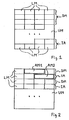
- UM stands for a generic storage unit. Such storage unit UM is organized in storage locations LM. Data are normally written into the memory starting either from the smallest address, as illustrated in figs. 1 and 2, or from the greatest one, and constitute the stored data DM. Consecutive storage locations LM are often used, but in general the control of memory allocation is entrusted to software or firmware.
- Stored data DM are updated, either by software of firmware, by sending write commands, more properly "overwrite” ones, consisting of the data address to be updated and the new binary value of the data itself, to the storage unit UM.
- a high gain in efficiency is obtained by loading updating information IA into not occupied, i.e. virgin, storage locations LM.
- updating information IA generally consists in a number of updatings, stored data DM, accumulated in course of time.
- the loaded updating information IA can be read out, either occasionally or periodically, and used for updating effectively the stored data DM which such updating information IA is referred to.
- updating information IA and stored data DM alternate in the storage locations LM.
- a first possibility, illustrated in fig.1, is to write consecutively all updating information in a well defined storage area independently from the fact that they refer to well defined storage locations.
- the updating information shall contain at least a first sequence of bits containing the address of the storage location to be updated, and a second sequence of bits containing the new binary value of the storage location to be updated.
- a third sequence of bits containing the number of storage locations in which the content is to be updated, in also needed; the first sequence of bits correspond now to starting address of consecutive storage locations and the second sequence of bits will be the new global binary value.
- Updating information IA generally will include a plurality of such sequences of bits.
- a second possibility, illustrated in fig. 2, is to dedicate to a first storage area AM1 a second storage area AM2 capable of containing updating information IA relative to the first storage area AM1.
- the updating information shall contain only a sequence of bits corresponding to the new binary value of the first storage area AM1.
- the advantage in time lies in that loading of updating information IA into not occupied storage locations is not time consuming operation and the total erasure of the device occurs only when a number, pre-establisched by software or firmware, of updatings have to be executed, or at regular intervals, contrary to what was contemplated in the methods used up to now wherein an erasure for each updating was carried out.
- the first example refers to figs. 3 to 7.
- the first storage location is indicated by AM1 and corresponds to the first storage area to be updated.
- the second storage location is indicated by AM2 and corresponds to the second storage area which has to contain the new binary value.
- both storage locations are virgin and their binary value is FF (see fig. 3), as happens in Flash EPROM memories.
- the first storage location stores the binary value 1C (see fig. 4).
- the evolution of the software involves then the need of updating the binary value of the first storage location to A3.
- the method according to the present invention teaches that such new binary value shall not overwrite the old one but it must be loaded into the second storage location, see fig.5.
- data 1C stored will be updated with the new one A3 (see fig. 6) and then the second storage location will he reset to its initial binary value FF, see fig. 7.
- Flash EPROMs when software or firmware decides at a well precise moment to apply updatings, it copies the content of the entire flash EPROM memory into an RAM memory, usually identical to the first one; therefore fig. 5 represents at the same time the content of two storage locations of Flash EPROM and RAM.
- the content A3 of the second storage location, of RAM is copied into the first storage location of RAM, as illustrated in fig.6.
- the content of the second storage location of RAM is reset to FF, as shown in fig. 7.
- Flash EPROM is erased completely and then is programmed by using the content of the RAM memory.
- the contents of Flash EPROM and RAM will be identical; therefore fig. 7 represents at the same time the content of two storage locations of Flash EPROM and of RAM.
- the second example refers to figs 8 to 11.
- the storage unit has one hundred storage locations, each of a byte, arranged as a matrix having ten columns numbered 0, 1, 2,...., 9, and ten rows numbered 00, 10, 20,..., 90.
- Stored in the first nine rows are data DM and the updating information IA is loaded in the last row.
- the address LC of a storage location is obtained by summing numbers corresponding to the row and column of the location itself.
- the content of storage locations having address from 00 to 06 is respectively : 1A, 2B, 4C, 7D, A7, B5, CC and these correspond to stored data.
- the evolution of a software involves afterwards the need of updating the binary value of the storage location whose address is 02 to the new binary value AA.
- the method according to the present invention teaches that such new binary value shall not overwrite the old one.
- In the storage locations having address 90 and 91 updating information corresponding to address 02 and to the new binary value AA are then loaded respectively, as shown in fig. 9. Afterwards there is a new need of updating the binary value of the storage location whose address is 06 to the new binary value AB.
- Such updating information is then loaded into storage locations whose addressess are 92 and 93, as shown in fig. 10.
- the updating information is applied to the stored data.
- Software or firmware scans the list of the loaded updatings starting from storage location 90 and consequently updates the storage locations containing stored data; finally, storage locations 90, 91, 92 and 93 are reset to FF, as shown in fig. 11.
- the updating physical operation has to occur on the RAM memory and this involves two copy operations (from Flash EPROM to RAM and from RAM to Flash EPROM) and an operation of total erasure of the Flash EPROM.
- a sofware When a sofware requests the read out of a data stored in a storage unit UM, it sends a read out command basically consisting in the address of data to be read.
- a read out command basically consisting in the address of data to be read.
- the method according to the present invention is used for stored data updating operations, it may happen that the content of the storage location corresponding to the data to be read is not yet updated.
- the method according to the present invention may be used with the subscriber data memories of exchanges and "intelligent" telephone concentrators i.e. with local switching capacities, and in general with data storages of computers used for controlling industrial processes.
- data storages are of type non-volatile, advantageously of type Flash EPROM for cost and occupied room reasons, so that a lack of feed do not cause a loss of data.
- directories are often stored, used as an access index for other data stored in the data storage themselves and composed of a set of equal records, one for each element od the index.
- check-sum The binary value of the check-sum depends upon the binary value of data contained in the record itself. As new data are added in the record, the check sum is to be updated in such a way that an error is not raised during the corruption verification phase.
- a number of further check-sum fields e.g. one or two for each record, so that further updatings are loaded on successive check-sum fields and that such fields are then periodically reset after the physical updating of the first one.
Landscapes
- Engineering & Computer Science (AREA)
- Computer Security & Cryptography (AREA)
- Read Only Memory (AREA)
- Techniques For Improving Reliability Of Storages (AREA)
- Stored Programmes (AREA)
- Electrotherapy Devices (AREA)
Claims (10)
- Procédé de mise à jour de données (DM) stockées dans des premiers emplacements (LM) d'une mémoire morte programmable électriquement (EPROM) Flash (UM) comprenant les étapes consistant à :caractérisé par les étapes consistant à :fournir une information de mise à jour (IA) contenant les valeurs des données devant être écrites aux emplacements de stockage qui doivent être mis à jour.charger l'information de mise à jour dans des seconds emplacements de stockage non occupés (LM) de ladite mémoire EPROM-Flash,vérifier, lorsque la lecture des données stockées dans ladite mémoire EPROM-Flash est requise, si l'information de mise à jour (IA) existe pour les données requises,fournir la valeur la plus récente des données à des fins de lecture.
- Procédé selon la revendication 1, caractérisé en ce que l'information de mise à jour (IA) stockée dans les emplacements de stockage non occupés est lue indépendamment de la mise à jour réelle des données stockées (DM) auxdits emplacements de stockage devant être mis à jour et en ce que la lecture correcte est la responsabilité du matériel ou du logiciel.
- Procédé selon la revendication 1, caractérisé en ce que les emplacements de stockage contenant lesdites données stockées (DM) sont mis à jour en utilisant ladite information de mise à jour chargée (IA).
- Procédé selon la revendication 3, caractérisé en ce que dès que les emplacements de stockage contenant lesdites données stockées sont mis à jour, les emplacements de stockage contenant ladite information de mise à jour sont remis à l'état initial.
- Procédé selon la revendication 4, caractérisé en ce que ledit chargement, ladite mise à jour et ladite remise à l'état initial sont répétés.
- Procédé selon la revendication 1, caractérisé en ce que les informations de mise à jour relatives à une première zone de stockage spécifique sont chargées dans une seconde zone de stockage spécifique.
- Procédé selon la revendication 1, caractérisé en ce que ladite information de mise à jour comprend au moins une première séquence de bits correspondant à la nouvelle valeur binaire des données spécifiques stockées.
- Procédé selon la revendication 7, caractérisé en ce que ladite information de mise à jour comprend au moins une seconde séquence de bits correspondant à l'adresse desdites données spécifiques stockées.
- Procédé selon la revendication 8, caractérisé en ce que ladite information de mise à jour comprend en outre au moins une troisième séquence de bits correspondant au nombre des adresses de stockage occupées par lesdites données spécifiques stockées.
- Procédé selon la revendication 1, caractérisé en ce que lesdits emplacements de stockage non occupés appartiennent à la même unité de stockage.
Applications Claiming Priority (2)
| Application Number | Priority Date | Filing Date | Title |
|---|---|---|---|
| ITMI913066 | 1991-11-15 | ||
| ITMI913066A IT1252261B (it) | 1991-11-15 | 1991-11-15 | Metodo di aggiornamento di dati memorizzanti in locazioni di memoria di una unita' di memoria, in particolare di una memoria flash eprom |
Publications (3)
| Publication Number | Publication Date |
|---|---|
| EP0542156A2 EP0542156A2 (fr) | 1993-05-19 |
| EP0542156A3 EP0542156A3 (en) | 1993-10-13 |
| EP0542156B1 true EP0542156B1 (fr) | 1998-08-12 |
Family
ID=11361123
Family Applications (1)
| Application Number | Title | Priority Date | Filing Date |
|---|---|---|---|
| EP92119067A Expired - Lifetime EP0542156B1 (fr) | 1991-11-15 | 1992-11-06 | Méthode de mise à jour de données emmagasinées dans des locations d'emmagasinage d'un EPROM-Flash |
Country Status (7)
| Country | Link |
|---|---|
| EP (1) | EP0542156B1 (fr) |
| AT (1) | ATE169767T1 (fr) |
| AU (1) | AU664718B2 (fr) |
| DE (1) | DE69226605T2 (fr) |
| ES (1) | ES2121807T3 (fr) |
| IT (1) | IT1252261B (fr) |
| NZ (1) | NZ244919A (fr) |
Families Citing this family (7)
| Publication number | Priority date | Publication date | Assignee | Title |
|---|---|---|---|---|
| ATE149709T1 (de) * | 1994-09-30 | 1997-03-15 | Sel Alcatel Ag | Verfahren zur speicherverwaltung eines flash- speichers |
| DE4442127A1 (de) * | 1994-09-30 | 1996-04-04 | Sel Alcatel Ag | Verfahren zur Speicherverwaltung eines Flash-Speichers |
| DE4443065A1 (de) * | 1994-12-03 | 1996-06-05 | Bosch Gmbh Robert | Verfahren zur Programmierung eines elektrisch löschbaren, nichtflüchtigen Speichers in einem elektronischen Rechengerät sowie Steuergerät zur Verwendung bei dem Verfahren |
| DE19931184A1 (de) * | 1999-07-07 | 2001-01-11 | Bosch Gmbh Robert | Verfahren und Vorrichtung zur Veränderung des Speicherinhalts von Steuergeräten |
| US6684288B1 (en) * | 2000-06-06 | 2004-01-27 | Intel Corporation | Method and apparatus for predictive flash memory erase and write times |
| EP1376608A1 (fr) * | 2002-06-28 | 2004-01-02 | Cp8 | Procédé d'écriture dans une mémoire non volatile et système pour la mise en oeuvre d'un tel procédé |
| US8065304B2 (en) | 2008-06-11 | 2011-11-22 | International Business Machines Corporation | Using asymmetric memory |
Citations (2)
| Publication number | Priority date | Publication date | Assignee | Title |
|---|---|---|---|---|
| JPS5971179A (ja) * | 1982-10-16 | 1984-04-21 | Dainippon Printing Co Ltd | Icカ−ドにおける編集処理方法 |
| EP0357464A2 (fr) * | 1988-09-02 | 1990-03-07 | Matsushita Electric Industrial Co., Ltd. | Appareil d'enregistrement et de reproduction d'information avec disques optiques |
Family Cites Families (3)
| Publication number | Priority date | Publication date | Assignee | Title |
|---|---|---|---|---|
| JPS589291A (ja) * | 1981-07-10 | 1983-01-19 | Nissan Motor Co Ltd | リ−ド・オンリ・メモリ用のデ−タ変更装置 |
| JPS5971180A (ja) * | 1982-10-16 | 1984-04-21 | Dainippon Printing Co Ltd | Icカ−ドにおける情報処理方法 |
| GB8901932D0 (en) * | 1989-01-28 | 1989-03-15 | Int Computers Ltd | Data processing system |
-
1991
- 1991-11-15 IT ITMI913066A patent/IT1252261B/it active IP Right Grant
-
1992
- 1992-10-29 NZ NZ244919A patent/NZ244919A/en unknown
- 1992-11-05 AU AU28150/92A patent/AU664718B2/en not_active Ceased
- 1992-11-06 DE DE69226605T patent/DE69226605T2/de not_active Expired - Fee Related
- 1992-11-06 AT AT92119067T patent/ATE169767T1/de not_active IP Right Cessation
- 1992-11-06 EP EP92119067A patent/EP0542156B1/fr not_active Expired - Lifetime
- 1992-11-06 ES ES92119067T patent/ES2121807T3/es not_active Expired - Lifetime
Patent Citations (2)
| Publication number | Priority date | Publication date | Assignee | Title |
|---|---|---|---|---|
| JPS5971179A (ja) * | 1982-10-16 | 1984-04-21 | Dainippon Printing Co Ltd | Icカ−ドにおける編集処理方法 |
| EP0357464A2 (fr) * | 1988-09-02 | 1990-03-07 | Matsushita Electric Industrial Co., Ltd. | Appareil d'enregistrement et de reproduction d'information avec disques optiques |
Also Published As
| Publication number | Publication date |
|---|---|
| EP0542156A3 (en) | 1993-10-13 |
| DE69226605T2 (de) | 1999-01-14 |
| ES2121807T3 (es) | 1998-12-16 |
| IT1252261B (it) | 1995-06-08 |
| ITMI913066A0 (it) | 1991-11-15 |
| NZ244919A (en) | 1995-07-26 |
| EP0542156A2 (fr) | 1993-05-19 |
| ATE169767T1 (de) | 1998-08-15 |
| DE69226605D1 (de) | 1998-09-17 |
| AU664718B2 (en) | 1995-11-30 |
| AU2815092A (en) | 1993-05-20 |
| ITMI913066A1 (it) | 1993-05-15 |
Similar Documents
| Publication | Publication Date | Title |
|---|---|---|
| US5581723A (en) | Method and apparatus for retaining flash block structure data during erase operations in a flash EEPROM memory array | |
| JP3226042B2 (ja) | フラッシュEEpromシステム | |
| US6014755A (en) | Method of managing defects in flash disk memories | |
| KR100975164B1 (ko) | 비휘발성 메모리 시스템에 대한 내부 보수 스케줄 요청 | |
| US5341330A (en) | Method for writing to a flash memory array during erase suspend intervals | |
| EP1729304B1 (fr) | Gestion de l'espace pour la gestion de la mémoire non volatile de haute capacité | |
| EP0544252B1 (fr) | Système de gestion de données pour mémoire à semi-conducteurs à programmation limitée et carte de mémoire I.C. ayant ce système de gestion de données | |
| US5835935A (en) | Method of and architecture for controlling system data with automatic wear leveling in a semiconductor non-volatile mass storage memory | |
| US6850443B2 (en) | Wear leveling techniques for flash EEPROM systems | |
| US8041879B2 (en) | Flash memory backup system and method | |
| CN102918599B (zh) | 具有基本程序序列和写中止检测的非易失性存储器和方法 | |
| US5611067A (en) | Nonvolatile semiconductor memory device having means for selective transfer of memory block contents and for chaining together unused memory blocks | |
| US5341339A (en) | Method for wear leveling in a flash EEPROM memory | |
| KR100914089B1 (ko) | 비휘발성 저장 시스템의 소거 카운트 유지 방법 및 장치 | |
| US6034897A (en) | Space management for managing high capacity nonvolatile memory | |
| US6772274B1 (en) | Flash memory system and method implementing LBA to PBA correlation within flash memory array | |
| CA2420986C (fr) | Procede de commande de memoire non volatile | |
| US5379262A (en) | Nonvolatile semiconductor memory device | |
| KR19990063715A (ko) | 메모리 시스템 | |
| US20010054129A1 (en) | Method, system and computer program | |
| EP0542156B1 (fr) | Méthode de mise à jour de données emmagasinées dans des locations d'emmagasinage d'un EPROM-Flash | |
| JP5180957B2 (ja) | メモリコントローラ、半導体記録装置及び書き換え回数通知方法 | |
| JP3565583B2 (ja) | 半導体ファイル記憶装置 | |
| JP3670151B2 (ja) | フラッシュメモリのアクセス方法、フラッシュメモリへアクセスするドライバを備えるシステム、および、フラッシュメモリ | |
| JP4245594B2 (ja) | メモリコントローラ及びフラッシュメモリシステム |
Legal Events
| Date | Code | Title | Description |
|---|---|---|---|
| PUAI | Public reference made under article 153(3) epc to a published international application that has entered the european phase |
Free format text: ORIGINAL CODE: 0009012 |
|
| AK | Designated contracting states |
Kind code of ref document: A2 Designated state(s): AT BE CH DE DK ES FR GB GR IT LI LU MC NL PT SE |
|
| PUAL | Search report despatched |
Free format text: ORIGINAL CODE: 0009013 |
|
| AK | Designated contracting states |
Kind code of ref document: A3 Designated state(s): AT BE CH DE DK ES FR GB GR IT LI LU MC NL PT SE |
|
| 17P | Request for examination filed |
Effective date: 19940221 |
|
| 17Q | First examination report despatched |
Effective date: 19960611 |
|
| GRAG | Despatch of communication of intention to grant |
Free format text: ORIGINAL CODE: EPIDOS AGRA |
|
| GRAG | Despatch of communication of intention to grant |
Free format text: ORIGINAL CODE: EPIDOS AGRA |
|
| GRAG | Despatch of communication of intention to grant |
Free format text: ORIGINAL CODE: EPIDOS AGRA |
|
| GRAH | Despatch of communication of intention to grant a patent |
Free format text: ORIGINAL CODE: EPIDOS IGRA |
|
| GRAH | Despatch of communication of intention to grant a patent |
Free format text: ORIGINAL CODE: EPIDOS IGRA |
|
| RAP1 | Party data changed (applicant data changed or rights of an application transferred) |
Owner name: ALCATEL ALSTHOM COMPAGNIE GENERALE D'ELECTRICITE |
|
| GRAA | (expected) grant |
Free format text: ORIGINAL CODE: 0009210 |
|
| AK | Designated contracting states |
Kind code of ref document: B1 Designated state(s): AT BE CH DE DK ES FR GB GR IT LI LU MC NL PT SE |
|
| PG25 | Lapsed in a contracting state [announced via postgrant information from national office to epo] |
Ref country code: NL Free format text: LAPSE BECAUSE OF FAILURE TO SUBMIT A TRANSLATION OF THE DESCRIPTION OR TO PAY THE FEE WITHIN THE PRESCRIBED TIME-LIMIT Effective date: 19980812 Ref country code: GR Free format text: LAPSE BECAUSE OF NON-PAYMENT OF DUE FEES Effective date: 19980812 |
|
| REF | Corresponds to: |
Ref document number: 169767 Country of ref document: AT Date of ref document: 19980815 Kind code of ref document: T |
|
| REG | Reference to a national code |
Ref country code: CH Ref legal event code: EP |
|
| REF | Corresponds to: |
Ref document number: 69226605 Country of ref document: DE Date of ref document: 19980917 |
|
| PG25 | Lapsed in a contracting state [announced via postgrant information from national office to epo] |
Ref country code: LU Free format text: LAPSE BECAUSE OF NON-PAYMENT OF DUE FEES Effective date: 19981106 |
|
| PG25 | Lapsed in a contracting state [announced via postgrant information from national office to epo] |
Ref country code: PT Free format text: LAPSE BECAUSE OF FAILURE TO SUBMIT A TRANSLATION OF THE DESCRIPTION OR TO PAY THE FEE WITHIN THE PRESCRIBED TIME-LIMIT Effective date: 19981112 Ref country code: DK Free format text: LAPSE BECAUSE OF FAILURE TO SUBMIT A TRANSLATION OF THE DESCRIPTION OR TO PAY THE FEE WITHIN THE PRESCRIBED TIME-LIMIT Effective date: 19981112 |
|
| ITPR | It: changes in ownership of a european patent |
Owner name: CAMBIO NOME EPO REG.92;ALCATEL |
|
| REG | Reference to a national code |
Ref country code: ES Ref legal event code: FG2A Ref document number: 2121807 Country of ref document: ES Kind code of ref document: T3 |
|
| ET | Fr: translation filed | ||
| REG | Reference to a national code |
Ref country code: CH Ref legal event code: PFA Free format text: ALCATEL ALSTHOM COMPAGNIE GENERALE D'ELECTRICITE TRANSFER- ALCATEL Ref country code: CH Ref legal event code: NV Representative=s name: CABINET ROLAND NITHARDT CONSEILS EN PROPRIETE INDU Ref country code: CH Ref legal event code: AEN Free format text: DAS PATENT IST AUFGRUND DES WEITERBEHANDLUNGSANTRAGS VOM 31.12.1998 REAKTIVIERT WORDEN. |
|
| NLV1 | Nl: lapsed or annulled due to failure to fulfill the requirements of art. 29p and 29m of the patents act | ||
| RAP4 | Party data changed (patent owner data changed or rights of a patent transferred) |
Owner name: ALCATEL |
|
| RAP4 | Party data changed (patent owner data changed or rights of a patent transferred) |
Owner name: ALCATEL |
|
| PG25 | Lapsed in a contracting state [announced via postgrant information from national office to epo] |
Ref country code: MC Free format text: LAPSE BECAUSE OF NON-PAYMENT OF DUE FEES Effective date: 19990531 |
|
| PLBE | No opposition filed within time limit |
Free format text: ORIGINAL CODE: 0009261 |
|
| STAA | Information on the status of an ep patent application or granted ep patent |
Free format text: STATUS: NO OPPOSITION FILED WITHIN TIME LIMIT |
|
| 26N | No opposition filed | ||
| PGFP | Annual fee paid to national office [announced via postgrant information from national office to epo] |
Ref country code: CH Payment date: 20011016 Year of fee payment: 10 |
|
| PGFP | Annual fee paid to national office [announced via postgrant information from national office to epo] |
Ref country code: AT Payment date: 20011026 Year of fee payment: 10 |
|
| PGFP | Annual fee paid to national office [announced via postgrant information from national office to epo] |
Ref country code: SE Payment date: 20011105 Year of fee payment: 10 |
|
| PGFP | Annual fee paid to national office [announced via postgrant information from national office to epo] |
Ref country code: BE Payment date: 20011114 Year of fee payment: 10 |
|
| REG | Reference to a national code |
Ref country code: GB Ref legal event code: IF02 |
|
| PG25 | Lapsed in a contracting state [announced via postgrant information from national office to epo] |
Ref country code: AT Free format text: LAPSE BECAUSE OF NON-PAYMENT OF DUE FEES Effective date: 20021106 |
|
| PG25 | Lapsed in a contracting state [announced via postgrant information from national office to epo] |
Ref country code: SE Free format text: LAPSE BECAUSE OF NON-PAYMENT OF DUE FEES Effective date: 20021107 |
|
| PG25 | Lapsed in a contracting state [announced via postgrant information from national office to epo] |
Ref country code: LI Free format text: LAPSE BECAUSE OF NON-PAYMENT OF DUE FEES Effective date: 20021130 Ref country code: CH Free format text: LAPSE BECAUSE OF NON-PAYMENT OF DUE FEES Effective date: 20021130 Ref country code: BE Free format text: LAPSE BECAUSE OF NON-PAYMENT OF DUE FEES Effective date: 20021130 |
|
| BERE | Be: lapsed |
Owner name: *ALCATEL Effective date: 20021130 |
|
| EUG | Se: european patent has lapsed | ||
| REG | Reference to a national code |
Ref country code: CH Ref legal event code: PL |
|
| PGFP | Annual fee paid to national office [announced via postgrant information from national office to epo] |
Ref country code: GB Payment date: 20031029 Year of fee payment: 12 |
|
| PGFP | Annual fee paid to national office [announced via postgrant information from national office to epo] |
Ref country code: DE Payment date: 20031103 Year of fee payment: 12 |
|
| PGFP | Annual fee paid to national office [announced via postgrant information from national office to epo] |
Ref country code: FR Payment date: 20031107 Year of fee payment: 12 |
|
| PGFP | Annual fee paid to national office [announced via postgrant information from national office to epo] |
Ref country code: ES Payment date: 20031119 Year of fee payment: 12 |
|
| PG25 | Lapsed in a contracting state [announced via postgrant information from national office to epo] |
Ref country code: GB Free format text: LAPSE BECAUSE OF NON-PAYMENT OF DUE FEES Effective date: 20041106 |
|
| PG25 | Lapsed in a contracting state [announced via postgrant information from national office to epo] |
Ref country code: ES Free format text: LAPSE BECAUSE OF NON-PAYMENT OF DUE FEES Effective date: 20041108 |
|
| PG25 | Lapsed in a contracting state [announced via postgrant information from national office to epo] |
Ref country code: DE Free format text: LAPSE BECAUSE OF NON-PAYMENT OF DUE FEES Effective date: 20050601 |
|
| GBPC | Gb: european patent ceased through non-payment of renewal fee |
Effective date: 20041106 |
|
| PG25 | Lapsed in a contracting state [announced via postgrant information from national office to epo] |
Ref country code: FR Free format text: LAPSE BECAUSE OF NON-PAYMENT OF DUE FEES Effective date: 20050729 |
|
| REG | Reference to a national code |
Ref country code: FR Ref legal event code: ST |
|
| PG25 | Lapsed in a contracting state [announced via postgrant information from national office to epo] |
Ref country code: IT Free format text: LAPSE BECAUSE OF NON-PAYMENT OF DUE FEES;WARNING: LAPSES OF ITALIAN PATENTS WITH EFFECTIVE DATE BEFORE 2007 MAY HAVE OCCURRED AT ANY TIME BEFORE 2007. THE CORRECT EFFECTIVE DATE MAY BE DIFFERENT FROM THE ONE RECORDED. Effective date: 20051106 |
|
| REG | Reference to a national code |
Ref country code: ES Ref legal event code: FD2A Effective date: 20041108 |