EP0542225A2 - Spannungsregler - Google Patents
Spannungsregler Download PDFInfo
- Publication number
- EP0542225A2 EP0542225A2 EP92119280A EP92119280A EP0542225A2 EP 0542225 A2 EP0542225 A2 EP 0542225A2 EP 92119280 A EP92119280 A EP 92119280A EP 92119280 A EP92119280 A EP 92119280A EP 0542225 A2 EP0542225 A2 EP 0542225A2
- Authority
- EP
- European Patent Office
- Prior art keywords
- voltage
- circuit
- transistor
- operational amplifier
- inverting input
- Prior art date
- Legal status (The legal status is an assumption and is not a legal conclusion. Google has not performed a legal analysis and makes no representation as to the accuracy of the status listed.)
- Granted
Links
Images


Classifications
-
- G—PHYSICS
- G05—CONTROLLING; REGULATING
- G05F—SYSTEMS FOR REGULATING ELECTRIC OR MAGNETIC VARIABLES
- G05F1/00—Automatic systems in which deviations of an electric quantity from one or more predetermined values are detected at the output of the system and fed back to a device within the system to restore the detected quantity to its predetermined value or values, i.e. retroactive systems
- G05F1/10—Regulating voltage or current
- G05F1/46—Regulating voltage or current wherein the variable actually regulated by the final control device is DC
- G05F1/56—Regulating voltage or current wherein the variable actually regulated by the final control device is DC using semiconductor devices in series with the load as final control devices
- G05F1/565—Regulating voltage or current wherein the variable actually regulated by the final control device is DC using semiconductor devices in series with the load as final control devices sensing a condition of the system or its load in addition to means responsive to deviations in the output of the system, e.g. current, voltage, power factor
- G05F1/567—Regulating voltage or current wherein the variable actually regulated by the final control device is DC using semiconductor devices in series with the load as final control devices sensing a condition of the system or its load in addition to means responsive to deviations in the output of the system, e.g. current, voltage, power factor for temperature compensation
-
- G—PHYSICS
- G05—CONTROLLING; REGULATING
- G05F—SYSTEMS FOR REGULATING ELECTRIC OR MAGNETIC VARIABLES
- G05F1/00—Automatic systems in which deviations of an electric quantity from one or more predetermined values are detected at the output of the system and fed back to a device within the system to restore the detected quantity to its predetermined value or values, i.e. retroactive systems
- G05F1/10—Regulating voltage or current
- G05F1/46—Regulating voltage or current wherein the variable actually regulated by the final control device is DC
- G05F1/462—Regulating voltage or current wherein the variable actually regulated by the final control device is DC as a function of the requirements of the load, e.g. delay, temperature, specific voltage/current characteristic
-
- Y—GENERAL TAGGING OF NEW TECHNOLOGICAL DEVELOPMENTS; GENERAL TAGGING OF CROSS-SECTIONAL TECHNOLOGIES SPANNING OVER SEVERAL SECTIONS OF THE IPC; TECHNICAL SUBJECTS COVERED BY FORMER USPC CROSS-REFERENCE ART COLLECTIONS [XRACs] AND DIGESTS
- Y10—TECHNICAL SUBJECTS COVERED BY FORMER USPC
- Y10S—TECHNICAL SUBJECTS COVERED BY FORMER USPC CROSS-REFERENCE ART COLLECTIONS [XRACs] AND DIGESTS
- Y10S323/00—Electricity: power supply or regulation systems
- Y10S323/907—Temperature compensation of semiconductor
Definitions
- the present invention relates to a circuit arrangement integrated in a semiconductor circuit for generating an internal operating voltage for a digital circuit integrated in the same semiconductor substrate with bipolar components and field-effect components from an external supply voltage, the digital circuit having a switching speed variable in dependence upon the operating voltage, comprising an adjustable control circuit for the internal operating voltage.
- Switching time is understood to be the delay period which occurs between a change of the input signal of the circuit and a thereby initiated change of the output signal.
- switching times of various chips or modules originating from different fabrication series and consequently subjected to a fabrication process spread must lie within narrow tolerance ranges ( ⁇ 1.0 ns) as regards the switching times.
- switching times of the chips of modern microprocessor systems with high clock rates should be only slightly influenced by temperature fluctuations and fluctuations in the operating voltage.
- Chips with all gates accommodated in one package and having switching times in a tolerance range of about 0.5 ns can already be made by conventional fabrication methods.
- narrow tolerance ranges for the switching times of chips of different production series cannot be achieved with the conventional production methods.
- a further disadvantage of conventional microprocessor systems resides in that the switching times of different chips of the system are changed to different extents by the ambient temperature and by operating voltage fluctuations so that narrow tolerance intervals of less than 1.0 ns cannot be observed.
- the problem underlying the invention is therefore to provide a circuit arrangement which is integrated in a semiconductor substrate and the switching times of which lie within narrowly fixed tolerance limits.
- This problem is solved according to the invention by the features set forth in the characterizing clause of claim 1.
- the temperature-induced influences on the switching time are eliminated so that even under relatively large changes of the use temperature of the circuit arrangement a narrow tolerance range of the switching time is maintained.
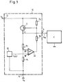
- Fig. 1 shows a known control circuit 10 which from an external supply voltage V b generates an internal operating voltage V ib and maintains the latter substantially constant at an adjustable value.
- a control circuit of this type is described for example in "Halbleitertechnik” by U. Tietze and Ch. Schenk, Springer Verlag, 8th edition, 1986, p. 524, 525.
- the control circuit 10 comprises a terminal 12 for applying the external supply voltage V b and an output A.
- a further terminal 14 is connected to ground V o .
- An operational amplifier OP is connected with its non-inverting input 18 to a highly exact reference voltage source 16 having a reference voltage V ref .
- the reference voltage V ref is consequently present at the non-inverting input 18.
- the inverting input 20 of the operational amplifier OP is connected to a voltage divider R1, R3. Via the resistor R1 the inverting input 20 is connected on the one hand to the terminal 14 connected to ground and on the other via the resistor R3 to the collector of a pnp transistor Q.
- the emitter of the transistor Q is connected to the terminal connected to the supply voltage V b .
- the base of the transistor Q is connected to a further divider R5, R6.
- the one resistor R5 leads to the output terminal 22 of the operational amplifier OP and the other resistor R6 leads to the terminal 12 connected to the supply voltage V b .
- the internal operating voltage V ib to be generated by this circuit is tapped from the collector of the transistor Q and can be supplied via the output A to a digital circuit C.
- the internal operating voltage V ib present at the output A is kept constant by the circuit described above.
- the value of the operating voltage V ib depends on the reference voltage V ref and the values of the resistors R1 and R3.
- the circuit of Fig. 1 functions in detail as follows: In the rest state, i.e. with invariable supply voltage V b , the control circuit described generates, as mentioned above, the internal operating voltage V ib at the output A with a value dependent on the value of the reference voltage V ref and the value of the resistors R1 and R3. The control circuit continuously attempts to reduce the difference between the voltages at the two inputs 18 and 20 of the operational amplifier 22 to zero.
- the operational amplifier OP generates at its output 22 a current which at the connection point of the two resistors R5 and R6 produces a voltage drop which as base voltage drives the transistor Q in such a manner that the collector I c thereof generates at the connection point of the resistors R1 and R3 a voltage which is equal to the reference voltage V ref .
- V ref the supply voltage
- V b rises this results in a rise of the collector current I c of the transistor Q as well so that at the inverting input 20 of the operational amplifier OP a voltage is set which is greater than the reference voltage V ref . Consequently, between the inputs 18 and 20 of the operational amplifier OP a voltage difference is present which leads to a change in the output current at the output 22.
- This modified output current leads to a change of the base bias of the transistor Q1 such that the collector current I c thereof becomes smaller until finally the voltage drop at the inverting input 20 of the operational amplifier OP again assumes the value of the reference voltage V ref .
- the rise of the internal operating voltage V ib is countered by the control circuit 10 through a rise of the supply voltage V b .
- the control circuit 10 achieves the desired effect, i.e. of keeping the internal operating voltage V ib constant at a value fixed by the reference voltage V ref and the resistors R1 and R3.
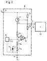
- Fig. 2 shows a circuit arrangement in which by subsequent regulation of the internal operating voltage the influence of the ambient temperature on the switching time is largely eliminated.
- This circuit arrangement corresponds substantially to the circuit arrangement of Fig. 1 and consequently the same reference numerals are used for corresponding components and circuit parts.
- a diode D serving as temperature sensor is inserted parallel to a first part R 1a of the resistor R1 divided into two parts R 1a and R 1b , said first part R 1a of the resistor R1 and the diode D each being connected on one side to ground.
- the temperature behaviour of the diode D and in particular of the diode voltage U AK is exactly known. With increasing temperature this diode voltage U AK decreases by 2 mV/°C. This effect leads on a temperature change to a change in the current flowing through the resistor R1 and thus to a change of the voltage at the inverted input 20 of the operational amplifier OP.
- the circuit arrangement of Fig. 3 differs from the circuit arrangement of Fig. 1 in that the resistor R3 is divided into two resistor parts R 3a and R 3b and that the source-drain path of a P-channel field-effect transistor P and the source-drain path of an N-channel field-effect transistor N are connected in parallel with the resistor part R 3b .
- the gate electrode of the P-channel field-effect transistor is connected to ground and the gate electrode of the N-channel transistor N is connected to the collector of the transistor Q and thus to the output A which furnishes the internally generated operating voltage V ib . Both field-effect transistors are connected in this circuit as current source.
- the two field-effect transistors are employed as reference components for corresponding field-effect transistors in the digital circuit C. Since they are made by the same fabrication process as the corresponding field-effect transistors in the digital circuit C, they are also subject to the same spreads of the fabrication process. These spreads lead inter alia to different channel lengths of the field-effect transistors which in turn influence the switching time of the digital circuit made. As will be apparent below from the description of the function of the circuit arrangement of Fig. 3, the two field-effect transistors P and N are inserted into the control circuit in such a manner that the changes of the switching time due to the spreads of the fabrication process are compensated by a corresponding change in the internal operating voltage V ib generated by the control circuit.
- Fig. 4 a circuit arrangement is illustrated in which the possibilities of influencing the internal operating voltage V ib according to the circuit arrangements of Figs. 2 and 3 are combined. This means that when using the circuit arrangement of Fig. 4 switching times with narrow tolerances can be maintained even with relatively large temperature fluctuations and relatively large spreads of the fabrication process so that the yield in the fabrication of integrated circuits or use in highspeed microprocessor systems can be considerably increased.
- the same reference numerals are used as in the circuit arrangements of Figs. 2 and 3 so that a detailed description of said circuit arrangement would be superfluous.
Landscapes
- Engineering & Computer Science (AREA)
- Physics & Mathematics (AREA)
- Electromagnetism (AREA)
- General Physics & Mathematics (AREA)
- Radar, Positioning & Navigation (AREA)
- Automation & Control Theory (AREA)
- Logic Circuits (AREA)
- Semiconductor Integrated Circuits (AREA)
- Metal-Oxide And Bipolar Metal-Oxide Semiconductor Integrated Circuits (AREA)
- Electronic Switches (AREA)
- Continuous-Control Power Sources That Use Transistors (AREA)
Applications Claiming Priority (2)
| Application Number | Priority Date | Filing Date | Title |
|---|---|---|---|
| DE4137730A DE4137730C2 (de) | 1991-11-15 | 1991-11-15 | In einer Halbleiterschaltung integrierte Schaltungsanordnung |
| DE4137730U | 1991-11-15 |
Publications (3)
| Publication Number | Publication Date |
|---|---|
| EP0542225A2 true EP0542225A2 (de) | 1993-05-19 |
| EP0542225A3 EP0542225A3 (en) | 1993-09-22 |
| EP0542225B1 EP0542225B1 (de) | 1997-04-02 |
Family
ID=6444941
Family Applications (1)
| Application Number | Title | Priority Date | Filing Date |
|---|---|---|---|
| EP92119280A Expired - Lifetime EP0542225B1 (de) | 1991-11-15 | 1992-11-11 | Spannungsregler |
Country Status (4)
| Country | Link |
|---|---|
| US (1) | US5488288A (de) |
| EP (1) | EP0542225B1 (de) |
| JP (1) | JP3269676B2 (de) |
| DE (2) | DE4137730C2 (de) |
Cited By (3)
| Publication number | Priority date | Publication date | Assignee | Title |
|---|---|---|---|---|
| EP0644642A3 (de) * | 1993-07-30 | 1995-05-24 | Texas Instruments Inc | Stromversorgung. |
| US6376207B1 (en) | 1996-03-04 | 2002-04-23 | Scios, Inc. | Assay and reagents for quantifying hBNp |
| EP1010245A4 (de) * | 1997-07-31 | 2004-03-31 | Credence Systems Corp | System zum ausgleichen der temperaturbedingten verzögerungsänderung in einer integrierten schaltung |
Families Citing this family (8)
| Publication number | Priority date | Publication date | Assignee | Title |
|---|---|---|---|---|
| US5723974A (en) * | 1995-11-21 | 1998-03-03 | Elantec Semiconductor, Inc. | Monolithic power converter with a power switch as a current sensing element |
| US5832284A (en) * | 1996-12-23 | 1998-11-03 | International Business Machines Corporation | Self regulating temperature/performance/voltage scheme for micros (X86) |
| US6592985B2 (en) * | 2000-09-20 | 2003-07-15 | Camco International (Uk) Limited | Polycrystalline diamond partially depleted of catalyzing material |
| TWI227961B (en) * | 2003-11-18 | 2005-02-11 | Airoha Tech Corp | Voltage supplying apparatus |
| DE102004004775B4 (de) * | 2004-01-30 | 2006-11-23 | Infineon Technologies Ag | Spannungsregelsystem |
| JP4993092B2 (ja) * | 2007-05-31 | 2012-08-08 | 富士電機株式会社 | レベルシフト回路および半導体装置 |
| JP4990049B2 (ja) * | 2007-07-02 | 2012-08-01 | 株式会社リコー | 温度検出回路 |
| US9285813B2 (en) * | 2014-05-20 | 2016-03-15 | Freescale Semiconductor, Inc. | Supply voltage regulation with temperature scaling |
Family Cites Families (9)
| Publication number | Priority date | Publication date | Assignee | Title |
|---|---|---|---|---|
| NL7907161A (nl) * | 1978-09-27 | 1980-03-31 | Analog Devices Inc | Geintegreerde temperatuurgecompenseerde spannings- referentie. |
| JPS55135780A (en) * | 1979-04-10 | 1980-10-22 | Citizen Watch Co Ltd | Electronic watch |
| US4346343A (en) * | 1980-05-16 | 1982-08-24 | International Business Machines Corporation | Power control means for eliminating circuit to circuit delay differences and providing a desired circuit delay |
| JPS60195625A (ja) * | 1984-03-16 | 1985-10-04 | Hitachi Ltd | 電源制御方式 |
| JP2592234B2 (ja) * | 1985-08-16 | 1997-03-19 | 富士通株式会社 | 半導体装置 |
| US4717836A (en) * | 1986-02-04 | 1988-01-05 | Burr-Brown Corporation | CMOS input level shifting circuit with temperature-compensating n-channel field effect transistor structure |
| US4897613A (en) * | 1988-10-27 | 1990-01-30 | Grumman Corporation | Temperature-compensated circuit for GaAs ECL output buffer |
| US5283762A (en) * | 1990-05-09 | 1994-02-01 | Mitsubishi Denki Kabushiki Kaisha | Semiconductor device containing voltage converting circuit and operating method thereof |
| US5258703A (en) * | 1992-08-03 | 1993-11-02 | Motorola, Inc. | Temperature compensated voltage regulator having beta compensation |
-
1991
- 1991-11-15 DE DE4137730A patent/DE4137730C2/de not_active Expired - Fee Related
-
1992
- 1992-11-11 EP EP92119280A patent/EP0542225B1/de not_active Expired - Lifetime
- 1992-11-11 DE DE69218725T patent/DE69218725T2/de not_active Expired - Fee Related
- 1992-11-12 US US07/974,869 patent/US5488288A/en not_active Expired - Lifetime
- 1992-11-13 JP JP30376992A patent/JP3269676B2/ja not_active Expired - Lifetime
Cited By (3)
| Publication number | Priority date | Publication date | Assignee | Title |
|---|---|---|---|---|
| EP0644642A3 (de) * | 1993-07-30 | 1995-05-24 | Texas Instruments Inc | Stromversorgung. |
| US6376207B1 (en) | 1996-03-04 | 2002-04-23 | Scios, Inc. | Assay and reagents for quantifying hBNp |
| EP1010245A4 (de) * | 1997-07-31 | 2004-03-31 | Credence Systems Corp | System zum ausgleichen der temperaturbedingten verzögerungsänderung in einer integrierten schaltung |
Also Published As
| Publication number | Publication date |
|---|---|
| US5488288A (en) | 1996-01-30 |
| EP0542225A3 (en) | 1993-09-22 |
| EP0542225B1 (de) | 1997-04-02 |
| JP3269676B2 (ja) | 2002-03-25 |
| DE4137730C2 (de) | 1993-10-21 |
| DE4137730A1 (de) | 1993-05-19 |
| JPH06112789A (ja) | 1994-04-22 |
| DE69218725T2 (de) | 1997-10-23 |
| DE69218725D1 (de) | 1997-05-07 |
Similar Documents
| Publication | Publication Date | Title |
|---|---|---|
| EP0573240B1 (de) | Referenz Spannungsgenerator | |
| US5394026A (en) | Substrate bias generating circuit | |
| US6101118A (en) | Voltage regulator for single feed voltage memory circuits, and flash type memory in particular | |
| US6992533B2 (en) | Temperature-stabilized oscillator circuit | |
| US6329871B2 (en) | Reference voltage generation circuit using source followers | |
| CN112698681B (zh) | 一种用于调节电压的电路 | |
| US4264873A (en) | Differential amplification circuit | |
| US6057727A (en) | Accurate constant current generator | |
| US20090295479A1 (en) | Amplifier and offset regulating circuit | |
| EP0542225A2 (de) | Spannungsregler | |
| JPH09171415A (ja) | Cmos電流源回路 | |
| CN112711288B (zh) | 具有温度变化补偿的电压参考产生 | |
| US11809207B2 (en) | Temperature compensation circuit and semiconductor integrated circuit using the same | |
| US5045773A (en) | Current source circuit with constant output | |
| CN114296503B (zh) | 一种超低功耗可编程低压差线性稳压源电路 | |
| US4587478A (en) | Temperature-compensated current source having current and voltage stabilizing circuits | |
| US6940338B2 (en) | Semiconductor integrated circuit | |
| JP2590378B2 (ja) | 論理回路 | |
| US5541539A (en) | Digital current switch | |
| US4325019A (en) | Current stabilizer | |
| US6198343B1 (en) | Current mirror circuit | |
| KR0156232B1 (ko) | 주파수 보상회로 | |
| US4871931A (en) | Logic circuit resistant to errors due to supply fluctuations | |
| US4577119A (en) | Trimless bandgap reference voltage generator | |
| US5748030A (en) | Bias generator providing process and temperature invariant MOSFET transconductance |
Legal Events
| Date | Code | Title | Description |
|---|---|---|---|
| PUAI | Public reference made under article 153(3) epc to a published international application that has entered the european phase |
Free format text: ORIGINAL CODE: 0009012 |
|
| AK | Designated contracting states |
Kind code of ref document: A2 Designated state(s): DE FR GB IT NL |
|
| PUAL | Search report despatched |
Free format text: ORIGINAL CODE: 0009013 |
|
| AK | Designated contracting states |
Kind code of ref document: A3 Designated state(s): DE FR GB IT NL |
|
| 17P | Request for examination filed |
Effective date: 19940321 |
|
| 17Q | First examination report despatched |
Effective date: 19950222 |
|
| GRAG | Despatch of communication of intention to grant |
Free format text: ORIGINAL CODE: EPIDOS AGRA |
|
| GRAH | Despatch of communication of intention to grant a patent |
Free format text: ORIGINAL CODE: EPIDOS IGRA |
|
| GRAH | Despatch of communication of intention to grant a patent |
Free format text: ORIGINAL CODE: EPIDOS IGRA |
|
| GRAH | Despatch of communication of intention to grant a patent |
Free format text: ORIGINAL CODE: EPIDOS IGRA |
|
| GRAA | (expected) grant |
Free format text: ORIGINAL CODE: 0009210 |
|
| AK | Designated contracting states |
Kind code of ref document: B1 Designated state(s): DE FR GB IT NL |
|
| PG25 | Lapsed in a contracting state [announced via postgrant information from national office to epo] |
Ref country code: NL Effective date: 19970402 |
|
| REF | Corresponds to: |
Ref document number: 69218725 Country of ref document: DE Date of ref document: 19970507 |
|
| ET | Fr: translation filed | ||
| NLV1 | Nl: lapsed or annulled due to failure to fulfill the requirements of art. 29p and 29m of the patents act | ||
| PLBE | No opposition filed within time limit |
Free format text: ORIGINAL CODE: 0009261 |
|
| STAA | Information on the status of an ep patent application or granted ep patent |
Free format text: STATUS: NO OPPOSITION FILED WITHIN TIME LIMIT |
|
| 26N | No opposition filed | ||
| REG | Reference to a national code |
Ref country code: GB Ref legal event code: IF02 |
|
| PGFP | Annual fee paid to national office [announced via postgrant information from national office to epo] |
Ref country code: DE Payment date: 20041221 Year of fee payment: 13 |
|
| PG25 | Lapsed in a contracting state [announced via postgrant information from national office to epo] |
Ref country code: DE Free format text: LAPSE BECAUSE OF NON-PAYMENT OF DUE FEES Effective date: 20060601 |
|
| PGFP | Annual fee paid to national office [announced via postgrant information from national office to epo] |
Ref country code: IT Payment date: 20061130 Year of fee payment: 15 |
|
| PGFP | Annual fee paid to national office [announced via postgrant information from national office to epo] |
Ref country code: FR Payment date: 20071105 Year of fee payment: 16 Ref country code: GB Payment date: 20071005 Year of fee payment: 16 |
|
| GBPC | Gb: european patent ceased through non-payment of renewal fee |
Effective date: 20081111 |
|
| PG25 | Lapsed in a contracting state [announced via postgrant information from national office to epo] |
Ref country code: IT Free format text: LAPSE BECAUSE OF NON-PAYMENT OF DUE FEES Effective date: 20071111 |
|
| REG | Reference to a national code |
Ref country code: FR Ref legal event code: ST Effective date: 20090731 |
|
| PG25 | Lapsed in a contracting state [announced via postgrant information from national office to epo] |
Ref country code: GB Free format text: LAPSE BECAUSE OF NON-PAYMENT OF DUE FEES Effective date: 20081111 |
|
| PG25 | Lapsed in a contracting state [announced via postgrant information from national office to epo] |
Ref country code: FR Free format text: LAPSE BECAUSE OF NON-PAYMENT OF DUE FEES Effective date: 20081130 |