EP0542307A2 - Dispositif d'affichage d'images et méthode de commande pour ce dispositif - Google Patents
Dispositif d'affichage d'images et méthode de commande pour ce dispositif Download PDFInfo
- Publication number
- EP0542307A2 EP0542307A2 EP92119484A EP92119484A EP0542307A2 EP 0542307 A2 EP0542307 A2 EP 0542307A2 EP 92119484 A EP92119484 A EP 92119484A EP 92119484 A EP92119484 A EP 92119484A EP 0542307 A2 EP0542307 A2 EP 0542307A2
- Authority
- EP
- European Patent Office
- Prior art keywords
- voltage
- noise
- driving
- reference voltage
- driving means
- Prior art date
- Legal status (The legal status is an assumption and is not a legal conclusion. Google has not performed a legal analysis and makes no representation as to the accuracy of the status listed.)
- Granted
Links
Images


Classifications
-
- G—PHYSICS
- G09—EDUCATION; CRYPTOGRAPHY; DISPLAY; ADVERTISING; SEALS
- G09G—ARRANGEMENTS OR CIRCUITS FOR CONTROL OF INDICATING DEVICES USING STATIC MEANS TO PRESENT VARIABLE INFORMATION
- G09G3/00—Control arrangements or circuits, of interest only in connection with visual indicators other than cathode-ray tubes
- G09G3/20—Control arrangements or circuits, of interest only in connection with visual indicators other than cathode-ray tubes for presentation of an assembly of a number of characters, e.g. a page, by composing the assembly by combination of individual elements arranged in a matrix no fixed position being assigned to or needed to be assigned to the individual characters or partial characters
- G09G3/34—Control arrangements or circuits, of interest only in connection with visual indicators other than cathode-ray tubes for presentation of an assembly of a number of characters, e.g. a page, by composing the assembly by combination of individual elements arranged in a matrix no fixed position being assigned to or needed to be assigned to the individual characters or partial characters by control of light from an independent source
- G09G3/36—Control arrangements or circuits, of interest only in connection with visual indicators other than cathode-ray tubes for presentation of an assembly of a number of characters, e.g. a page, by composing the assembly by combination of individual elements arranged in a matrix no fixed position being assigned to or needed to be assigned to the individual characters or partial characters by control of light from an independent source using liquid crystals
- G09G3/3611—Control of matrices with row and column drivers
- G09G3/3696—Generation of voltages supplied to electrode drivers
-
- G—PHYSICS
- G09—EDUCATION; CRYPTOGRAPHY; DISPLAY; ADVERTISING; SEALS
- G09G—ARRANGEMENTS OR CIRCUITS FOR CONTROL OF INDICATING DEVICES USING STATIC MEANS TO PRESENT VARIABLE INFORMATION
- G09G3/00—Control arrangements or circuits, of interest only in connection with visual indicators other than cathode-ray tubes
- G09G3/20—Control arrangements or circuits, of interest only in connection with visual indicators other than cathode-ray tubes for presentation of an assembly of a number of characters, e.g. a page, by composing the assembly by combination of individual elements arranged in a matrix no fixed position being assigned to or needed to be assigned to the individual characters or partial characters
- G09G3/34—Control arrangements or circuits, of interest only in connection with visual indicators other than cathode-ray tubes for presentation of an assembly of a number of characters, e.g. a page, by composing the assembly by combination of individual elements arranged in a matrix no fixed position being assigned to or needed to be assigned to the individual characters or partial characters by control of light from an independent source
- G09G3/36—Control arrangements or circuits, of interest only in connection with visual indicators other than cathode-ray tubes for presentation of an assembly of a number of characters, e.g. a page, by composing the assembly by combination of individual elements arranged in a matrix no fixed position being assigned to or needed to be assigned to the individual characters or partial characters by control of light from an independent source using liquid crystals
- G09G3/3611—Control of matrices with row and column drivers
-
- G—PHYSICS
- G09—EDUCATION; CRYPTOGRAPHY; DISPLAY; ADVERTISING; SEALS
- G09G—ARRANGEMENTS OR CIRCUITS FOR CONTROL OF INDICATING DEVICES USING STATIC MEANS TO PRESENT VARIABLE INFORMATION
- G09G2300/00—Aspects of the constitution of display devices
- G09G2300/04—Structural and physical details of display devices
- G09G2300/0421—Structural details of the set of electrodes
- G09G2300/043—Compensation electrodes or other additional electrodes in matrix displays related to distortions or compensation signals, e.g. for modifying TFT threshold voltage in column driver
-
- G—PHYSICS
- G09—EDUCATION; CRYPTOGRAPHY; DISPLAY; ADVERTISING; SEALS
- G09G—ARRANGEMENTS OR CIRCUITS FOR CONTROL OF INDICATING DEVICES USING STATIC MEANS TO PRESENT VARIABLE INFORMATION
- G09G2320/00—Control of display operating conditions
- G09G2320/02—Improving the quality of display appearance
- G09G2320/0209—Crosstalk reduction, i.e. to reduce direct or indirect influences of signals directed to a certain pixel of the displayed image on other pixels of said image, inclusive of influences affecting pixels in different frames or fields or sub-images which constitute a same image, e.g. left and right images of a stereoscopic display
-
- G—PHYSICS
- G09—EDUCATION; CRYPTOGRAPHY; DISPLAY; ADVERTISING; SEALS
- G09G—ARRANGEMENTS OR CIRCUITS FOR CONTROL OF INDICATING DEVICES USING STATIC MEANS TO PRESENT VARIABLE INFORMATION
- G09G2330/00—Aspects of power supply; Aspects of display protection and defect management
- G09G2330/02—Details of power systems and of start or stop of display operation
Definitions
- the present invention relates to an image display device and a method of driving the same, particularly to a matrix-type liquid crystal display device performing a multiplex driving.
- a multiplex driving of a time division driving system employing a matrix electrode is performed.
- a pair of electrode substrates are opposingly arranged, a plurality of strip - like row electrodes (X - electrode) are parallely arranged on a first substrate, a plurality of strip - like column electrodes (Y - electrode) are parallely arranged on an opposing second substrate, which are orthogonal to the row electrodes, and a liquid crystal is enclosed and interposed between the both electrode substrates.
- a signal of a row electrode waveform composed of a selecting voltage and a non - selecting voltage is applied on the row electrode in a predetermined frame period, in synchronism therewith, a signal of a column electrode waveform composed of an ON - voltage and an OFF - voltage is supplied on the column electrode and a successive line scanning is performed, thereby performing the display by exciting voltages at liquid crystals at desired matrix intersection point positions (pixel position).
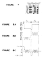
- FIG. 7 shows a display state of a liquid crystal panel to he displayed by these driving waveforms.
- a liquid crystal panel having a 7 x 7 dots construction is shown.
- the display dot in a hatched portion indicates an ON-state (switch on state), whereas the display dot at a white portion, an OFF - state (switch off state).
- the ON - voltage or the OFF-voltage is applied on the respective column electrodes S1 through S7. That is to say, when a dot at an intersection point of a certain row electrode and a certain column electrode, is to be switched on, the ON - voltage is applied on the column electrode when the row electrode is in a selected state, whereas, when it is not to be switched on, the OFF-voltage is applied thereon when the row electrode is in a selected state.
- Figure 8A shows a driving waveform applied on the row electrode C1, Figure 8B, a driving waveform applied on the column electrode S2, and Figure 8C, a driving waveform applied on a dot at the intersection point of the row electrode C1 and the column electrode S2.
- Figure 9A shows a driving waveform applied on the row electrode C2, Figure 9B, a driving waveform applied on the column electrode S5, and Figure 9C, a driving waveform applied on a dot at the intersection point of the row electrode C2 and the column electrode S5.
- F1 and F2 designate frame periods.
- V5 designates a selecting voltage, V1, a non - selecting voltage, V0, an ON - voltage and V2, an OFF - voltage.
- V0 designates a selecting voltage, V4, a non - selecting voltage, V5, an ON-voltage and V3, an OFF-voltage.
- This driving method is called Optimized Amplitude Selective addressing method which has conven - tionally been performed.
- FIG 10 shows a conventional example of a method of supplying the respective voltages of V0, V1, V2, V3, V4 and V5.
- V0 and V5 are supplied by a power supply source or an emitter follower employing a transistor.
- a display capacity of the liquid crystal is comparatively small, as shown in an example of Figure 10A, they are directly supplied to driver ICs from divided resistors.
- the display capacity thereof is comparatively large, as shown in an example of Figure 10B, they are inputted to predetermined terminals of the respective driver ICs whereby impedances thereof are lowered by inserting voltage followers employing operational amplifiers after the divided resistors.
- the driver IC is a driving means having a function whereby a row electrode waveform composed of a selecting voltage and a non-selecting voltage, is applied on a row electrode of a matrix-type display device, and a column electrode waveform composed of an ON - voltage and an OFF - voltage, is controlled and applied on a column electrode.
- V adj designates a control voltage which is supplied for controlling the liquid crystal display panel to be provided with a brightness which is easy to see.
- an image display device having an electro - optical medium interposed between a pair of electrode substrates composing a matrix electrode, a driving means for driving said electro - optical medium by selectively applying a voltage on said matrix electrode and a reference voltage generator for supplying said driving means with a predetermined driving voltage, characterized by that
- a noise compensating means is interposed between the driving means and said reference voltage generator
- said noise compensating means detecting a noise in a voltage supplied from the reference voltage generator to the electro-optical medium at a predetermined noise detecting position, forming a noise compensating voltage having a first polarity reverse to a second polarity of said noise by using the noise, and supplying said noise compensating voltage to the driving means.
- the image display device according to the first aspect, wherein the noise detecting position is at an input portion of the driving means for supplying the voltage.
- the image display device according to the first aspect, wherein a dummy electrode is provided on the electrode substrate and the noise detecting position is provided at said dummy electrode.
- the noise compensating means is provided with an integrator, a change - over switch and an ON - OFF switch,
- a first input terminal of the integrator being connected to the predetermined noise detecting position through the ON - OFF switch, a second input terminal of the integrator being supplied with the reference voltage generated by the reference voltage generator as an offset voltage.
- the driving means is supplied with an output of the reference voltage generator and a noise compensating voltage which is obtained by amplifying a difference between an input voltage at an input terminal of the driving means for a supply voltage and the reference voltage and by performing a negative feedback.
- the noise compensating means is composed of a first differential amplifying means and a second differential amplifying means
- a positive input terminal of said first differential amplifying means being inputted with an output of the reference voltage generator, an output terminal thereof being connected to an input terminal of the driving means for a supply voltage, a negative input terminal thereof being inputted with an output of said second differential amplifying means whereby a difference between the reference voltage and a voltage at the input terminal of the driving means for the supply voltage is amplified.
- the noise compensating means is composed of a delay means, an inverting amplifier and a change-over switch,
- the applicant already proposed a method of driving as a method of driving a liquid crystal display element employing a fast-responsing liquid crystal, wherein the "relaxation phenomena" of a liquid crystal is restrained by simultaneously selecting a plurality of row electrodes, and lowering of the contrast ratio thereof is restrained.
- a method of driving as a method of driving a liquid crystal display element employing a fast-responsing liquid crystal, wherein the "relaxation phenomena" of a liquid crystal is restrained by simultaneously selecting a plurality of row electrodes, and lowering of the contrast ratio thereof is restrained.
- This method is basically a method of driving a fast-responsing liquid crystal wherein row electrodes of matrix liquid crystal display elements composed of a plurality of row electrodes and a plurality of column electrodes, are divided into a plurality of row electrode subgroups respectively including a plurality of row electrodes, and the row electrode subgroup is selected as a selecting unit.
- a row electrode unit is selected, as a selecting voltage, a voltage which is divided into a plurality of stages and provided with an amplitude of V, (V r >0) in the positive or the negative direction with respect to an intermediate voltage. Furthermore, when it is not selected, the intermediate voltage is applied thereon as a non-selecting voltage.
- a time interval from when a voltage corresponding to a stage among the selecting voltages is applied thereon to when a voltage corresponding to the next stage is applied thereon, is selected so that an orientation of liquid crystal molecules generated by the voltage application corresponding to a single stage among the selecting voltages, is substantially maintained until the voltage application corresponding to the next stage.
- the following driving method is adopted.
- J x L (J is an integer of 1 or more and L is an integer of 2 or more) of row electrodes are divided into J of row electrode subgroups respectively composed of L of row electrodes, the selecting voltage is applied in the following sequence.
- the image device of this invention is applicable to the image display device wherein such a driving method is adopted, and the effect is considerable.
- various levels of voltages are applied on the row electrodes and column electrodes.
- Noise compensating circuits of this invention are to be connected to outputs of a reference voltage generator corresponding with either one of the levels of the voltages.
- a reference voltage generator for outputting a reference voltage employed in driving a matrix-type display body, with respect to the above-mentioned V0 and V5, they are supplied directly from a power source or by emitter followers in use of transistors, and with respect to V1 through V4, they are supplied from the resistor-dividing of the power source.
- a noise compensating means is connected to the output side of the reference voltage generator.
- the reference voltage a selecting voltage, a non - selecting voltage, an ON - voltage, an OFF - voltage or the like is pointed out. It is necessary to connect the noise compensating means to an output of at least one of those reference voltages.
- a liquid crystal panel is constructed by interposing a dielectric body called a liquid crystal between transference electrodes, which is a capacitative load in view of a driving side thereof. Furthermore, a resistance value of the transference electrodes is not zero and is provided with a limited value. Therefore, even if an ideal waveform is applied thereon from a driver IC, the waveform is considerably distorted inside of the liquid crystal panel, thereby causing a nonuniformity of display.
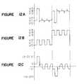
- An example of the nonuniformity of the display will be explained by using Figures 11 A and 11 B, Figures 12A through 12C, Figures 13A through 13C and Figure 14. In this display, a so-called positive display wherein the more the root mean square voltage applied on a dot, the darker the dot.
- the voltage waveform at the dot portions of the row electrode C2 is shown in Figure 13A, the voltage waveform at dot portions of the column electrode S7, in Figure 13B and the waveform applied on a dot at the intersection point of the row electrode C2 and the column electrode S7, in Figure 13C.
- Figure 13A spike - like voltage distortions are generated at the non - selecting voltage level of the row electrode waveform. Accordingly, distortions are generated in the waveform at the non - selecting time as shown in Figure 13C.
- the amplitude of the detected waveform is attenuated by the influences of the resistance of the electrode and an output impedance of a driver IC, compared with that of a waveform of a voltage actually applied on the liquid crystal. Therefore, the spike - like voltage distortion is generated on the non - selecting voltage level of the row electrode waveform.
- This invention can reduce the nonuniformity of display by an original construction wherein a voltage distortion of a driving waveform generated inside of a panel in figures or letters which an image display device displays, is detected by at least one of a selecting voltage supplied to a driver IC, a non - selecting voltage, an ON - voltage and an OFF - voltage, the noise is converted into a noise compensating voltage having a polarity which is reverse to that of the noise, and the noise compensating voltage is applied to the driving means.
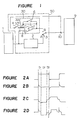
- Figure 1 shows a circuit construction of an important part of a first embodiment of a liquid crystal display device according to the present invention.
- Figures 2A through 2D show time charts of voltage waveforms at respective points when the circuit is operated.
- Figure 2A designates a waveform to be applied to a column electrode
- Figure 2B a voltage distortion generated at an input terminal 10 of a driver IC 9 when a noise compensating means is not employed
- Figure 2C an output waveform of an integrator 30, and Figure 2D, an example of a voltage waveform at the non-selecting voltage input terminal 10 when the noise compensating means is employed.
- Figures 2B through 2D voltage components deviated from a reference voltage are shown.
- a reference numeral 50 designates a noise compensating means, 1, a reference voltage generator for generating one of two non - selecting voltages, and 9, a driver IC as a driving means.
- the driver IC 9 is connected to a matrix electrode for driving a liquid crystal, not shown, which selectively apply a voltage, for instance, on a row electrode.
- the noise compensating means 50 is mainly composed of the integrator 30, a change-over switch 3 and an ON - OFF switch 4.
- An output terminal of the change-over switch 3 is connected to an input terminal of a non - selecting voltage 10 of the driver IC 9, a first switching terminal A on the input side thereof is connected to an output terminal of the reference voltage generator 1, and a second switching terminal B at the input side thereof is connected to an output terminal of the integrator 30.
- the switching terminal A of the change-over switch 3 may be connected to the output terminal of the reference voltage generator 1 through a buffer amplifier 2 of an operational amplifier or the like provided as a voltage follower wherein the impedance of the reference voltage is lowered, according to the necessities.
- the voltage to be supplied to the driver IC 9 may be switched to either one of the output voltage of the integrator 30 and the output voltage of the reference voltage generator 1.
- the integrator 30 is composed of an operational amplifier 5, a capacitor 7 and a discharge switch 6 in this example. Therefore, when the discharge switch 6 is opened, the integrator 30 functions, whereas, when the discharged switch 6 is closed, the integrator 30 is discharged and reset.
- the input terminal 10 of the driver IC 9 is connected to a negative input terminal 32 of the operational amplifier 5 through the ON - OFF switch 4. Therefore, when the ON - OFF switch 4 is closed while the discharge switch 6 is open, a noise voltage signal of which polarity is inverted, is integrated by the integrator 30.
- a positive input terminal 8 of the operational amplifier 5 is connected to a predetermined output terminal of the reference voltage generator 1 and is inputted with a reference voltage for controlling an offset voltage.
- the column electrode waveform is the one shown in Figure 2A.
- a spike - like voltage distortion (noise) as shown in Figure 2B is generated at the non - selecting voltage input terminal 10 of the driver IC 9.
- This noise compensating voltage is a voltage having a polarity inverse to that of the spike - like noise.
- a voltage control is performed while looking at the display, until the nonuniformity of display is extinguished.
- This voltage can be changed by changing an input resistance 33 provided at the input side of the integrator 30 of which gain may be changed by providing an amplifier thereafter.
- the correction can be performed by providing the amplifier with a corresponding nonlinearity.
- Figure 2D designates a voltage waveform at the non-selecting voltage input terminal 10 when the change-over switch 3 is connected to B during time periods of t 2 and b.
- a standby period t 4 is provided after the reset period 1 3 , and a sequence composed of the noise sampling period, the hold period, the reset period and the standby period is iterated.
- the change-over switch 3 is connected to the terminal A.
- the ON - OFF switch 4 remains open.
- the discharge switch 6 may be open or closed.
- a buffer amplifier may be interposed between the noise compensating means and the driving means according to the necessity. In this way, even when the capacity of the liquid crystal varies considerably, the compensating means sufficiently works.
- FIG. 3 shows a circuit construction of another embodiment of a liquid crystal display device of this invention employing a similar circuit construction.
- the output side of the driver IC 9 is connected to terminals of respective row electrodes of a liquid crystal panel 11, whereas the output side of a driver IC 12 for driving column electrodes is connected to terminals of respective column electrodes of the liquid crystal panel 11.
- the negative input terminal of the operational amplifier 5 in the integrator 30 is connected to a dummy electrode of a liquid crystal panel for detecting the spike-noise through a buffer amplifier 14 and the ON - OFF switch 4.
- the circuit of this example differs from the embodiment in Figure 1 in the detecting method (detecting position) of the spike - like noise and the other construction and operation are the same with those in the embodiment of Figure 1. Accordingly, the same notation is attached to the same portion with that in Figure 1 and the explanation of operation is omitted. Furthermore, the buffer amplifier 14 may be omitted.
- FIG. 4 shows a second example of a portion of the circuit supplying the reference voltage to the driving means in the image display device of this invention.
- a reference numeral 61 designates divided resistors for generating one of two non -selecting voltages, which is a reference voltage generator.
- a numeral 66 designates a noise compensating means in this invention, and 64, a driver IC (driving means). The noise compensating means 66 is interposed between the reference voltage generator 61 and a driver IC 64.
- the noise compensating means 66 is composed of a first operational amplifier 62 (differential amplifying means) and a second operational amplifier 65 (differential amplifying means).
- the second operational amplifier 65 is employed for amplifying a difference (noise component) between a voltage at an input terminal 63 of a supply voltage of the driver IC 64 and the non - selecting voltage.
- a positive input terminal thereof is connected to the supply voltage input terminal (noise detecting position in this example) of the driver IC 64 and a negative input terminal thereof is inputted with the non - selecting voltage as an offset voltage, which composes an amplifying circuit of the noise.
- the gain a of the second operational amplifier is determined to be 3 in this example. However, a range of 2 to 6 is preferable for the gain.
- the first operational amplifier 62 is employed for providing the voltage supplied to the driver IC 64 with a low impedance.
- the positive input terminal thereof is supplied with the non - selecting voltage outputted from the reference voltage generator 61 and the negative input terminal thereof is connected to the output terminal of the second operational amplifier 65. Furthermore, the output terminal thereof is connected to the input terminal for the supply voltage of the driver IC 64. Accordingly, a noise compensating voltage which is formed by amplifying a difference between a voltage at the input terminal 63 for the supply voltage of the driver IC 64 and the non - selecting voltage and by performing a negative feedback, is applied on the driver IC 64 along with the non - selecting voltage outputted from the reference voltage generator 61.
- the detecting line for performing the negative feedback is preferably to be drawn from a location as near to the load as possible.
- the noise detection is performed at the input terminal for the supply voltage of the driving means.
- the noise detection may be performed by providing a dummy electrode for detecting the noise on the substrates interposing the liquid crystal layer.
- Figure 5 shows the circuit construction of an important part of a third example of a liquid crystal device according to the present invention.
- Figures 6A through 6E show time charts of voltage waveforms when the circuit is operated.
- a reference numeral 78 designates a noise compensating means, 71, divided resistors, which is a reference voltage generator for generating one of two non - selecting voltages, and 77, a driver IC which is a driving means.
- the driver IC 77 is connected to a matrix electrode for driving a liquid crystal, not shown, which selectively applies voltage on, for instance, row electrodes.
- the noise compensating means 78 is mainly composed of a change-over switch 73, a delay means 74 and an inverting amplifier 75.
- An output terminal of the change-over switch 73 is connected to an input terminal 76 for non - selecting voltage of the driver IC 77, a first switching terminal A at the input side thereof is connected to an output terminal of a reference voltage generator 71 and a second switching terminal B at the input side thereof is connected to the output terminal of the reference voltage generator 71 through the delay means 74 and the inverting amplifier 75.
- the respective switching terminals A and B of the change - over switch 73 may be connected to the output terminal of the reference voltage generator 71 through a buffer amplifier 72 of an operational amplifier or the like provided as a voltage follower that provides the reference voltage with a low impedance, as shown in Figure 1, according to the necessity.
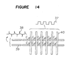
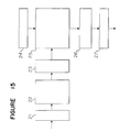
- the delay means 74 may be of a delay line of analogue system such as a CCD delay line, a glass delay line or the like, or a construction shown in Figure 15.
- a reference numeral 21 designates an input buffer amplifier, 22, an A/D converter, 23, a tri-state buffer gate, 24, an address counter of a RAM and a control signal generator, 25, a RAM, 26, a D/A converter and 27, an output buffer amplifier.
- This is a delay line of a digital system wherein A/D-converted data are memorized in a memory, which are read out being delayed for a certain time, and D/A-converted.
- a differential amplifier may be employed as the inverting amplifier 75.
- the position of the delay means 74 and the inverting amplifier 75 may be interchanged in the Figure.
- the column electrode waveform is as shown in Figure 6A.
- a spike - like voltage distortion (noise) as shown in Figure 6B is generated at the input terminal 76 for the non - selecting voltage of the driver IC 77.
- the change-over switch 73 is connected to the switching terminal A during the starting time ti (reference voltage supply period, t 1 ⁇ t) in a cycle of a single row electrode selecting time, and to the switching terminal B during a residual time (noise correcting period) thereof.
- the reference voltage outputted from the reference voltage generator superposed with the noise is applied to the input terminal 76 of the driver IC 77, and during the noise correcting period, a voltage wherein the reference voltages superposed with a voltage provided with a phase reverse to that in the reference voltage supply period, is supplied thereto.
- the spike - like voltage distortion is attenuated compared with a wave height value thereof inside of the liquid crystal panel when it is detected by the delay means 74. Therefore, an amplification is performed in the amplifier 75 to correct the attenuated value.
- the delay means 74 is provided with 6 bits as the bit number in case of a digital system and the sampling frequency is 10 MHz.
- the delay time t depends on the capacity of the liquid crystal panel. In this example, the delay time is set to be 10 asec.
- the reduction of the nonuniformity of display is made possible in this invention, by canceling the voltage distortion which is superposed on the reference voltage supplied to the driver IC which is the driving means, by the effective feedback circuit. Furthermore, since the circuit construction is simple, the invention is provided with an advantage of realizing the circuit at a low cost.
Landscapes
- Engineering & Computer Science (AREA)
- Chemical & Material Sciences (AREA)
- Crystallography & Structural Chemistry (AREA)
- Physics & Mathematics (AREA)
- Computer Hardware Design (AREA)
- General Physics & Mathematics (AREA)
- Theoretical Computer Science (AREA)
- Liquid Crystal Display Device Control (AREA)
Applications Claiming Priority (8)
| Application Number | Priority Date | Filing Date | Title |
|---|---|---|---|
| JP327140/91 | 1991-11-15 | ||
| JP32714091 | 1991-11-15 | ||
| JP35938191A JP3175784B2 (ja) | 1991-11-15 | 1991-12-27 | 画像表示装置 |
| JP03359374A JP3128309B2 (ja) | 1991-12-27 | 1991-12-27 | 画像表示装置およびその駆動方法 |
| JP03359375A JP3121654B2 (ja) | 1991-12-27 | 1991-12-27 | 画像表示装置およびその駆動方法 |
| JP359375/91 | 1991-12-27 | ||
| JP359374/91 | 1991-12-27 | ||
| JP359381/91 | 1991-12-27 |
Publications (3)
| Publication Number | Publication Date |
|---|---|
| EP0542307A2 true EP0542307A2 (fr) | 1993-05-19 |
| EP0542307A3 EP0542307A3 (en) | 1993-08-18 |
| EP0542307B1 EP0542307B1 (fr) | 1997-08-06 |
Family
ID=27480386
Family Applications (1)
| Application Number | Title | Priority Date | Filing Date |
|---|---|---|---|
| EP92119484A Expired - Lifetime EP0542307B1 (fr) | 1991-11-15 | 1992-11-13 | Dispositif d'affichage d'images et méthode de commande pour ce dispositif |
Country Status (3)
| Country | Link |
|---|---|
| US (1) | US5489910A (fr) |
| EP (1) | EP0542307B1 (fr) |
| DE (1) | DE69221434T2 (fr) |
Cited By (8)
| Publication number | Priority date | Publication date | Assignee | Title |
|---|---|---|---|---|
| EP0570001A3 (fr) * | 1992-05-14 | 1994-11-30 | Toshiba Kk | Dispositif d'affichage à cristaux liquides. |
| US5440322A (en) * | 1993-11-12 | 1995-08-08 | In Focus Systems, Inc. | Passive matrix display having reduced image-degrading crosstalk effects |
| EP0731442A3 (fr) * | 1995-03-06 | 1996-10-02 | Thomson Multimedia Sa | |
| US5600345A (en) * | 1995-03-06 | 1997-02-04 | Thomson Consumer Electronics, S.A. | Amplifier with pixel voltage compensation for a display |
| US5771030A (en) * | 1994-01-28 | 1998-06-23 | International Business Machines Corporation | Apparatus and method for driving liquid crystal |
| EP0858065A1 (fr) * | 1997-02-07 | 1998-08-12 | Hitachi, Ltd. | Affichage à cristaux liquides avec fonction de compensation de tension |
| US6252566B1 (en) | 1997-06-05 | 2001-06-26 | Thomson-Lcd | Compensation process for a disturbed capacitive circuit and application to matrix display screens |
| US6919874B1 (en) | 1994-05-17 | 2005-07-19 | Thales Avionics Lcd S.A. | Shift register using M.I.S. transistors and supplementary column |
Families Citing this family (28)
| Publication number | Priority date | Publication date | Assignee | Title |
|---|---|---|---|---|
| EP0727083A1 (fr) * | 1994-09-01 | 1996-08-21 | Koninklijke Philips Electronics N.V. | Panneau d'affichage a cristaux liquides |
| JPH0876093A (ja) * | 1994-09-08 | 1996-03-22 | Texas Instr Japan Ltd | 液晶パネル駆動装置 |
| JP2667373B2 (ja) * | 1994-12-13 | 1997-10-27 | インターナショナル・ビジネス・マシーンズ・コーポレイション | アナログ・ビデオ信号補正装置及びtft液晶表示装置 |
| JPH08286642A (ja) * | 1995-04-11 | 1996-11-01 | Sony Corp | 表示装置 |
| JP3372142B2 (ja) * | 1995-07-10 | 2003-01-27 | 株式会社東芝 | 液晶表示装置及びその駆動回路 |
| US5818402A (en) * | 1996-01-19 | 1998-10-06 | Lg Electronics Inc. | Display driver for reducing crosstalk by detecting current at the common electrode and applying a compensation voltage to the common electrode |
| US6072477A (en) * | 1996-07-10 | 2000-06-06 | Matsushita Electric Industrial Co., Ltd. | El display and driving circuit for the same |
| JP3244630B2 (ja) * | 1996-08-28 | 2002-01-07 | アルプス電気株式会社 | 液晶表示装置の駆動回路 |
| WO1999035521A1 (fr) * | 1998-01-09 | 1999-07-15 | Hitachi, Ltd. | Affichage a cristaux liquides |
| TW504598B (en) * | 1998-03-26 | 2002-10-01 | Toshiba Corp | Flat display apparatus |
| DE69917479T2 (de) * | 1998-10-26 | 2005-06-02 | Janez Pirs | Ansteuerungsschema und elektronischer schaltkreis für ein elektooptisches lcd-schaltelement |
| US20030043139A1 (en) * | 1998-10-31 | 2003-03-06 | David W. Engler | Method and apparatus for automatic digital dc balancing for an imager of a display |
| WO2001059750A1 (fr) * | 2000-02-10 | 2001-08-16 | Hitachi, Ltd. | Afficheur d'images |
| JP3779166B2 (ja) * | 2000-10-27 | 2006-05-24 | シャープ株式会社 | 階調表示用電圧発生装置、及びそれを備えた階調表示装置 |
| JP3533185B2 (ja) * | 2001-01-16 | 2004-05-31 | Necエレクトロニクス株式会社 | 液晶ディスプレイの駆動回路 |
| US6653992B1 (en) * | 2001-02-28 | 2003-11-25 | Varian Medical Systems, Inc. | Method and circuit for reduction of correlated noise |
| JP3647426B2 (ja) * | 2001-07-31 | 2005-05-11 | キヤノン株式会社 | 走査回路及び画像表示装置 |
| US6657609B2 (en) * | 2001-09-28 | 2003-12-02 | Koninklijke Philips Electronics N.V. | Liquid crystal displays with reduced flicker |
| JP3715967B2 (ja) * | 2002-06-26 | 2005-11-16 | キヤノン株式会社 | 駆動装置及び駆動回路及び画像表示装置 |
| US7095028B2 (en) * | 2003-10-15 | 2006-08-22 | Varian Medical Systems | Multi-slice flat panel computed tomography |
| US7589326B2 (en) * | 2003-10-15 | 2009-09-15 | Varian Medical Systems Technologies, Inc. | Systems and methods for image acquisition |
| KR101056373B1 (ko) * | 2004-09-07 | 2011-08-11 | 삼성전자주식회사 | 액정 표시 장치의 아날로그 구동 전압 및 공통 전극 전압발생 장치 및 액정 표시 장치의 아날로그 구동 전압 및공통 전극 전압 제어 방법 |
| JP4241781B2 (ja) * | 2006-08-10 | 2009-03-18 | エプソンイメージングデバイス株式会社 | 電気光学装置、駆動回路および電子機器 |
| KR101258644B1 (ko) * | 2006-09-20 | 2013-04-26 | 삼성전자주식회사 | 시분할 구동 방식을 이용한 소스 드라이버, 이를 포함하는 디스플레이 장치, 및 이의 구동 방법 |
| WO2009011150A1 (fr) * | 2007-07-18 | 2009-01-22 | Sharp Kabushiki Kaisha | Dispositif d'affichage et son procédé de commande |
| JP6633346B2 (ja) * | 2014-10-31 | 2020-01-22 | 株式会社半導体エネルギー研究所 | 表示装置 |
| CN105845096B (zh) * | 2016-06-03 | 2018-07-20 | 京东方科技集团股份有限公司 | 面板驱动装置以及显示装置 |
| CN109164862A (zh) * | 2018-07-24 | 2019-01-08 | 惠科股份有限公司 | 一种基准电压产生系统和产生方法 |
Family Cites Families (10)
| Publication number | Priority date | Publication date | Assignee | Title |
|---|---|---|---|---|
| JPS57204592A (en) * | 1981-06-11 | 1982-12-15 | Sony Corp | Two-dimensional address device |
| FR2541027A1 (fr) * | 1983-02-16 | 1984-08-17 | Commissariat Energie Atomique | Imageur matriciel a dispositif de compensation du couplage entre les lignes et les colonnes |
| US4539527A (en) * | 1983-07-30 | 1985-09-03 | Victor Company Of Japan, Ltd. | Noise reduction by linear interpolation using a dual function amplifier circuit |
| JPS6035838A (ja) * | 1983-08-08 | 1985-02-23 | Victor Co Of Japan Ltd | パルス性雑音の低減装置 |
| FI79635C (fi) * | 1986-11-28 | 1990-01-10 | Paavo Eskelinen | Signalomvandlare. |
| DE3710350A1 (de) * | 1987-03-28 | 1988-10-06 | Diessel Gmbh & Co | Vorrichtung zur verstaerkung von getakteten elektrischen messsignalen |
| JP2867515B2 (ja) * | 1989-12-19 | 1999-03-08 | セイコーエプソン株式会社 | 液晶装置およびその駆動方法 |
| EP0374845B1 (fr) * | 1988-12-23 | 1995-04-12 | Fujitsu Limited | Méthode et dispositif pour contrôler un affichage à cristaux liquides |
| US5087890A (en) * | 1989-09-20 | 1992-02-11 | Sanyo Electric Co., Ltd. | Amplifier circuit |
| JPH0812345B2 (ja) * | 1990-05-01 | 1996-02-07 | スタンレー電気株式会社 | ドットマトリックス液晶ディスプレイの電源 |
-
1992
- 1992-11-13 EP EP92119484A patent/EP0542307B1/fr not_active Expired - Lifetime
- 1992-11-13 DE DE69221434T patent/DE69221434T2/de not_active Expired - Fee Related
-
1994
- 1994-09-28 US US08/314,435 patent/US5489910A/en not_active Expired - Fee Related
Cited By (12)
| Publication number | Priority date | Publication date | Assignee | Title |
|---|---|---|---|---|
| EP0570001A3 (fr) * | 1992-05-14 | 1994-11-30 | Toshiba Kk | Dispositif d'affichage à cristaux liquides. |
| US5434599A (en) * | 1992-05-14 | 1995-07-18 | Kabushiki Kaisha Toshiba | Liquid crystal display device |
| US5619221A (en) * | 1992-05-14 | 1997-04-08 | Kabushiki Kaisha Toshiba | Liquid crystal display device |
| US5646643A (en) * | 1992-05-14 | 1997-07-08 | Kabushiki Kaisha Toshiba | Liquid crystal display device |
| US5440322A (en) * | 1993-11-12 | 1995-08-08 | In Focus Systems, Inc. | Passive matrix display having reduced image-degrading crosstalk effects |
| US5771030A (en) * | 1994-01-28 | 1998-06-23 | International Business Machines Corporation | Apparatus and method for driving liquid crystal |
| US6919874B1 (en) | 1994-05-17 | 2005-07-19 | Thales Avionics Lcd S.A. | Shift register using M.I.S. transistors and supplementary column |
| EP0731442A3 (fr) * | 1995-03-06 | 1996-10-02 | Thomson Multimedia Sa | |
| US5600345A (en) * | 1995-03-06 | 1997-02-04 | Thomson Consumer Electronics, S.A. | Amplifier with pixel voltage compensation for a display |
| US5726678A (en) * | 1995-03-06 | 1998-03-10 | Thomson Consumer Electronics, S.A. | Signal disturbance reduction arrangement for a liquid crystal display |
| EP0858065A1 (fr) * | 1997-02-07 | 1998-08-12 | Hitachi, Ltd. | Affichage à cristaux liquides avec fonction de compensation de tension |
| US6252566B1 (en) | 1997-06-05 | 2001-06-26 | Thomson-Lcd | Compensation process for a disturbed capacitive circuit and application to matrix display screens |
Also Published As
| Publication number | Publication date |
|---|---|
| DE69221434T2 (de) | 1997-12-11 |
| DE69221434D1 (de) | 1997-09-11 |
| EP0542307B1 (fr) | 1997-08-06 |
| EP0542307A3 (en) | 1993-08-18 |
| US5489910A (en) | 1996-02-06 |
Similar Documents
| Publication | Publication Date | Title |
|---|---|---|
| US5489910A (en) | Image display device and method of driving the same | |
| EP0606763B1 (fr) | Circuit d'attaque pour électrode commune à utiliser dans un dispositif d'affichage | |
| JP3288142B2 (ja) | 液晶表示装置およびその駆動方法 | |
| JP3777913B2 (ja) | 液晶駆動回路及び液晶表示装置 | |
| KR20020059253A (ko) | 액정 매트릭스 디스플레이 디바이스에 사용되는 제어기 회로 | |
| EP0767449B1 (fr) | Méthode et circuit d'attaque d'un panneau d'affichage à cristaux liquides à matrice active avec contrôle de la tension moyenne de commande | |
| JPH10171412A (ja) | アクティブマトリクス型液晶表示装置 | |
| JP3369875B2 (ja) | 液晶駆動回路 | |
| WO1995000874A1 (fr) | Dispositif d'affichage matriciel a cristaux liquides et systeme d'excitation de ce dispositif | |
| KR100752070B1 (ko) | 액정 디스플레이 장치, 투사형 이미지 디스플레이 유닛 및능동 매트릭스 디스플레이 장치 | |
| JP2001272655A (ja) | 液晶表示装置の駆動方法および駆動装置 | |
| KR100271093B1 (ko) | 박막 트랜지스터 액정 표시 장치의 구동회로 | |
| JP3121654B2 (ja) | 画像表示装置およびその駆動方法 | |
| JP3175784B2 (ja) | 画像表示装置 | |
| JP3128309B2 (ja) | 画像表示装置およびその駆動方法 | |
| US6215465B1 (en) | Apparatus and method of displaying image by liquid crystal display device | |
| JPH0458036B2 (fr) | ||
| JP3060936B2 (ja) | 液晶画像表示装置 | |
| JP2562393B2 (ja) | 液晶表示装置 | |
| KR101326582B1 (ko) | 액정표시장치 | |
| JPH06175618A (ja) | 液晶表示装置及びその駆動方法 | |
| JP2007206224A (ja) | 表示駆動装置及びその駆動制御方法 | |
| JPH05127617A (ja) | 液晶表示装置 | |
| JPH07191635A (ja) | アクティブマトリックス型液晶表示パネル駆動方法 | |
| JP2003150126A (ja) | 表示駆動装置 |
Legal Events
| Date | Code | Title | Description |
|---|---|---|---|
| PUAI | Public reference made under article 153(3) epc to a published international application that has entered the european phase |
Free format text: ORIGINAL CODE: 0009012 |
|
| AK | Designated contracting states |
Kind code of ref document: A2 Designated state(s): DE FR GB IT |
|
| PUAL | Search report despatched |
Free format text: ORIGINAL CODE: 0009013 |
|
| AK | Designated contracting states |
Kind code of ref document: A3 Designated state(s): DE FR GB IT |
|
| 17P | Request for examination filed |
Effective date: 19940201 |
|
| 17Q | First examination report despatched |
Effective date: 19950410 |
|
| GRAG | Despatch of communication of intention to grant |
Free format text: ORIGINAL CODE: EPIDOS AGRA |
|
| GRAH | Despatch of communication of intention to grant a patent |
Free format text: ORIGINAL CODE: EPIDOS IGRA |
|
| GRAH | Despatch of communication of intention to grant a patent |
Free format text: ORIGINAL CODE: EPIDOS IGRA |
|
| GRAA | (expected) grant |
Free format text: ORIGINAL CODE: 0009210 |
|
| AK | Designated contracting states |
Kind code of ref document: B1 Designated state(s): DE FR GB IT |
|
| PG25 | Lapsed in a contracting state [announced via postgrant information from national office to epo] |
Ref country code: FR Free format text: LAPSE BECAUSE OF FAILURE TO SUBMIT A TRANSLATION OF THE DESCRIPTION OR TO PAY THE FEE WITHIN THE PRESCRIBED TIME-LIMIT Effective date: 19970806 Ref country code: IT Free format text: LAPSE BECAUSE OF FAILURE TO SUBMIT A TRANSLATION OF THE DESCRIPTION OR TO PAY THE FEE WITHIN THE PRE;WARNING: LAPSES OF ITALIAN PATENTS WITH EFFECTIVE DATE BEFORE 2007 MAY HAVE OCCURRED AT ANY TIME BEFORE 2007. THE CORRECT EFFECTIVE DATE MAY BE DIFFERENT FROM THE ONE RECORDED.SCRIBED TIME-LIMIT Effective date: 19970806 |
|
| REF | Corresponds to: |
Ref document number: 69221434 Country of ref document: DE Date of ref document: 19970911 |
|
| EN | Fr: translation not filed | ||
| PLBE | No opposition filed within time limit |
Free format text: ORIGINAL CODE: 0009261 |
|
| STAA | Information on the status of an ep patent application or granted ep patent |
Free format text: STATUS: NO OPPOSITION FILED WITHIN TIME LIMIT |
|
| 26N | No opposition filed | ||
| PGFP | Annual fee paid to national office [announced via postgrant information from national office to epo] |
Ref country code: GB Payment date: 19981113 Year of fee payment: 7 |
|
| PGFP | Annual fee paid to national office [announced via postgrant information from national office to epo] |
Ref country code: DE Payment date: 19981120 Year of fee payment: 7 |
|
| PG25 | Lapsed in a contracting state [announced via postgrant information from national office to epo] |
Ref country code: GB Free format text: LAPSE BECAUSE OF NON-PAYMENT OF DUE FEES Effective date: 19991113 |
|
| GBPC | Gb: european patent ceased through non-payment of renewal fee |
Effective date: 19991113 |
|
| PG25 | Lapsed in a contracting state [announced via postgrant information from national office to epo] |
Ref country code: DE Free format text: LAPSE BECAUSE OF NON-PAYMENT OF DUE FEES Effective date: 20000901 |