EP0542318B1 - Processeur digital et méthode pour le commander - Google Patents
Processeur digital et méthode pour le commander Download PDFInfo
- Publication number
- EP0542318B1 EP0542318B1 EP92119573A EP92119573A EP0542318B1 EP 0542318 B1 EP0542318 B1 EP 0542318B1 EP 92119573 A EP92119573 A EP 92119573A EP 92119573 A EP92119573 A EP 92119573A EP 0542318 B1 EP0542318 B1 EP 0542318B1
- Authority
- EP
- European Patent Office
- Prior art keywords
- address
- address generation
- circuit
- arithmetic
- clock
- Prior art date
- Legal status (The legal status is an assumption and is not a legal conclusion. Google has not performed a legal analysis and makes no representation as to the accuracy of the status listed.)
- Expired - Lifetime
Links
Images



Classifications
-
- G—PHYSICS
- G06—COMPUTING OR CALCULATING; COUNTING
- G06F—ELECTRIC DIGITAL DATA PROCESSING
- G06F9/00—Arrangements for program control, e.g. control units
- G06F9/06—Arrangements for program control, e.g. control units using stored programs, i.e. using an internal store of processing equipment to receive or retain programs
- G06F9/30—Arrangements for executing machine instructions, e.g. instruction decode
- G06F9/34—Addressing or accessing the instruction operand or the result ; Formation of operand address; Addressing modes
-
- G—PHYSICS
- G06—COMPUTING OR CALCULATING; COUNTING
- G06T—IMAGE DATA PROCESSING OR GENERATION, IN GENERAL
- G06T1/00—General purpose image data processing
- G06T1/60—Memory management
Definitions
- the present invention relates to a digital processor and a method for controlling the same, and more specifically to a digital signal processor having a high performance, and a method for controlling the same.
- DSP digital signal processor
- the proposed digital signal processor includes an address generation circuit composed of an addition circuit having one input connected to an output of an address register, whose input is connected to an output of the addition circuit itself. The other input of the addition circuit is connected to receive through a selector a fixed value "+1", an output of a first displacement register, or an output of a second displacement register. A selection signal for the selector is supplied from a controller within the processor at each operation clock period.
- This type of address generation is important in an image processing in which each one pixel is stored at one individual address.
- the controller decodes the program at each step so as to supply a necessary selection signal to the selector.
- the loop processing for generating an address for the memory supplying the data to the ALU and the loop processing for generating an address for the memory storing the result of the operation of the ALU must be executed with a time difference therebetween.
- the two loop processings (or more than two loop processings in some cases) having a time difference from each other cannot be controlled in the conventional manner in which one microinstruction is read out for each one clock period and decoded to perform a necessary processing.
- WO-87/0486 discloses a digital processor according to the precharacterizing part of claim 1.
- Kaneko K. et al. discloses a digital processor and a method for controlling such a digital processor as shown by Fig. 5A and 5B and discussed above.
- Another object of the present invention is to provide a digital processor and a control method therefor, which can perform a simultaneous access to a number of memories with high efficiency.
- each one address generation circuit “ij” is connected to each one of the address ports “ij" in one-to-one relation.
- the address generation circuits “ij” are configured to supply a read enable signal or a write enable signal to the memory "i".
- the digital processor further includes an address arbitration circuit receiving the addresses generated by the address generation circuits each of which generates the address in accordance with the set address generation rule and in synchronism with the clock supplied from the clock signal supply circuit.
- the address arbitration circuit supplies the received addresses to a portion or all of the address ports "ij" in accordance with an address arbitration rule which is set by the control circuit and which is maintained effective until it is reset.
- the address generation circuits "ij' are configured to supply a read enable signal or a write enable signal to the address arbitration circuit, and the address arbitration circuit supplies the received read enable signal or the received write enable signal to the portion or all of the address ports in accordance with the preset address arbitration rule.
- a portion or all of the arithmetic and logic units is configured to have one or more pipeline stages.
- each one address generation circuit “ij” is connected to each one of the address ports “ij" in one-to-one relation.
- the address generation circuits “ij” are configured to supply a read enable signal or a write enable signal to the memory "i".
- the digital processor further includes an address arbitration circuit receiving the addresses generated by the address generation circuits each of which generates the address in accordance with the set address generation rule and in synchronism with the clock supplied from the clock signal supply circuit.
- the address arbitration circuit supplies the received addresses to a portion or all of the address ports "ij" in accordance with the address arbitration rule which is set by the control circuit and which is maintained effective effective until it is reset.
- the address arbitration rule is set to the address arbitration circuit from the control circuit before the address generation rules are set, and each of the selected address generation circuits continues to supply an address to the address arbitration circuit in synchronism with the clock signal and independently of the control circuit until the address generation indicated by the address generation rule is completed, the address arbitration circuit continuing to supply the received addresses to the portion or all of the address ports in accordance with the address arbitration rule which is set by the control circuit and which is maintained effective effective until it is reset.
- the address generation circuits "ij" are configured to supply a read enable signal or a write enable signal to the address arbitration circuit, and the address arbitration circuit supplies the received read enable signal or the received write enable signal to the portion or all of the address ports in accordance with the preset address arbitration rule.
- each of the address generation circuits is previously supplied from the control circuit with the address generation rule typified by the number of loops, etc., which are explained in the "Description of related art".
- each of the address generation circuits starts its address generation. Therefore, by simultaneously supplying the address generation start signals to a number of address generation circuits, it is possible to simultaneously access a number of memories.
- each address generation circuit performs the counting of the loops and the discrimination of the loop end, which were described as a program in the prior art and which were decoded and executed by the control circuit.
- the loop processing for generating an address for the memory supplying the data to the ALU and the loop processing for generating an address for the memory storing the result of the operation of the ALU must be executed with a time difference therebetween, because of the number of the pipelined steps. Also in this case, it is possible that after the address generation start signal is supplied to the address generation circuit for the data supplying memory, the address generation start signal is supplied to the address generation circuit for the operation result storing memory with a delay corresponding to the above mentioned time difference. If each of the address generation circuits performs the address generation of the number corresponding to the number of access designated by the control circuit, the address generation circuit supplies an address generation end signal to the control circuit. From the start of the address generation to the generation of the address generation end signal, the address generation circuit continues to generate the address independently of the control circuit.
- FIG. 1 there is shown a block diagram of a first embodiment of the digital processor in accordance with the present invention.
- the shown digital processor comprises a memory group 1 including a number of memories 11, 12, ⁇ ⁇ ⁇ , 1m, which are labelled “MEMORY 1", MEMORY 2", ⁇ ⁇ ⁇ , "MEMORY m”.
- the memory 11 includes P 1 address ports of "Address Port 211" to "Address Port 21P 1 "
- the memory 12 includes P 2 address ports of "Address Port 221" to "Address Port 22P 2 ".
- the memory 1m includes P m address ports of "Address Port 2ml "to "Address Port 2mP m ".
- the address port 211 includes an address generation circuit 111
- the address port 2mP m includes an address generation circuit 1mP m
- Each of the address generating circuit 1ij is configured to receive a parameter signal through a signal line 5ij from a control circuit 5 and to output an address generation termination signal through a signal line 6ij to the control circuit 5.
- the control circuit 5 receives a clock signal from a clock signal supply circuit 6, which also supply a clock signal to each of all the address generation circuits.
- the shown digital processor also includes an ALU group 2 composed of ALUs 21, 22, ⁇ , 2n, which are labelled "ALU 1", ALU 2", ⁇ , "ALU n".
- ALU group 2 composed of ALUs 21, 22, ⁇ , 2n, which are labelled "ALU 1", ALU 2", ⁇ , "ALU n”.
- outputs of the memory group 1 are supplied through a first arbiter 3 to the ALU group 2
- outputs of the ALU group 2 are supplied through a second arbiter 4 to the memory group 1. Therefore, the first arbiter 3 receives and arbitrates outputs of the memory group 1 for outputting the arbitrated outputs of of the memory group 1 to the ALU group 3. Similarly, the second arbiter 4 receives and arbitrates outputs of the ALU group 2 for outputting the arbitrated outputs of of the ALU group 2 to the memory group 2.
- the clock supply circuit 6 supplies respective clock signals to not only the address generation circuits but also the other circuits as shown.
- the control circuit 5 also supplies respective control signals to the memory group, the arithmetic and logic unit, the first arbitration circuit and the second arbitration circuit in synchronism with the clock signals generated by the clock supply circuit 6.
- Steps A and B shown in the flow chart of Figure 2 correspond to an operation for sequentially setting an individual address generation rule to each of one or more address generation circuits desired to generate an address.
- the address generation rule means parameters such as an initial address, three loop numbers and two displacement values (in this case, one displacement value is fixed to "+1").
- the parameters are stored in a bit pattern in the microinstruction, and read out by the control circuit so that these parameters are supplied to each of the address generation circuits.
- the address generation circuit(s) desired to be set are designated by "1ij”
- the parameters are supplied from the control circuit 5 through an signal line 51 and the signal line 5ij.
- each of the signal lines 51 and 5ij is preferred to be a parallel bit signal bus of for example 16 bits or 32 bits. If the signal lines 51 and 5ij are coupled by a selector or a bus, the parameter can be supplied to a destination address generator by switching over the selector or the bus. This operation is repeated in a required number, namely, the number corresponding to the number of the address generation circuits desired to be set with the address generation rule.
- the succeeding steps C, D and E are to supply an address generation start signal to the address generation circuits set with the address generation rule.
- This address generation start signal can be expressed in one bit.
- the address generation start signal is normally of "0", and when it becomes “1", it means the address generation starting.
- the address generation start signal can be expressed in one bit, it is easy that a number of address generation start signals are stored in the microinstruction, and therefore, it is possible to simultaneously bring a plurality of address generation circuits into an address generation starting condition.
- each of the signal lines 51 and 5ij includes a signal line for this one bit signal.
- the address generation start signal is first supplied to the address generation circuit for the former, and then, after a delay of clock periods of the number corresponding to the number of pipelined stages, the address generation start signal is supplied to the address generation circuit for the latter.
- each address generation circuit independently of the control circuit 5, until the triple loop processing defined by the address generation rule is completed.
- each of the address generation circuits generates a one-bit address generation end signal, which is "0" during the address generation but becomes "1" after the address generation ends, for example.
- the control circuit 5 is brought into a wait condition, by the fact that the loop is executed by a conditional jump instruction which is flagged with the address generation end signal.
- the address generation end signal to be used as the flag is one selected from a plurality of address generation end signals.
- the address generation end signal to be used as the flag is the address generation end signal generated by the address generation circuit for the memory storing the result of the operation of the ALU.
- the address generation end signal is supplied through each signal line 6ij and also through the selector and the signal line 52 to the control circuit 5. This selection processing of the selector is shown in the step F of Figure 2.
- the processing in the step F can be performed before the address generation starting.
- the precessing of the step G is performed by a conditional jump flagged with one of the address generation end signals.
- each of the address generation circuits "1ij" can be configured to supply a read enable signal or a write enable signal to the associated memory "i".
- FIG 3 there is shown a block diagram of a second embodiment of the digital processor in accordance with the present invention.
- elements similar to those shown in Figure 1 are given the same Reference Numerals, and explanation thereof will be omitted for simplification of the description.
- the second embodiment is configured so that the number of address generation circuits is made smaller than the total number of all address ports of memories for the purpose of reducing the amount of hardware. The reason for this is that there is less necessity that all the memories are completely simultaneously operated.
- the second embodiment is required to include means for determining which of the address generation circuits is selected and to which of the address ports an address generated by the selected address generation circuit should be supplied.
- This means is an address arbiter 110 shown in Figure 3, which can be realized in the form of a selector or a bus structure. From which of the address generation circuits to which of the address ports an address should be supplied, namely, an address arbitration rule can be set by supplying a control signal from the control circuit to the address arbiter 110. If this control signal is stored in a register, the resetting can be made unnecessary until the address generation circuit terminates its address generation.
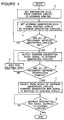
- the flow chart of Figure 4 illustrates an operation of the second embodiment.
- the steps “a” to “g” of Figure 4 correspond to the steps “A” to “G” of Figure 2, and therefore, explanation thereof will be omitted.
- the step “h” of Figure 2 illustrates the setting of the address arbitration rule to the address arbiter 110.
- each of the address generation circuits can be configured to supply a read enable signal or a write enable signal to the address arbitration circuit, and the address arbitration circuit can supply the received read enable signal or the received write enable signal to the portion or all of the address ports in accordance with the preset address arbitration rule.
- the digital processor in accordance with the present invention having a plurality of memories and a plurality of ALUs is characterized in that each of address ports of each of the memories is associated with an address generation circuit capable of executing a loop processing required for address generation.
- each of address ports of each of the memories is associated with one address generation circuit. It is possible to distribute, by use of a selector or the like, addresses generated by a limited number of address generation circuits to memories which need an address. In this case, the amount of hardware can be reduced.
Landscapes
- Engineering & Computer Science (AREA)
- Theoretical Computer Science (AREA)
- Software Systems (AREA)
- Physics & Mathematics (AREA)
- General Physics & Mathematics (AREA)
- General Engineering & Computer Science (AREA)
- Image Processing (AREA)
- Image Input (AREA)
- Memory System (AREA)
- Complex Calculations (AREA)
Claims (8)
- Processeur numérique comprenant un groupe de mémoires composé de "m" mémoires, chaque mémoire "i" (i=1 à "m") desdites "m" mémoires ayant Pi ports d'adresse "ij" (j=1 à Pi), un groupe d'unités arithmétiques et logiques composé de "n" unités arithmétiques et logiques, un premier circuit d'arbitrage recevant et arbitrant des sorties dudit groupe de mémoires pour sortir les sorties arbitrées dudit groupe de mémoires vers ledit groupe d'unités arithmétiques et logiques, et un deuxième circuit d'arbitrage recevant et arbitrant des sorties dudit groupe d'unités arithmétiques et logiques pour sortir les sorties arbitrées dudit groupe d'unités arithmétiques et logiques vers ledit groupe de mémoires,
caractérisé par une pluralité de circuits de génération d'adresse, chacun étant destiné à fournir une adresse générée audit groupe de mémoires, un circuit de fourniture d'horloge pour fournir des signaux d'horloge respectifs au moins auxdits circuits de génération d'adresse, et un circuit de commande fournissant des signaux de commande respectifs audit groupe de mémoires, audit groupe d'unités arithmétiques et logiques, audit premier circuit d'arbitrage et audit deuxième circuit d'arbitrage en synchronisme avec les signaux d'horloge générés par ledit circuit de fourniture d'horloge, ledit circuit de commande fonctionnant de manière à instaurer auparavant des règles de génération d'adresse dans lesdits circuits de génération d'adresse de telle sorte que les circuits de génération d'adresse instaurés avec les règles de génération d'adresse fonctionnent de manière à générer une adresse conformément à la règle de génération d'adresse instaurée et en synchronisme avec l'horloge fournie depuis ledit circuit de fourniture de signal d'horloge, indépendamment dudit circuit de commande, et les règles de génération d'adresse instaurées sont maintenues effectives jusqu'à ce qu'elles soient restaurées. - Processeur numérique selon la revendication 1, dans lequel chacun des circuits de génération d'adresse "ij" est connecté à chacun des ports d'adresse "ij" en une relation biunivoque.
- Processeur numérique selon la revendication 1, incluant en outre un circuit d'arbitrage d'adresse recevant les adresses générées par lesdits circuits de génération d'adresse dont chacun génère l'adresse conformément à la règle de génération d'adresse instaurée et en synchronisme avec l'horloge fournie depuis ledit circuit de fourniture de signal d'horloge, ledit circuit d'arbitrage d'adresse fournissant lesdites adresses reçues à une partie ou à la totalité desdits ports d'adresse "ij" conformément à une règle d'arbitrage d'adresse qui est instaurée par ledit circuit de commande et qui est maintenue effective jusqu'à ce qu'elle soit restaurée.
- Processeur numérique selon la revendication 1, dans lequel lesdits circuits de génération d'adresse "ij" sont configurés de manière à fournir un signal de validation de lecture ou un signal de validation d'écriture à la mémoire "i".
- Processeur numérique selon la revendication 3, dans lequel lesdits circuits de génération d'adresse "ij" sont configurés de manière à fournir un signal de validation de lecture ou un signal de validation d'écriture audit circuit d'arbitrage d'adresse, et ledit circuit d'arbitrage d'adresse fournit le signal de validation de lecture reçu ou le signal de validation d'écriture reçu à la partie ou à la totalité desdits ports d'adresse conformément à la règle d'arbitrage d'adresse préinstaurée.
- Processeur numérique selon la revendication 1, dans lequel une partie ou la totalité desdites unités arithmétiques et logiques est configurée de manière à posséder un ou plusieurs étages en pipeline.
- Processeur numérique selon la revendication 2, dans lequel une partie ou la totalité desdites unités arithmétiques et logiques est configurée de manière à posséder un ou plusieurs étages en pipeline.
- Méthode pour commander un processeur numérique selon l'une quelconque des revendications 1 à 7 qui comprend un groupe de mémoires composé de "m" mémoires, chaque mémoire "i" (i=1 à "m") desdites "m" mémoires ayant Pi ports d'adresse "ij" (j=1 à Pi), un groupe d'unités arithmétiques et logiques composé de "n" unités arithmétiques et logiques, un premier circuit d'arbitrage recevant et arbitrant des sorties dudit groupe de mémoires pour sortir les sorties arbitrées dudit groupe de mémoires vers ledit groupe d'unités arithmétiques et logiques, un deuxième circuit d'arbitrage recevant et arbitrant des sorties dudit groupe d'unités arithmétiques et logiques pour sortir les sorties arbitrées dudit groupe d'unités arithmétiques et logiques vers ledit groupe de mémoires, une pluralité de circuits de génération d'adresse, chacun étant destiné à fournir une adresse générée audit groupe de mémoires, un circuit de fourniture d'horloge pour fournir des signaux d'horloge respectifs au moins auxdits circuits de génération d'adresse, et un circuit de commande fournissant des signaux de commande respectifs audit groupe de mémoires, audit groupe d'unités arithmétiques et logiques, audit premier circuit d'arbitrage et audit deuxième circuit d'arbitrage en synchronisme avec les signaux d'horloge générés par ledit circuit de fourniture d'horloge, ledit circuit de commande fonctionnant de manière à instaurer auparavant des règles de génération d'adresse dans lesdits circuits de génération d'adresse de telle sorte que les circuits de génération d'adresse instaurés avec les règles de génération d'adresse fonctionnent de manière à générer une adresse conformément à la règle de génération d'adresse instaurée et en synchronisme avec l'horloge fournie depuis ledit circuit de fourniture de signal d'horloge, indépendamment dudit circuit de commande, et les règles de génération d'adresse instaurées sont maintenues effectives jusqu'à ce qu'elles soient restaurées, la méthode incluant les étapes de sélection d'un ou de plusieurs desdits circuits de génération d'adresse, d'instauration d'une règle de génération d'adresse dans chacun des circuits de génération d'adresse sélectionnés depuis ledit circuit de commande, de fourniture de signaux de début de génération d'adresse auxdits circuits de génération d'adresse sélectionnés depuis ledit circuit de commande simultanément ou avec une différence de temps de telle sorte que chacun desdits circuits de génération d'adresse sélectionnés commence sa génération d'adresse et continue à fournir une adresse à une mémoire correspondante en synchronisme avec ledit signal d'horloge et indépendamment dudit circuit de commande jusqu'à ce que la génération d'adresse indiquée par la règle de génération d'adresse soit achevée, chacun desdits circuits de génération d'adresse sélectionnés générant un signal de fin de génération d'adresse lorsqu'une génération d'adresse est finie, et un signal sélectionné des signaux de fin de génération d'adresse générés par lesdits circuits de génération d'adresse sélectionnés étant fourni audit circuit de commande.
Applications Claiming Priority (3)
| Application Number | Priority Date | Filing Date | Title |
|---|---|---|---|
| JP3328214A JP2906792B2 (ja) | 1991-11-15 | 1991-11-15 | ディジタルプロセッサ及びその制御方法 |
| JP32821491 | 1991-11-15 | ||
| JP328214/91 | 1991-11-15 |
Publications (3)
| Publication Number | Publication Date |
|---|---|
| EP0542318A2 EP0542318A2 (fr) | 1993-05-19 |
| EP0542318A3 EP0542318A3 (en) | 1993-09-29 |
| EP0542318B1 true EP0542318B1 (fr) | 2000-09-20 |
Family
ID=18207729
Family Applications (1)
| Application Number | Title | Priority Date | Filing Date |
|---|---|---|---|
| EP92119573A Expired - Lifetime EP0542318B1 (fr) | 1991-11-15 | 1992-11-16 | Processeur digital et méthode pour le commander |
Country Status (4)
| Country | Link |
|---|---|
| US (1) | US5475828A (fr) |
| EP (1) | EP0542318B1 (fr) |
| JP (1) | JP2906792B2 (fr) |
| DE (1) | DE69231463T2 (fr) |
Families Citing this family (4)
| Publication number | Priority date | Publication date | Assignee | Title |
|---|---|---|---|---|
| US5778416A (en) * | 1993-12-20 | 1998-07-07 | Motorola, Inc. | Parallel process address generator and method |
| DE4344157A1 (de) * | 1993-12-23 | 1995-06-29 | Philips Patentverwaltung | Funkgerät |
| JP3709553B2 (ja) * | 2000-12-19 | 2005-10-26 | インターナショナル・ビジネス・マシーンズ・コーポレーション | 演算回路および演算方法 |
| WO2019202371A1 (fr) * | 2018-04-16 | 2019-10-24 | Badenhorst Emile | Processeur et procédé d'exploitation d'un processeur |
Family Cites Families (6)
| Publication number | Priority date | Publication date | Assignee | Title |
|---|---|---|---|---|
| JPS63502535A (ja) * | 1986-02-10 | 1988-09-22 | イーストマン・コダック・カンパニー | マルチプロセッサ装置 |
| US5206940A (en) * | 1987-06-05 | 1993-04-27 | Mitsubishi Denki Kabushiki Kaisha | Address control and generating system for digital signal-processor |
| EP0551933A3 (en) * | 1987-06-05 | 1993-12-15 | Mitsubishi Electric Corp | Digital signal processor |
| US4862407A (en) * | 1987-10-05 | 1989-08-29 | Motorola, Inc. | Digital signal processing apparatus |
| KR920006283B1 (ko) * | 1988-02-19 | 1992-08-03 | 미쯔비시덴끼 가부시끼가이샤 | 디지탈신호 처리방식 |
| JP2584113B2 (ja) * | 1989-07-21 | 1997-02-19 | 松下電器産業株式会社 | データ転送方法及びデータ転送装置 |
-
1991
- 1991-11-15 JP JP3328214A patent/JP2906792B2/ja not_active Expired - Lifetime
-
1992
- 1992-11-16 DE DE69231463T patent/DE69231463T2/de not_active Expired - Fee Related
- 1992-11-16 EP EP92119573A patent/EP0542318B1/fr not_active Expired - Lifetime
- 1992-11-16 US US07/976,924 patent/US5475828A/en not_active Expired - Fee Related
Also Published As
| Publication number | Publication date |
|---|---|
| EP0542318A2 (fr) | 1993-05-19 |
| US5475828A (en) | 1995-12-12 |
| EP0542318A3 (en) | 1993-09-29 |
| DE69231463T2 (de) | 2001-04-19 |
| DE69231463D1 (de) | 2000-10-26 |
| JPH05143447A (ja) | 1993-06-11 |
| JP2906792B2 (ja) | 1999-06-21 |
Similar Documents
| Publication | Publication Date | Title |
|---|---|---|
| US5045995A (en) | Selective operation of processing elements in a single instruction multiple data stream (SIMD) computer system | |
| EP0236762B1 (fr) | Système à multiprocesseur | |
| US4553203A (en) | Easily schedulable horizontal computer | |
| EP0045634B1 (fr) | Appareil de traitement de données digitales arrangé pour l'exécution d'instructions simultanées | |
| US4980817A (en) | Vector register system for executing plural read/write commands concurrently and independently routing data to plural read/write ports | |
| US6941446B2 (en) | Single instruction multiple data array cell | |
| US5168573A (en) | Memory device for storing vector registers | |
| GB2177526A (en) | Selective operation of processing elements in a single instruction, multiple data stream (simd)computer system | |
| EP0542318B1 (fr) | Processeur digital et méthode pour le commander | |
| US4674063A (en) | Information processing apparatus having a sequence control function | |
| US4811201A (en) | Interconnect circuit | |
| US5467454A (en) | Bus use request adjusting apparatus allowing changing priority levels | |
| US4812970A (en) | Microprogram control system | |
| JPH0461390B2 (fr) | ||
| US5050076A (en) | Prefetching queue control system | |
| US6772271B2 (en) | Reduction of bank switching instructions in main memory of data processing apparatus having main memory and plural memory | |
| US6378057B1 (en) | Data processing apparatus | |
| US5600842A (en) | Microprogram controller for controlling readout of a microprogram stored in multiple storage areas | |
| JP2654451B2 (ja) | データ出力方法 | |
| US5887137A (en) | Data processing apparatus having a sorting unit to provide sorted data to a processor | |
| JP2555124B2 (ja) | 画像処理装置 | |
| JP2004062401A (ja) | 演算プロセッサおよび当該演算プロセッサを用いたカメラ装置 | |
| JP2961769B2 (ja) | 画像プロセッサ | |
| JPH02257292A (ja) | 画像メモリ用アドレス発生器 | |
| JPH04280325A (ja) | パイプライン型プロセッサ |
Legal Events
| Date | Code | Title | Description |
|---|---|---|---|
| PUAI | Public reference made under article 153(3) epc to a published international application that has entered the european phase |
Free format text: ORIGINAL CODE: 0009012 |
|
| AK | Designated contracting states |
Kind code of ref document: A2 Designated state(s): DE FR GB |
|
| PUAL | Search report despatched |
Free format text: ORIGINAL CODE: 0009013 |
|
| AK | Designated contracting states |
Kind code of ref document: A3 Designated state(s): DE FR GB |
|
| 17P | Request for examination filed |
Effective date: 19930818 |
|
| 17Q | First examination report despatched |
Effective date: 19970424 |
|
| GRAG | Despatch of communication of intention to grant |
Free format text: ORIGINAL CODE: EPIDOS AGRA |
|
| RIC1 | Information provided on ipc code assigned before grant |
Free format text: 6G 06F 9/34 A, 6G 06T 1/60 B |
|
| GRAG | Despatch of communication of intention to grant |
Free format text: ORIGINAL CODE: EPIDOS AGRA |
|
| GRAG | Despatch of communication of intention to grant |
Free format text: ORIGINAL CODE: EPIDOS AGRA |
|
| GRAH | Despatch of communication of intention to grant a patent |
Free format text: ORIGINAL CODE: EPIDOS IGRA |
|
| GRAH | Despatch of communication of intention to grant a patent |
Free format text: ORIGINAL CODE: EPIDOS IGRA |
|
| GRAA | (expected) grant |
Free format text: ORIGINAL CODE: 0009210 |
|
| AK | Designated contracting states |
Kind code of ref document: B1 Designated state(s): DE FR GB |
|
| REF | Corresponds to: |
Ref document number: 69231463 Country of ref document: DE Date of ref document: 20001026 |
|
| ET | Fr: translation filed | ||
| PLBE | No opposition filed within time limit |
Free format text: ORIGINAL CODE: 0009261 |
|
| STAA | Information on the status of an ep patent application or granted ep patent |
Free format text: STATUS: NO OPPOSITION FILED WITHIN TIME LIMIT |
|
| 26N | No opposition filed | ||
| REG | Reference to a national code |
Ref country code: GB Ref legal event code: IF02 |
|
| PGFP | Annual fee paid to national office [announced via postgrant information from national office to epo] |
Ref country code: FR Payment date: 20021108 Year of fee payment: 11 |
|
| PGFP | Annual fee paid to national office [announced via postgrant information from national office to epo] |
Ref country code: GB Payment date: 20021113 Year of fee payment: 11 |
|
| PGFP | Annual fee paid to national office [announced via postgrant information from national office to epo] |
Ref country code: DE Payment date: 20021121 Year of fee payment: 11 |
|
| PG25 | Lapsed in a contracting state [announced via postgrant information from national office to epo] |
Ref country code: GB Free format text: LAPSE BECAUSE OF NON-PAYMENT OF DUE FEES Effective date: 20031116 |
|
| PG25 | Lapsed in a contracting state [announced via postgrant information from national office to epo] |
Ref country code: DE Free format text: LAPSE BECAUSE OF NON-PAYMENT OF DUE FEES Effective date: 20040602 |
|
| GBPC | Gb: european patent ceased through non-payment of renewal fee |
Effective date: 20031116 |
|
| PG25 | Lapsed in a contracting state [announced via postgrant information from national office to epo] |
Ref country code: FR Free format text: LAPSE BECAUSE OF NON-PAYMENT OF DUE FEES Effective date: 20040730 |
|
| REG | Reference to a national code |
Ref country code: FR Ref legal event code: ST |