EP0543204A2 - Elektrischer Leistungswandler - Google Patents
Elektrischer Leistungswandler Download PDFInfo
- Publication number
- EP0543204A2 EP0543204A2 EP92118719A EP92118719A EP0543204A2 EP 0543204 A2 EP0543204 A2 EP 0543204A2 EP 92118719 A EP92118719 A EP 92118719A EP 92118719 A EP92118719 A EP 92118719A EP 0543204 A2 EP0543204 A2 EP 0543204A2
- Authority
- EP
- European Patent Office
- Prior art keywords
- positive
- modulation wave
- modulation
- negative
- wave
- Prior art date
- Legal status (The legal status is an assumption and is not a legal conclusion. Google has not performed a legal analysis and makes no representation as to the accuracy of the status listed.)
- Granted
Links
Images






Classifications
-
- H—ELECTRICITY
- H02—GENERATION; CONVERSION OR DISTRIBUTION OF ELECTRIC POWER
- H02M—APPARATUS FOR CONVERSION BETWEEN AC AND AC, BETWEEN AC AND DC, OR BETWEEN DC AND DC, AND FOR USE WITH MAINS OR SIMILAR POWER SUPPLY SYSTEMS; CONVERSION OF DC OR AC INPUT POWER INTO SURGE OUTPUT POWER; CONTROL OR REGULATION THEREOF
- H02M5/00—Conversion of AC power input into AC power output, e.g. for change of voltage, for change of frequency, for change of number of phases
-
- H—ELECTRICITY
- H02—GENERATION; CONVERSION OR DISTRIBUTION OF ELECTRIC POWER
- H02M—APPARATUS FOR CONVERSION BETWEEN AC AND AC, BETWEEN AC AND DC, OR BETWEEN DC AND DC, AND FOR USE WITH MAINS OR SIMILAR POWER SUPPLY SYSTEMS; CONVERSION OF DC OR AC INPUT POWER INTO SURGE OUTPUT POWER; CONTROL OR REGULATION THEREOF
- H02M7/00—Conversion of AC power input into DC power output; Conversion of DC power input into AC power output
- H02M7/42—Conversion of DC power input into AC power output without possibility of reversal
- H02M7/44—Conversion of DC power input into AC power output without possibility of reversal by static converters
- H02M7/48—Conversion of DC power input into AC power output without possibility of reversal by static converters using discharge tubes with control electrode or semiconductor devices with control electrode
- H02M7/483—Converters with outputs that each can have more than two voltages levels
- H02M7/487—Neutral point clamped inverters
-
- B—PERFORMING OPERATIONS; TRANSPORTING
- B60—VEHICLES IN GENERAL
- B60L—PROPULSION OF ELECTRICALLY-PROPELLED VEHICLES; SUPPLYING ELECTRIC POWER FOR AUXILIARY EQUIPMENT OF ELECTRICALLY-PROPELLED VEHICLES; ELECTRODYNAMIC BRAKE SYSTEMS FOR VEHICLES IN GENERAL; MAGNETIC SUSPENSION OR LEVITATION FOR VEHICLES; MONITORING OPERATING VARIABLES OF ELECTRICALLY-PROPELLED VEHICLES; ELECTRIC SAFETY DEVICES FOR ELECTRICALLY-PROPELLED VEHICLES
- B60L9/00—Electric propulsion with power supply external to the vehicle
- B60L9/16—Electric propulsion with power supply external to the vehicle using AC induction motors
- B60L9/18—Electric propulsion with power supply external to the vehicle using AC induction motors fed from DC supply lines
- B60L9/22—Electric propulsion with power supply external to the vehicle using AC induction motors fed from DC supply lines polyphase motors
-
- B—PERFORMING OPERATIONS; TRANSPORTING
- B60—VEHICLES IN GENERAL
- B60L—PROPULSION OF ELECTRICALLY-PROPELLED VEHICLES; SUPPLYING ELECTRIC POWER FOR AUXILIARY EQUIPMENT OF ELECTRICALLY-PROPELLED VEHICLES; ELECTRODYNAMIC BRAKE SYSTEMS FOR VEHICLES IN GENERAL; MAGNETIC SUSPENSION OR LEVITATION FOR VEHICLES; MONITORING OPERATING VARIABLES OF ELECTRICALLY-PROPELLED VEHICLES; ELECTRIC SAFETY DEVICES FOR ELECTRICALLY-PROPELLED VEHICLES
- B60L2200/00—Type of vehicles
- B60L2200/26—Rail vehicles
Definitions
- the present invention relates to an improvement of an electrical power converter arrangement which converts a DC into an AC or vice versa, and, in particular, relates to an output voltage control of such an electric power converter arrangement.
- the use of the dipolar modulation mode is desirable for an improvement of the output voltage wave forms as well as for a fine voltage regulation.
- the dipolar modulation mode necessitates pulses having opposite polarity to the output voltage to be realized, thereby the voltage utilization rate decreases. Accordingly, the transition from the dipolar modulation mode to the unipolar modulation mode is inevitable.
- the former prior art indicates that the transition between the dipolar modulation mode and the unipolar modulation mode is controlled to be carried out at a predetermined phase.
- the feet portions of the sinusoidal output voltage command can not be realized correctly. This is because that there exists a minimum on time in the switching elements constituting the electric power converter, and such a small output voltage command as in the feet portions can not be realized as the output voltage of the electric power converter.
- Fig.9 of the latter prior art illustrates a wave form which includes a fixed period ( 60° ) in dipolar modulation mode and the remaining period in unipolar modulation mode in one cycle.
- such wave form is outputted in order that a portion where the modulation wave exceeds over 1 is compensated with the other phases.
- An object of the present invention is to provide an electric power converter arrangement and an electric rolling stock control devise using the same which uninterruptedly controls the converter output voltage.
- Another object of the present invention is to provide an electric power converter arrangement and an electric rolling stock control device using the same which accurately reproduces an output voltage command in the converter output voltage.
- an electric power converter arrangement which includes a first modulation region realizing a half cycle of the output voltage by alternatively outputting positive and negative output pulses and a second modulation region realizing a half cycle of the output voltage by only outputting output pulses having the same polarity as the output voltage, and converts a DC voltage into an AC phase voltage having at least three level potentials, wherein when shifting from the first modulation region to the second modulation region, the transition is performed via a third modulation region.
- an electric power converter arrangement converting a DC voltage into an AC phase voltage having at least three level potentials which includes a third modulation region constituted by in a half cycle of the output voltage a period alternatively outputting positive and negative output pulses and another period outputting only output pulses having the same polarity as the output voltage, and further comprises means for varying these both periods.
- the unipolar modulation mode In a period wherein comparatively high output voltages such as near at the crest thereof are required the unipolar modulation mode is used, and in a period wherein comparatively low output voltages such as near at the feet thereof are required the dipolar modulation mode is used, and further, these periods are adapted to be varied, thereby, even if the output voltage command varies an output voltage which correctly corresponds to the varied voltage command is reproduced.
- an induction motor in particular, an induction motor for driving rolling stocks
- an inverter called as a three-level inverter, also called as a multi-series inverter, in which other than a high potential point of a DC power source and a low potential point thereof an intermediate potential point between these high potential point and low potential point is provided and potentials of three levels of the high potential point, the low potential point and the intermediate potential point are selectively led out at AC terminals as the phase voltage via selective on and off operation of the groups of the switching elements constituting the inverter.
- One of major features of the three-level inverter is that an AC output including small relative harmonic contents is obtained because of apparent increase of the PWM switching frequency.
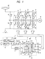
- Fig.1 The foundamental structure of the main circuit, in case of three phases, of an electric power inverter arrangement is illustrated in Fig.1.
- numeral 60 is an electric overhead line of a DC voltage source
- numerals 61 and 62 are dividing voltage capacitors for establishing an intermediate point N, hereinbelow called as a neutral point, from the DC voltage source 60
- numerals 70 ⁇ 73, 80 ⁇ 83 and 90 ⁇ 93 are self extinguishable switching elements each having a rectifying element for current circulation
- IGBTs are exemplified, however, GTOs and transistors can be used in place of the IGBTs
- numerals 74, 75, 84, 85, 94 and 95 are auxiliary rectifying elements for leading out the neutral point potential from the capacitors.
- a load in a form of an induction motor 10 is exemplified.
- switching arms 7 ⁇ 9 which are independently operable by every phase, is explained by taking up the switching arm 7 as an example.
- the conductive condition of the switching elements is determined by establishing the switching functions Sp and Sn.
- the output voltage is adjusted in substantially proportional to the inverter frequency which region is called as VVVF control region, thereby the magnetic flux within the motor is maintained substantially constant and a predetermined torque is obtained, and further, in a high speed region, the inverter frequency is successively increased while maintaining the inverter output voltage at the maximum which region is called as CVVF region, thereby the voltage utilization rate is maximized and a high speed operation is realized with the limited source voltage.
- any smaller voltage than the voltage produced by an output pulse having the minimum pulse width which is determined by the minimum on time of the switching elements can not be realized, in other words, can not be reproduced as an inverter output voltage, and thus a larger output voltage than the output voltage command is outputted.
- switching frequency Fc is expressed as follows ;
- Fc PFi (3)
- controlable minimum output voltage is limited dependent upon the characteristic illustrated by the dotted line shown in Fig.2 (b), such that there was a problem that a constinuous output voltage regulation was difficult.
- the small output voltage command is reproduced in the inverter output voltage by alternatively outputting high and low potential pulse like voltages via an intermediate potential of three levels, in that dipolar modulation.
- an inverter output voltage exactly corresponding to the output voltage command is realized by providing in a half cycle of the output voltage a period wherein high and low potential pulse like voltages are alternatively outputted via an intermediate potential among the three levels and another period wherein only output pulses having the same polarity as the output voltage are outputted, in that a combined modulation of the dipolar modulation and the unipolar modulation, which is hereinbelow called as a partial dipolar modulation.
- the output of the intermediate potential is suppressed by maximizing the output pulse width near the peak of the instantaneous output voltage and the output voltage is increased until the number of pulses contained in a half cycle of the output voltage becomes one.
- An inverter output voltage command E* is set in response to an inverter frequency Fi* as illustrated in Fig.2 (a), wherein Fcv is an inverter frequency from which the output voltage command is kept constant.
- an amplitude A of a fundamental modulation wave is set according to the following formula.
- A 2 ⁇ 2 E*/Ed (5)
- a fundamental modulation wave a1* is determined by the amplitude command A and the phase ⁇ thereof as follows ;
- a1* A sin ⁇ (6) which is illustrated in Fig.3 (a), Fig.4 (a) and Fig.5 (a).
- the amount of offset B is herein implied as a DC voltage which is superposed on the output voltage command toward a predetermined direction, in that a bias voltage.
- the positive side pulse pattern, the switching function Sp as illustrated in Fig.3 (e) and the negative side pulse pattern, the switching function Sn as illustrated in Fig.3 (f) are produced based upon the positive and negative side modulation waves ap* and an* at a pulse generation period 2Tck.
- Fig.3 (g) is an output pulse voltage appeared at the AC terminal U in the inverter arm 7 when the positive and negative side pulse patterns as shown in Fig.3 (e) and Fig.3 (f) and pulse patterns Sp ⁇ and Sn ⁇ are respectively applied to the corresponding gates of the switching elements.
- the partial dipolar modulation in a region wherein the amplitude of the output voltage command is not so high but the voltages at the feet portions of the sinusoidal wave can not be neglected. Namely, if the entire period is covered by the dipolar modulation, no problems arise with respect to reproduction of the output voltage command, however the voltage utilization rate reduces. On the other hand, if the entire output voltage command is reproduced by the unipolar modulation in order to improve the voltage utilization rate, the feet portions can not be correctly reproduced by the limitation due to the minimum on time.
- the feet portions are reproduced by making use of the dipolar modulation and the period thereof is varied depending upon the amplitude of the output voltage command.
- an output pulse voltage of a positive polarity can not be outputted by adjusting only the negative side pulse pattern, therefore a positive output voltage can not be prepared by the negative side pulse pattern.
- a negative output voltage can not be produced by the positive side pulse pattern.
- the above condition occurs in particular when shifting from the dipolar modulation mode to the unipolar modulation mode.
- the pulse pattern is determined to compensate the under voltage of a modulation wave of one polarity by another modulation wave of the opposite polarity.
- the unipolar modulation mode is explained with reference to Fig.5.
- the offset amount B When the offset amount B is reduced to 0, the two biased modulation waves ap1* and an1* as shown in Fig.5 (b) completely coincide, and as illustrated in Fig.5 (c) and (d) the positive and negative side modulation waves ap* and an* are modified as in the following formulas.
- setting of the offset amount B is important and the range of the offset amount B to be set is limited to the three regions as shown in Fig.7.
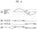
- the unipolar modulation mode is used near at the peak of the output voltage and the dipolar modulation mode is used at the feet portions of the inverter output voltage command (see Fig.4 (e), (f) and (g) ).
- the PWM mode is rendered to a two level bipolar modulation mode with no intermediate potential.
- the offset amount B is set in a range of A/2 + ⁇ 1 ⁇ B ⁇ 0.5- ⁇ 2 , wherein ⁇ 1 and ⁇ 2 : constants determined by minimum on off time, in order to maintain a predetermined zero voltage period, and the offset amount B is decreased in response to increase of the fundamental modulation wave amplitude A, thereby a smooth and constinuous pulse mode transition is achieved.
- the PWM modes shift in response to inverter frequency Fi from the dipolar modulation mode (0 ⁇ Fi ⁇ Fi) and the partial dipolar modulation mode (F1 ⁇ Fi ⁇ F2) to the unipolar modulation mode (F2 ⁇ Fi ⁇ F3), and further shifts to a three-level single pulse mode (Fi ⁇ Fcv) having indispensable intermediate potential via the overmodulation mode (F3 ⁇ Fi ⁇ Fcv) which will be explained below.
- the overmodulation region is a region wherein the offset amount B is zero and further a part of the inverter output voltage command exceeds over one.
- the transition between the dipolar modulation region, the partial dipolar modulation region and the unipolar modulation region is performed in response to such as the inverter frequency and the output voltage command corresponding thereto, thereby the torque fluctuation due to current ripple increase during the transition is suppressed and further, the harmonic components contained in the output current is reduced because even a very small output voltage command is correctly reproduced.
- the dipolar modulation is made use of at least for the VVVF region, the suppression of the torque fluctuation is achieved, however, the voltage ulilization rate during the period is reduced.
- the PWM modes are successively changed-over dependent upon increase of the inverter frequency or the vehicle speed proportional thereto.
- the dipolar modulation mode which enables to output a very small output voltage is used, after reaching to the inverter frequency F1, the PWM mode is shifted to the partial dipolar modulation region, and the PWM mode is successively shifted to the unipolar modulation region at F2, to the overmodulation region at F3 and to the single pulse modulation region at Fcv.
- the transition between the regions is performed by two methods, one is in response to the inverter frequency and the other is in response to the output voltage command.
- Fig.1 is an example of control devices for an electric inverter which outputs an AC output voltage varying between three level potentials via an on and off control of four serially connected switching element groups, in the drawing the control device for one phase is illustrated.
- a fundamental wave voltage command generator 1 is inputted of a frequency command Fi* of the inverter output voltage, an effective output voltage command E* and a DC voltage Ed, determines fundamental modulation wave A sin ⁇ and outputs the same to an amplitude command distributor 2.
- An offset setting unit 4 outputs an offset amount B, which is calculated and set dependent upon a fundamental modulation wave amplitude A to the amplitude command distributor 2.
- the amplitude command distributor 2 to which the fundamental modulation wave A sin ⁇ and the offset amount B are inputted, generates the positive and negative side modulation waves ap* and an* as illustrated in Fig.3 (c) and (d), Fig.4 (c) and (d) and Fig.5 (c) and (d).
- a pulse generation and distributor 3 to which the positive and negative side modulation waves ap* and an* are inputted, produces PWM pulse trains S1 through S4 which are determined by the switching functions Sp and Sn and are to be provided to the switching elements.
- PWM pulse trains S1 through S4 are provided to the switching elements 70 through 73 for U phase via a gate amplifier not shown to perform an on and off control of the respective switching elements.
- the phase ⁇ is obtained by time-integrating in an integrator 10 of the frequency command Fi* of the inverter output voltage which is obtained by adding operation of the slip frequency obtained based upon the deviation between a motor current command and a motor actual current and a motor rotating frequency.
- Two sinusoidal shaped biased modulation waves ap1* and an1* are prepared by adding or substracting the offset amount B set via the offset setting unit 4 dependent upon the fundamental modulation wave amplitude A to and from a signal obtained by dividing into 1/2 via a 1/2 unit 20 of the fundamental modulation wave A sin ⁇ inputted from the fundamental wave voltage command generating means 1 via adders 22 and 23.
- the fundamental modulation wave is not necessarily divided into 1/2, but if not, the constitution following thereto complexes.
- a positive side modulation wave ap* and a negative side modulation wave an* are respectively generated via polarity discrimination and destributors 24 and 25 and an adder 26, and via polarity discrimination and distributors 27 and 28 and an adder 29.
- a pulse generator 31 Based upon the positive side modulation wave ap* and the negative side modulation wave an* outputted from the amplitude command distributor 2, a pulse generator 31 produces a positive side pulse pattern corresponding to the switching function Sp and a negative side pulse pattern corresponding to the switching function Sn and generates the PWM pulse trains, in that the gate signals S1 ⁇ S4.
- the output of the fundamental wave voltage command generator 1 as shown in Fig.4 (a) is divided into 1/2 by the 1/2 unit 20 to which the above mentioned offset amount B is superposed to thereby obtain the wave forms illustrated in Fig.4 (b).
- the positive side modulation wave ap* and the negative side modulation wave an* have to be prepared, however, if the phase of the negative biased modulation wave an1* is inverted as it is to obtain the negative side modulation wave an*, the fundamental modulation wave can not correctly be reproduced in period II in the negative biased modulation wave an1*.
- the above problem is resolved by providing the polarity discrimination and distributors 24, 25, 26 and 27.
- the polarity discrimination and distributor 25 is provided so that the positive portion in the negative biased modulation wave an1* is obtained as a part of the positive side modulation wave ap*, and further, the polarity discrimination and distributor 28 is provided so that the negative portion in the positive biased modulation wave ap1* is obtained as a part of the negative side modulation wave an*.
- the positive and negative side modulation waves ap* and an* are obtained from the adders 26 and 29.
- pulse generation and distributor 3 which generates pulse patterns for turning on and off the switching elements.
- the positive and negative side pulse patterns or switching functions Sp and Sn for the output voltage are realized by the pulse generator 31.
- Clock signals CK inputted to the pulse generator 31 are reference signals which determine the pulse generation timing and the switching frequency of the switching elements.
- pulse generators 31 which is constituted by means for calculating pulse leading and trailing timings, and two timers which output pulses at the timing set in synchronism with the reference clock signals CK.
- the pulse patterns for the output voltages are classified into three according to the amplitude of the positive and negative side modulation waves ap* and an*.
- Fig.9 illustrates an example of pulse pattern generation in the dipolar modulation in period I and of pulse pattern generation in the unipolar modulation in period II.
- Fig.10 illustrates an example of pulse pattern generation wherein the absolute value of the positive or negative side modulation wave ap* or an* exceeds over 1 under the unipolar modulation (hereinbelow, called as overmodulation).
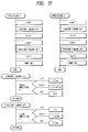
- Fig.11 shows processing flowcharts performed in the pulse generator 31 for generating the pulse patterns illustrated in Fig.9 and Fig.10.
- the leading timing Tp1 of the positive side pulse pattern Sp and the trailing timing Tn2 of the negative side pulse pattern Sn are determined based upon the following formulas depending upon the positive and negative side modulation waves ap* and an*.
- Tp1 ( 1 - ap* ) Tck (12)
- Tn2 an* Tck (13)
- Tck period of the reference signal CK.
- the timer is operating in synchronism with the reference signals CK and outputs pulses of positive and negative side pulse trains Sp and Sn at the timings illustrated in Fig.9.
- the trailing timing Tp2 of the positive side pulse pattern Sp and the leading timing Tn1 of the negative side pulse pattern Sn are obtained according to the following formulas and set in the timer (process 2).
- Tp2 ap* Tck (14)
- Tn1 (1 - an*) Tck (15)
- the dipolar modulation is realized by alternatively performing the processes 1 and 2 in synchronism with the reference signals CK.
- pulse generation continues until the amplitude of the positive or negative side modulation waves ap* or an* reduces below 1.
- the modulation mode shifts finally to the three level single pulse modulation mode.
- Tp1, Tp2, Tn1 and Tn2 are set so as to maintain a zero potential period of more than a predetermined value and a maximum output voltage of the three level inverter is outputted.
- switching frequency of the switching elements constituting the inverter main circuit is set low in the region where the inverter output frequency is low and the dipolar modulation is performed, and the switching frequency is set to increase high in accordance with the transition to the unipolar modulation, switching loss in the switching elements is kept substantially constant over the entire inverter operation regions.
- the frequency of the clock signals CK is adapted to be increased.
- the switching loss can be kept constant without modifying the other constitutions.
- a part of or all of the above pulse generating means can be, of course, realized by programed softwears.
- the offset amount B is varied based upon the fundamental modulation wave amplitude A, however when there is a predetermined relationship, such as proportioal relationship, between the fundamental modulation wave amplitude A and the inverter output frequency command, the offset value can be varied in response to the inverter output frequency command or the vehicle speed proportional thereto.
- the output voltage can be adjusted continuously and smoothly from zero voltage to the maximum voltage and further, a highly accurate and stable output voltage can be supplied.
- the positive and negative side modulation waves are away from the zero level by a predetermined value, the minimum on time is obtained without fail when PWM pulses are produced.
- a measure is contemplated wherein the pulse width is always monitored and when a pulse having a width below the minimum on time is apt to be generated the pulse is thinned out.
- the amplitude command distributor 2 is modified so as to acertain the minimum on time while taking advantage of the features of the three level inverter.
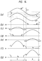
- the polarity discrimination and distributors 24, 25, 27 and 28 as shown in Fig.1 are improved as illustrated in Fig.13 so as to acertain the munimum on time.
- the polarity discrimination and distributors 240, 250, 270 and 280 are constituted in such a manner that in order to acertain the positive side minimum on time the polarity discrimination and distributor 240 is biased so as not to output an output voltage command below a predetermined value d which corresponds to the minimum on time and the corresponding portion is compensated by the negative side output voltage command.
- the biased modulation waves ap1* and an1* as illustrated in Fig. 14 (a) are respectively inputted to the polarity discrimination and distributors 240, 250, 270 and 280 of which respective output wave forms are illustrated Fig.14 (b) ⁇ (e), and the outputs, in that positive and negative side modulation waves ap* and an* from the adders 26 and 29 are those illustrated in Fig.14 (f) and (g).
- the inverter output voltage can be adjusted consinuously and smoothly from zero voltage to the maximum voltage.
Landscapes
- Engineering & Computer Science (AREA)
- Power Engineering (AREA)
- Life Sciences & Earth Sciences (AREA)
- Sustainable Development (AREA)
- Sustainable Energy (AREA)
- Transportation (AREA)
- Mechanical Engineering (AREA)
- Inverter Devices (AREA)
- Electric Propulsion And Braking For Vehicles (AREA)
- Control Of Ac Motors In General (AREA)
Applications Claiming Priority (2)
| Application Number | Priority Date | Filing Date | Title |
|---|---|---|---|
| JP301512/91 | 1991-11-18 | ||
| JP3301512A JP2765315B2 (ja) | 1991-11-18 | 1991-11-18 | 電力変換装置及びこれを利用した電気車の制御装置 |
Publications (3)
| Publication Number | Publication Date |
|---|---|
| EP0543204A2 true EP0543204A2 (de) | 1993-05-26 |
| EP0543204A3 EP0543204A3 (en) | 1993-07-21 |
| EP0543204B1 EP0543204B1 (de) | 1996-05-22 |
Family
ID=17897820
Family Applications (1)
| Application Number | Title | Priority Date | Filing Date |
|---|---|---|---|
| EP92118719A Expired - Lifetime EP0543204B1 (de) | 1991-11-18 | 1992-11-02 | Elektrischer Leistungswandler |
Country Status (6)
| Country | Link |
|---|---|
| US (1) | US5375050A (de) |
| EP (1) | EP0543204B1 (de) |
| JP (1) | JP2765315B2 (de) |
| KR (1) | KR930011391A (de) |
| CN (1) | CN1026644C (de) |
| DE (1) | DE69210955T2 (de) |
Cited By (5)
| Publication number | Priority date | Publication date | Assignee | Title |
|---|---|---|---|---|
| WO1995021486A1 (en) * | 1994-02-01 | 1995-08-10 | Unisearch Limited | Improved power converter with soft switching |
| EP1121898A1 (de) * | 2000-01-31 | 2001-08-08 | Tanita Corporation | Aus einer in einem einzigen Chip integrierten Schaltung hergestelltes Messgerät für bioelektrische Impedanz |
| EP2340957A4 (de) * | 2008-10-23 | 2014-08-06 | Mitsubishi Electric Corp | Antriebssteuervorrichtung für elektroauto |
| EP2654191A3 (de) * | 2012-04-20 | 2017-04-12 | Hamilton Sundstrand Corporation | Reduzierung von Wärmespannungen in Flugzeugmotorsteuerungen |
| EP3382882A1 (de) * | 2017-03-28 | 2018-10-03 | Schneider Electric IT Corporation | Mehrfachstatus-pwm-befehl für dreistufige wechselrichter |
Families Citing this family (23)
| Publication number | Priority date | Publication date | Assignee | Title |
|---|---|---|---|---|
| US5517401A (en) * | 1992-02-07 | 1996-05-14 | Fuji Electric Co., Ltd. | Three level pulse width modulated inverter for an electric vehicle |
| JP2814837B2 (ja) * | 1992-06-04 | 1998-10-27 | 株式会社日立製作所 | 電力変換装置 |
| US5481451A (en) * | 1992-10-30 | 1996-01-02 | Arex Electronics Corporation | AC-to-AC power inverter apparatus functioning without smoothing capacitor, and control method thereof |
| JP2888104B2 (ja) * | 1993-09-01 | 1999-05-10 | 株式会社日立製作所 | 電力変換装置 |
| US5657215A (en) * | 1995-08-29 | 1997-08-12 | Compaq Computer Corporation | Controlling switch-Mode power conversion |
| US5889668A (en) * | 1997-09-05 | 1999-03-30 | Electric Power Research Institute, Inc. | Three-phase DC-to-AC power inverter with three-level poles |
| RU2167071C1 (ru) * | 2000-09-21 | 2001-05-20 | Федеральное государственное унитарное предприятие "Центральный научно-исследовательский институт судовой электротехники и технологии" | Устройство преобразования электрической энергии |
| JP3625439B2 (ja) * | 2001-09-13 | 2005-03-02 | 東芝三菱電機産業システム株式会社 | 3レベルインバータのゲート制御装置および方法 |
| SE524014C2 (sv) * | 2002-10-09 | 2004-06-15 | Abb Ab | Omriktare samt förfarande för styrning av en omriktare |
| CN101557167B (zh) * | 2009-02-25 | 2011-02-02 | 西南交通大学 | 开关电源的双频率控制方法及其装置 |
| DE102011051548A1 (de) * | 2011-07-04 | 2013-01-10 | Sma Solar Technology Ag | Betriebsverfahren für einen Wechselrichter und netzfehlertoleranter Wechselrichter |
| JP6138413B2 (ja) | 2011-11-10 | 2017-05-31 | 三菱重工業株式会社 | モータ駆動装置 |
| CN102790399B (zh) * | 2012-07-25 | 2015-09-09 | 华为技术有限公司 | 电网无功补偿方法、装置及并网逆变器 |
| US9362840B2 (en) | 2012-10-23 | 2016-06-07 | Mitsubishi Electric Corporation | Power conversion device |
| CN105829226B (zh) * | 2013-12-18 | 2020-04-14 | 奥的斯电梯公司 | 用于再生多电平驱动器的pwm策略 |
| CN106536258B (zh) * | 2014-07-18 | 2018-09-28 | 三菱电机株式会社 | 车辆用辅助电源装置 |
| JP6426462B2 (ja) * | 2014-12-24 | 2018-11-21 | 株式会社東芝 | 電力変換装置およびその制御方法 |
| JP6937496B2 (ja) | 2018-02-16 | 2021-09-22 | ローム株式会社 | 交流電源装置 |
| US20200350833A1 (en) * | 2019-05-03 | 2020-11-05 | The Regents Of The University Of California | Pyramid-type multilevel converter topology |
| CN111030500B (zh) * | 2020-01-02 | 2021-07-20 | 阳光电源股份有限公司 | 一种逆变器的控制方法、装置及逆变器 |
| CN114447931A (zh) * | 2022-02-18 | 2022-05-06 | 中创科瑞(北京)生物科技有限公司 | 一种用于动态干扰电治疗仪的治疗控制设备 |
| CN116633179B (zh) * | 2023-05-29 | 2024-11-22 | 北京金自天正智能控制股份有限公司 | 一种三电平的低调制度载波调制方法 |
| CN118508774A (zh) * | 2024-04-10 | 2024-08-16 | 华为数字能源技术有限公司 | 一种功率变换器及逆变电路控制方法 |
Family Cites Families (5)
| Publication number | Priority date | Publication date | Assignee | Title |
|---|---|---|---|---|
| SE450317B (sv) * | 1980-12-23 | 1987-06-15 | Asea Ab | Sjelvkommuterad vexelriktare |
| ATE82093T1 (de) * | 1988-08-30 | 1992-11-15 | Siemens Ag | Verfahren zum betrieb eines dreipunktwechselrichters. |
| JP2566021B2 (ja) * | 1989-11-22 | 1996-12-25 | 三菱電機株式会社 | インバータ装置の運転方法 |
| JP2526700B2 (ja) * | 1990-04-11 | 1996-08-21 | 三菱電機株式会社 | 3相3値レベルインバ―タ |
| JP2884880B2 (ja) * | 1992-02-12 | 1999-04-19 | 株式会社日立製作所 | 電力変換器の制御装置 |
-
1991
- 1991-11-18 JP JP3301512A patent/JP2765315B2/ja not_active Expired - Fee Related
-
1992
- 1992-11-02 DE DE69210955T patent/DE69210955T2/de not_active Expired - Fee Related
- 1992-11-02 EP EP92118719A patent/EP0543204B1/de not_active Expired - Lifetime
- 1992-11-18 US US07/978,371 patent/US5375050A/en not_active Expired - Lifetime
- 1992-11-18 CN CN92113232A patent/CN1026644C/zh not_active Expired - Fee Related
- 1992-11-18 KR KR1019920021633A patent/KR930011391A/ko not_active Withdrawn
Cited By (8)
| Publication number | Priority date | Publication date | Assignee | Title |
|---|---|---|---|---|
| WO1995021486A1 (en) * | 1994-02-01 | 1995-08-10 | Unisearch Limited | Improved power converter with soft switching |
| US5742495A (en) * | 1994-02-01 | 1998-04-21 | Unisearch Limited | Power converter with soft switching |
| EP1121898A1 (de) * | 2000-01-31 | 2001-08-08 | Tanita Corporation | Aus einer in einem einzigen Chip integrierten Schaltung hergestelltes Messgerät für bioelektrische Impedanz |
| US6472888B2 (en) | 2000-01-31 | 2002-10-29 | Tanita Corporation | Bioelectrical impedance measuring apparatus constructed by one-chip integrated circuit |
| EP2340957A4 (de) * | 2008-10-23 | 2014-08-06 | Mitsubishi Electric Corp | Antriebssteuervorrichtung für elektroauto |
| EP2654191A3 (de) * | 2012-04-20 | 2017-04-12 | Hamilton Sundstrand Corporation | Reduzierung von Wärmespannungen in Flugzeugmotorsteuerungen |
| EP3382882A1 (de) * | 2017-03-28 | 2018-10-03 | Schneider Electric IT Corporation | Mehrfachstatus-pwm-befehl für dreistufige wechselrichter |
| US10461575B2 (en) | 2017-03-28 | 2019-10-29 | Schneider Electric It Corporation | Multistate PWM command for 3 levels inverters |
Also Published As
| Publication number | Publication date |
|---|---|
| DE69210955D1 (de) | 1996-06-27 |
| CN1077064A (zh) | 1993-10-06 |
| US5375050A (en) | 1994-12-20 |
| JPH05146160A (ja) | 1993-06-11 |
| KR930011391A (ko) | 1993-06-24 |
| JP2765315B2 (ja) | 1998-06-11 |
| CN1026644C (zh) | 1994-11-16 |
| DE69210955T2 (de) | 1996-11-21 |
| EP0543204B1 (de) | 1996-05-22 |
| EP0543204A3 (en) | 1993-07-21 |
Similar Documents
| Publication | Publication Date | Title |
|---|---|---|
| EP0543204B1 (de) | Elektrischer Leistungswandler | |
| EP0597132B1 (de) | Leistungswandler | |
| EP0571755B1 (de) | Leistungswandler zur Umwandlung einer Gleichspannung in eine Dreistufenwechselspannung, die eine positive, eine null- und eine negative Spannung aufweist | |
| EP0555557B1 (de) | Steuervorrichtung eines Stromrichters | |
| EP0567082B1 (de) | Steuereinrichtung für Leistungskonverter und Steuereinrichtung für Fahrzeug mit elektrischem Motor | |
| AU667014B2 (en) | Three level power converting apparatus having means for balancing DC component thereof | |
| US5298848A (en) | Large capacity variable speed PWM spatial vector type sub-harmonic system for driving AC electric motor | |
| EP0697763B1 (de) | Mehrfach gekoppelter leistungswandler und seine steuerverfahren | |
| US5680299A (en) | Electric power conversion equipment | |
| EP4092900B1 (de) | System zur steuerung einer elektrischen rotationsmaschine | |
| US5532569A (en) | Inverter control apparatus | |
| US4663578A (en) | Inverter control apparatus | |
| EP0600635B1 (de) | Mehrfachwechselrichtersystem mit parallel-geschalteten Einheiten und Steuerverfahren dafür | |
| JP3265986B2 (ja) | 電力変換器の制御装置 | |
| JP3700019B2 (ja) | 電気車の制御装置 | |
| JP3755089B2 (ja) | 電気車の制御装置 | |
| JP2005348597A (ja) | 電気車の制御装置 | |
| JPH09163755A (ja) | 電力変換装置の制御装置 | |
| JP4277360B2 (ja) | 3レベルインバータの制御装置 | |
| JP3747259B2 (ja) | 電気車の制御装置 | |
| JP3341047B2 (ja) | 多レベル電力変換装置 | |
| JP2641852B2 (ja) | 周波数変換装置 | |
| JP2005176600A (ja) | 電気車の制御装置 | |
| JPH1189243A (ja) | パルス幅変調方式インバータの制御装置 | |
| JPH09163754A (ja) | 直列多重型インバータの制御装置 |
Legal Events
| Date | Code | Title | Description |
|---|---|---|---|
| PUAI | Public reference made under article 153(3) epc to a published international application that has entered the european phase |
Free format text: ORIGINAL CODE: 0009012 |
|
| AK | Designated contracting states |
Kind code of ref document: A2 Designated state(s): CH DE FR IT LI |
|
| PUAL | Search report despatched |
Free format text: ORIGINAL CODE: 0009013 |
|
| AK | Designated contracting states |
Kind code of ref document: A3 Designated state(s): CH DE FR IT LI |
|
| 17P | Request for examination filed |
Effective date: 19930609 |
|
| 17Q | First examination report despatched |
Effective date: 19941004 |
|
| GRAH | Despatch of communication of intention to grant a patent |
Free format text: ORIGINAL CODE: EPIDOS IGRA |
|
| GRAA | (expected) grant |
Free format text: ORIGINAL CODE: 0009210 |
|
| AK | Designated contracting states |
Kind code of ref document: B1 Designated state(s): CH DE FR IT LI |
|
| REG | Reference to a national code |
Ref country code: CH Ref legal event code: NV Representative=s name: TROESCH SCHEIDEGGER WERNER AG |
|
| REF | Corresponds to: |
Ref document number: 69210955 Country of ref document: DE Date of ref document: 19960627 |
|
| ET | Fr: translation filed | ||
| ITF | It: translation for a ep patent filed | ||
| PLBE | No opposition filed within time limit |
Free format text: ORIGINAL CODE: 0009261 |
|
| STAA | Information on the status of an ep patent application or granted ep patent |
Free format text: STATUS: NO OPPOSITION FILED WITHIN TIME LIMIT |
|
| 26N | No opposition filed | ||
| PGFP | Annual fee paid to national office [announced via postgrant information from national office to epo] |
Ref country code: FR Payment date: 19980915 Year of fee payment: 7 |
|
| PGFP | Annual fee paid to national office [announced via postgrant information from national office to epo] |
Ref country code: CH Payment date: 19981020 Year of fee payment: 7 |
|
| PGFP | Annual fee paid to national office [announced via postgrant information from national office to epo] |
Ref country code: DE Payment date: 19981231 Year of fee payment: 7 |
|
| PG25 | Lapsed in a contracting state [announced via postgrant information from national office to epo] |
Ref country code: LI Free format text: LAPSE BECAUSE OF NON-PAYMENT OF DUE FEES Effective date: 19991130 Ref country code: CH Free format text: LAPSE BECAUSE OF NON-PAYMENT OF DUE FEES Effective date: 19991130 |
|
| REG | Reference to a national code |
Ref country code: CH Ref legal event code: PL |
|
| PG25 | Lapsed in a contracting state [announced via postgrant information from national office to epo] |
Ref country code: FR Free format text: LAPSE BECAUSE OF NON-PAYMENT OF DUE FEES Effective date: 20000731 |
|
| PG25 | Lapsed in a contracting state [announced via postgrant information from national office to epo] |
Ref country code: DE Free format text: LAPSE BECAUSE OF NON-PAYMENT OF DUE FEES Effective date: 20000901 |
|
| REG | Reference to a national code |
Ref country code: FR Ref legal event code: ST |
|
| PG25 | Lapsed in a contracting state [announced via postgrant information from national office to epo] |
Ref country code: IT Free format text: LAPSE BECAUSE OF NON-PAYMENT OF DUE FEES;WARNING: LAPSES OF ITALIAN PATENTS WITH EFFECTIVE DATE BEFORE 2007 MAY HAVE OCCURRED AT ANY TIME BEFORE 2007. THE CORRECT EFFECTIVE DATE MAY BE DIFFERENT FROM THE ONE RECORDED. Effective date: 20051102 |