EP0543369B1 - Modulateur de commutateur avec guides d'ondes antirésonnantes et réfléchissantes ("ARROWS") sur silicium - Google Patents
Modulateur de commutateur avec guides d'ondes antirésonnantes et réfléchissantes ("ARROWS") sur silicium Download PDFInfo
- Publication number
- EP0543369B1 EP0543369B1 EP92119714A EP92119714A EP0543369B1 EP 0543369 B1 EP0543369 B1 EP 0543369B1 EP 92119714 A EP92119714 A EP 92119714A EP 92119714 A EP92119714 A EP 92119714A EP 0543369 B1 EP0543369 B1 EP 0543369B1
- Authority
- EP
- European Patent Office
- Prior art keywords
- layer
- modulator
- interference layer
- semiconductor
- substrate
- Prior art date
- Legal status (The legal status is an assumption and is not a legal conclusion. Google has not performed a legal analysis and makes no representation as to the accuracy of the status listed.)
- Expired - Lifetime
Links
- 229910052710 silicon Inorganic materials 0.000 title claims description 17
- 239000010703 silicon Substances 0.000 title claims description 17
- 230000003287 optical effect Effects 0.000 title claims description 13
- 239000010410 layer Substances 0.000 claims description 84
- 239000004065 semiconductor Substances 0.000 claims description 25
- 239000012792 core layer Substances 0.000 claims description 24
- 239000000758 substrate Substances 0.000 claims description 22
- 238000005253 cladding Methods 0.000 claims description 21
- 238000000034 method Methods 0.000 claims description 19
- 230000000694 effects Effects 0.000 claims description 12
- VYPSYNLAJGMNEJ-UHFFFAOYSA-N Silicium dioxide Chemical compound O=[Si]=O VYPSYNLAJGMNEJ-UHFFFAOYSA-N 0.000 claims description 9
- 229910052814 silicon oxide Inorganic materials 0.000 claims description 9
- JBRZTFJDHDCESZ-UHFFFAOYSA-N AsGa Chemical compound [As]#[Ga] JBRZTFJDHDCESZ-UHFFFAOYSA-N 0.000 claims description 5
- 229910001218 Gallium arsenide Inorganic materials 0.000 claims description 5
- FTWRSWRBSVXQPI-UHFFFAOYSA-N alumanylidynearsane;gallanylidynearsane Chemical compound [As]#[Al].[As]#[Ga] FTWRSWRBSVXQPI-UHFFFAOYSA-N 0.000 claims description 4
- 230000000737 periodic effect Effects 0.000 claims description 4
- 238000005229 chemical vapour deposition Methods 0.000 claims description 3
- 238000005530 etching Methods 0.000 claims description 2
- 230000003647 oxidation Effects 0.000 claims description 2
- 238000007254 oxidation reaction Methods 0.000 claims description 2
- 238000000151 deposition Methods 0.000 claims 5
- 238000000059 patterning Methods 0.000 claims 1
- 238000007740 vapor deposition Methods 0.000 claims 1
- XUIMIQQOPSSXEZ-UHFFFAOYSA-N Silicon Chemical compound [Si] XUIMIQQOPSSXEZ-UHFFFAOYSA-N 0.000 description 13
- 239000000463 material Substances 0.000 description 9
- 230000008878 coupling Effects 0.000 description 6
- 238000010168 coupling process Methods 0.000 description 6
- 238000005859 coupling reaction Methods 0.000 description 6
- 238000004519 manufacturing process Methods 0.000 description 6
- 230000008569 process Effects 0.000 description 6
- 230000008901 benefit Effects 0.000 description 5
- 239000000969 carrier Substances 0.000 description 3
- 229920002120 photoresistant polymer Polymers 0.000 description 3
- 229910052581 Si3N4 Inorganic materials 0.000 description 2
- 239000003989 dielectric material Substances 0.000 description 2
- 239000013307 optical fiber Substances 0.000 description 2
- HQVNEWCFYHHQES-UHFFFAOYSA-N silicon nitride Chemical compound N12[Si]34N5[Si]62N3[Si]51N64 HQVNEWCFYHHQES-UHFFFAOYSA-N 0.000 description 2
- 229910008062 Si-SiO2 Inorganic materials 0.000 description 1
- 229910006403 Si—SiO2 Inorganic materials 0.000 description 1
- 238000010521 absorption reaction Methods 0.000 description 1
- 229910052782 aluminium Inorganic materials 0.000 description 1
- XAGFODPZIPBFFR-UHFFFAOYSA-N aluminium Chemical compound [Al] XAGFODPZIPBFFR-UHFFFAOYSA-N 0.000 description 1
- 230000009286 beneficial effect Effects 0.000 description 1
- 230000008859 change Effects 0.000 description 1
- 238000012938 design process Methods 0.000 description 1
- 238000000609 electron-beam lithography Methods 0.000 description 1
- 238000000407 epitaxy Methods 0.000 description 1
- 229910052732 germanium Inorganic materials 0.000 description 1
- GNPVGFCGXDBREM-UHFFFAOYSA-N germanium atom Chemical compound [Ge] GNPVGFCGXDBREM-UHFFFAOYSA-N 0.000 description 1
- 230000012447 hatching Effects 0.000 description 1
- 230000010354 integration Effects 0.000 description 1
- 238000002310 reflectometry Methods 0.000 description 1
- SBEQWOXEGHQIMW-UHFFFAOYSA-N silicon Chemical compound [Si].[Si] SBEQWOXEGHQIMW-UHFFFAOYSA-N 0.000 description 1
Images


Classifications
-
- G—PHYSICS
- G02—OPTICS
- G02F—OPTICAL DEVICES OR ARRANGEMENTS FOR THE CONTROL OF LIGHT BY MODIFICATION OF THE OPTICAL PROPERTIES OF THE MEDIA OF THE ELEMENTS INVOLVED THEREIN; NON-LINEAR OPTICS; FREQUENCY-CHANGING OF LIGHT; OPTICAL LOGIC ELEMENTS; OPTICAL ANALOGUE/DIGITAL CONVERTERS
- G02F1/00—Devices or arrangements for the control of the intensity, colour, phase, polarisation or direction of light arriving from an independent light source, e.g. switching, gating or modulating; Non-linear optics
- G02F1/01—Devices or arrangements for the control of the intensity, colour, phase, polarisation or direction of light arriving from an independent light source, e.g. switching, gating or modulating; Non-linear optics for the control of the intensity, phase, polarisation or colour
- G02F1/011—Devices or arrangements for the control of the intensity, colour, phase, polarisation or direction of light arriving from an independent light source, e.g. switching, gating or modulating; Non-linear optics for the control of the intensity, phase, polarisation or colour in optical waveguides, not otherwise provided for in this subclass
-
- G—PHYSICS
- G02—OPTICS
- G02F—OPTICAL DEVICES OR ARRANGEMENTS FOR THE CONTROL OF LIGHT BY MODIFICATION OF THE OPTICAL PROPERTIES OF THE MEDIA OF THE ELEMENTS INVOLVED THEREIN; NON-LINEAR OPTICS; FREQUENCY-CHANGING OF LIGHT; OPTICAL LOGIC ELEMENTS; OPTICAL ANALOGUE/DIGITAL CONVERTERS
- G02F1/00—Devices or arrangements for the control of the intensity, colour, phase, polarisation or direction of light arriving from an independent light source, e.g. switching, gating or modulating; Non-linear optics
- G02F1/01—Devices or arrangements for the control of the intensity, colour, phase, polarisation or direction of light arriving from an independent light source, e.g. switching, gating or modulating; Non-linear optics for the control of the intensity, phase, polarisation or colour
- G02F1/015—Devices or arrangements for the control of the intensity, colour, phase, polarisation or direction of light arriving from an independent light source, e.g. switching, gating or modulating; Non-linear optics for the control of the intensity, phase, polarisation or colour based on semiconductor elements having potential barriers, e.g. having a PN or PIN junction
- G02F1/025—Devices or arrangements for the control of the intensity, colour, phase, polarisation or direction of light arriving from an independent light source, e.g. switching, gating or modulating; Non-linear optics for the control of the intensity, phase, polarisation or colour based on semiconductor elements having potential barriers, e.g. having a PN or PIN junction in an optical waveguide structure
-
- G—PHYSICS
- G02—OPTICS
- G02F—OPTICAL DEVICES OR ARRANGEMENTS FOR THE CONTROL OF LIGHT BY MODIFICATION OF THE OPTICAL PROPERTIES OF THE MEDIA OF THE ELEMENTS INVOLVED THEREIN; NON-LINEAR OPTICS; FREQUENCY-CHANGING OF LIGHT; OPTICAL LOGIC ELEMENTS; OPTICAL ANALOGUE/DIGITAL CONVERTERS
- G02F1/00—Devices or arrangements for the control of the intensity, colour, phase, polarisation or direction of light arriving from an independent light source, e.g. switching, gating or modulating; Non-linear optics
- G02F1/01—Devices or arrangements for the control of the intensity, colour, phase, polarisation or direction of light arriving from an independent light source, e.g. switching, gating or modulating; Non-linear optics for the control of the intensity, phase, polarisation or colour
- G02F1/015—Devices or arrangements for the control of the intensity, colour, phase, polarisation or direction of light arriving from an independent light source, e.g. switching, gating or modulating; Non-linear optics for the control of the intensity, phase, polarisation or colour based on semiconductor elements having potential barriers, e.g. having a PN or PIN junction
- G02F1/0151—Devices or arrangements for the control of the intensity, colour, phase, polarisation or direction of light arriving from an independent light source, e.g. switching, gating or modulating; Non-linear optics for the control of the intensity, phase, polarisation or colour based on semiconductor elements having potential barriers, e.g. having a PN or PIN junction modulating the refractive index
- G02F1/0152—Devices or arrangements for the control of the intensity, colour, phase, polarisation or direction of light arriving from an independent light source, e.g. switching, gating or modulating; Non-linear optics for the control of the intensity, phase, polarisation or colour based on semiconductor elements having potential barriers, e.g. having a PN or PIN junction modulating the refractive index using free carrier effects, e.g. plasma effect
-
- G—PHYSICS
- G02—OPTICS
- G02F—OPTICAL DEVICES OR ARRANGEMENTS FOR THE CONTROL OF LIGHT BY MODIFICATION OF THE OPTICAL PROPERTIES OF THE MEDIA OF THE ELEMENTS INVOLVED THEREIN; NON-LINEAR OPTICS; FREQUENCY-CHANGING OF LIGHT; OPTICAL LOGIC ELEMENTS; OPTICAL ANALOGUE/DIGITAL CONVERTERS
- G02F2201/00—Constructional arrangements not provided for in groups G02F1/00 - G02F7/00
- G02F2201/06—Constructional arrangements not provided for in groups G02F1/00 - G02F7/00 integrated waveguide
- G02F2201/063—Constructional arrangements not provided for in groups G02F1/00 - G02F7/00 integrated waveguide ridge; rib; strip loaded
-
- G—PHYSICS
- G02—OPTICS
- G02F—OPTICAL DEVICES OR ARRANGEMENTS FOR THE CONTROL OF LIGHT BY MODIFICATION OF THE OPTICAL PROPERTIES OF THE MEDIA OF THE ELEMENTS INVOLVED THEREIN; NON-LINEAR OPTICS; FREQUENCY-CHANGING OF LIGHT; OPTICAL LOGIC ELEMENTS; OPTICAL ANALOGUE/DIGITAL CONVERTERS
- G02F2201/00—Constructional arrangements not provided for in groups G02F1/00 - G02F7/00
- G02F2201/30—Constructional arrangements not provided for in groups G02F1/00 - G02F7/00 grating
- G02F2201/302—Constructional arrangements not provided for in groups G02F1/00 - G02F7/00 grating grating coupler
-
- G—PHYSICS
- G02—OPTICS
- G02F—OPTICAL DEVICES OR ARRANGEMENTS FOR THE CONTROL OF LIGHT BY MODIFICATION OF THE OPTICAL PROPERTIES OF THE MEDIA OF THE ELEMENTS INVOLVED THEREIN; NON-LINEAR OPTICS; FREQUENCY-CHANGING OF LIGHT; OPTICAL LOGIC ELEMENTS; OPTICAL ANALOGUE/DIGITAL CONVERTERS
- G02F2202/00—Materials and properties
- G02F2202/10—Materials and properties semiconductor
- G02F2202/101—Ga×As and alloy
-
- G—PHYSICS
- G02—OPTICS
- G02F—OPTICAL DEVICES OR ARRANGEMENTS FOR THE CONTROL OF LIGHT BY MODIFICATION OF THE OPTICAL PROPERTIES OF THE MEDIA OF THE ELEMENTS INVOLVED THEREIN; NON-LINEAR OPTICS; FREQUENCY-CHANGING OF LIGHT; OPTICAL LOGIC ELEMENTS; OPTICAL ANALOGUE/DIGITAL CONVERTERS
- G02F2202/00—Materials and properties
- G02F2202/10—Materials and properties semiconductor
- G02F2202/105—Materials and properties semiconductor single crystal Si
Definitions
- This invention relates to an optical waveguide modulator of the type defined in the precharacterizing part of claim 1 and to the method of forming such a modulator.
- Anti-resonant Reflecting Optical Waveguides have several advantages over other types of waveguides. They can be formed upon silicon, using relatively thin layers compared to other waveguides, for easier compatibility with other electronic integrated circuits. At the same time, they can have a large mode for coupling to optical fibers. Additionally, they are relatively easy to manufacture, as they require no exotic materials.
- These waveguides typically consist of a layer of silicon oxide built upon a silicon substrate. An interference layer of silicon is then placed upon the first layer of silicon oxide, followed by another layer of silicon oxide. All of these materials can be deposited with relative ease.
- the silicon layer sandwiched between the two silicon oxide layers functions as a passive interference cladding layer. The thickness of the interference layer is not critical.
- Active optical modulators are normally difficult to produce in or on silicon Silicon exhibits no linear electro-optic effect, although changes in absorption or refractive index may be induced by modulating the density of free carriers.
- All-silicon waveguides tend to have a high propagation loss due to these same free-carrier effects and are difficult to fabricate to have a high modulation efficiency, because of poor modal overlap.
- All-dielectric waveguides can have low loss, but are typically passive and not useful for modulation. Using an ARROW structure in conjunction with vertical coupling will make it possible to combine the low-loss propagation of dielectric waveguides with the capability of modulating or switching light using free-carrier effects.
- EP-A-0 263 640 An optical waveguide of the above-mentioned type is disclosed in EP-A-0 263 640.
- this modulator is a passive modulator and has only the ability of selecting predetermined wavelengths.
- FR-A-2 647 965 discloses an optical waveguide modulator in which modulation is not done away from the main path of light in the waveguide.
- the waveguide is an Anti-Resonant Reflecting Optical Waveguide with one interference layer of a semiconductor material between two layers of dielectric material. Free-carrier effects in the interference layer are controlled by application of a current or field to an active electronic element in the layer to modulate light in the layer.
- This modulator is formed by the method of claim 12.
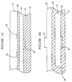
- FIG. 1A A side view of an ARROW modulator that uses the free-carrier effect in semiconductors is shown in Figure 1A.
- the modulator 10 consists of a substrate 12, which is usually, but not limited to, silicon.
- Substrate 12 has a doped or deposited area 14, which forms the gate of a transistor. The placement of the source and the drain of the transistor will be covered in further discussion.
- the lower cladding of the waveguide 16 This is normally silicon oxide.
- the interference layer 18, which, in this example, is silicon. Other semiconductor materials may also be used.
- the interference layer thickness must be such that constructive interference between the reflections from the top and bottom surfaces of this layer occurs to provide high reflectivity for the mode guided in the core layer.
- Periodic gratings 22 and 24 have been formed into the top of the interference layer 18. This can be accomplished by many ways, including etching. Although shown as two separate gratings, they could also be the two ends of a long section of grating. These gratings allow vertical coupling between the core and the interference layer.
- the core layer, 20, is deposited upon the interference layer, and is typically made out of a dielectric material with high optical transparency, such as silicon oxide, or silicon nitride.
- the lower cladding layer is chosen to be approximately one-half the thickness of the core, to prevent waveguiding in this layer.
- Figure 1B shows an end view of one embodiment of the modulator 10.
- Substrate 12 has, in addition to gate 14, source contact 26 and drain contact 28.
- the lower cladding 16 is deposited and etched, or just deposited, in such a manner as to allow the interference layer 18 to "touch down" and come in contact with the substrate 12, and its source and drain contacts. This contact allows the modulator to be controlled, if desired, by circuitry in the substrate. Alternatively, contact may be made from the top through the core layer.
- the core layer 20 has a waveguide rib, or other structure to transversely confine the light 30, the cladding underneath the edges of the core is not really necessary anyway. This allows for more freedom in the process design to manufacture the modulator.
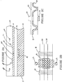
- Figure 2A shows the path of light through the modulator.
- the light enters the core layer 20 from the left of the drawing, shown as arrow 32A.
- the light travels over the grating 22 and is coupled by and through the grating into the interference layer 18, as shown by arrow 32B.
- the interference layer has a higher refractive index than the surrounding core and cladding layers, it acts as a conventional dielectric waveguide for light traveling within it.
- control circuitry, or a control element can be used to control the free-carrier concentration, and thereby modulate the light.
- One method for achieving this is to dope the interference layer to form source and drain regions, and to then apply voltage to gate 14.
- the free-carrier concentration between the source and drain regions will drop drastically in the silicon.
- the transistor may conceivably be operated in either the depletion or the enhancement mode. In either case, the changes in free-carrier concentration will result in changes in the refractive index experienced by light guided in the interference layer. For example, an increase in the free-carrier concentration will result in a decrease in the refractive index for light at the 1.3 ⁇ m wavelength.
- the control of the carrier concentration between the source and drain allows for control of the light that will eventually couple out of the interference layer.
- the previously passive layer of silicon has been turned into an active element for modulating light.
- Lateral confinement for light traveling in this layer is desirable for efficient coupling back into the laterally-confined core layer mode.
- This may be provided, for example, by doping the interference layer to change its refractive index.
- germanium could be used for raising the refractive index of a silicon layer.
- the doping forming the control element may also contribute to lateral confinement.
- FIG. 2B A possible placement of the source and drain regions is shown in Figure 2B, a top view of a modulator.
- the core layer 20 is seen from above, with rib 30 in the middle.
- Gratings 22 and 24 are shown in dashed lines. These gratings are shown etched onto the interface between the core and interference layers. The preferred placement for the gratings is on the surface of the interference layer, but they may be formed in the material either of the interference layer, or of the core layer.
- Source 27 and drain 29 are in the interference layer, and are hatched to show the active area in the silicon between them.
- Gate 14 is under this region, in or on the substrate below the lower cladding layer. It is hatched differently to highlight its location. Light will be modulated or absorbed depending on the state of the transistor, ON or OFF.
- Source 27 and drain 29 are of the same doping, either n-type or p-type, demonstrated by identical hatching.
- the gate region 14 is typically in the substrate, as in this case, and under the undoped region between the source and drain regions. The gate must be isolated electrically from the source and drain. As discussed previously, the application of voltage to this control element is used to manage the free-carrier concentration. Additionally, contact regions for the source and drain could be placed in the substrate 12, under regions 27 and 29, where these regions contact the substrate 12.
- FIG. 3A Another embodiment for control of the free-carrier effects is shown in Figures 3A and 3B.
- a top view of such an embodiment is shown in Figure 3A.
- a p-i-n diode could be used instead of the transistor in the interference layer as shown previously.
- the entire region that comprises the p-i-n diode has been shaded for viewing clarity.
- P-doped region 34 has a lower boundary at the upper edge of the confinement structure 30, as seen on the drawing.
- the i region 36 is undoped, and lies under the confinement structure 30.
- the n-doped region 38 has an upper boundary at the lower edge of confinement structure 30, as seen on the drawing.
- this structure also provides for lateral optical confinement in the intrinsic region of the interference layer.
- the p-i-n diode structure is actually easier to manufacture and allows for better control of the carrier concentration, than the configurations previously discussed.
- FIG. 3B An end view of this structure is shown in Figure 3B.
- Layer 20 is shown with the confinement structure 30.
- Region 34 the p-doped region, is to the left of the confinement structure, in the interference layer.
- the interference layer is shown making contact with the semiconductor substrate 12. This is only for electrical connection ease, and better integration of the device. There is no optical reason for this, and this should not be considered as such in the design process.
- the p-i-n diode structure controls the free-carrier concentration in the following way.
- the structure is reverse biased, the intrinsic region in the interference layer is depleted of carriers.
- carriers are injected into this region continuously, where they recombine, allowing current to flow.
- Figure 4 shows a process for manufacture for one embodiment of the invention.
- the first step, 40 is to prepare a silicon, or other semiconductor material, substrate.
- the substrate could be silicon, gallium arsenide, or other semiconductor material, and may or may not contain electronic control circuitry.
- the next step, 42 is to form the lower cladding, usually out of silicon oxide, or silicon nitride. There are many ways in which to form this layer, one of which is to use thermal oxidation, in the case of silicon.
- the cladding and core layers could be aluminum gallium arsenide (Al x Ga 1-x A s ).
- the interference layer may be gallium arsenide, or aluminum gallium arsenide with a lower aluminum concentration. This is a choice for the next step 44, in which the interference layer is formed. Again, there are many ways in which to form this layer, including epitaxy, but the preferred embodiment for the Si-SiO 2 system is normally to use chemical vapor deposition.
- the gratings or grating in the case of using only one long grating, is formed in the interference layer. This can be done many ways, one of which follows. The interference layer is coated with photoresist, and the resist is exposed to make a grating pattern. The interference layer is then etched to form the grating. Another method is to use electron beam patterning.
- Step 46 can come at various times in the process, depending on the control element used.
- the control element is the lateral p-i-n diode that is formed in the interference layer.
- the interference layer must be doped to form the p-type and n-type doped regions.
- control element step 46 would occur at a different point of the process.
- the core layer is best formed using chemical vapor deposition in step 50, selected from many possibilities.
- step 52 If the use of a confinement structure is determined to be beneficial, this can be formed in step 52.
- One possible process is as follows. First, the core layer is coated with photoresist. The photoresist is then exposed to form a pattern that defines the confinement structure, and the core layer is etched using either a wet or dry etch. Step 54 is to form the upper cladding. Depending on the environment the device is to operated in, this step may not actually be necessary. In previous discussion, the upper cladding was assumed to be air. But, if a special need arises, the upper cladding would be placed upon the core layer.
- the above invention turns a previously passive element of an ARROW waveguide into an active source of modulation. This allows for a device with all of the advantages of an ARROW waveguide discussed previously, plus the addition of modulation.
- the resultant device has thin cladding layers with a thick core layer for more efficient coupling to optical fibers.
- the dielectric core has a low loss for propagation over long distances. Additionally, the process for manufacture of such a device is compatible with standard integrated circuit processing, which leads to the additional advantage of being able to be integrated with and controlled by underlying circuitry.
Landscapes
- Physics & Mathematics (AREA)
- Nonlinear Science (AREA)
- General Physics & Mathematics (AREA)
- Optics & Photonics (AREA)
- Optical Integrated Circuits (AREA)
- Optical Couplings Of Light Guides (AREA)
Claims (19)
- Modulateur de guide d'onde optique antirésonnant et réfléchissant (10) comprenant un substrat (12), une couche de revêtement (16) située sur ledit substrat (12), une couche semiconductrice interférentielle (18) située sur ladite couche de revêtement (18), une couche (20) formant corps de guide d'onde située sur la couche semiconductrice interférentielle (18), des réseaux (22, 24) pour coupler la lumière entre ladite couche (20) formant coeur de guide d'onde et ladite couche semiconductrice interférentielle (18), ledit modulateur étant caractérisé par
un élément de commande (14) pouvant agir de manière à commander la concentration de porteurs libres dans ladite couche semiconductrice interférentielle (18), la lumière couplée par l'un desdits réseaux (22) à ladite couche interférentielle (18) étant modulée par ladite commande de ladite concentration de porteurs libres dans ladite couche interférentielle (18), puis étant couplée par un autre desdits réseaux (24) hors de ladite couche interférentielle de manière à revenir à ladite couche (20) formant coeur de guide d'onde. - Modulateur (10) selon la revendication 1, dans lequel ledit substrat (12) est en silicium.
- Modulateur (10) selon la revendication 1, dans lequel ledit substrat (12) est en arseniure de gallium.
- Modulateur (10) selon l'une quelconque des revendications précédentes, dans lequel ladite couche de revêtement (16) est en oxyde de silicium.
- Modulateur (10) selon l'une quelconque des revendications 1 à 3, dans lequel ladite couche de revêtement (16) est en arséniure d'aluminium et de gallium.
- Modulateur (10) selon l'une quelconque des revendications précédentes, dans lequel ladite couche interférentielle semiconductrice (18) est en silicium.
- Modulateur (10) selon l'une quelconque des revendications 1 à 5, dans lequel ladite couche interférentielle semiconductrice (18) est en arseniure de gallium.
- Modulateur (10) selon l'une quelconque des revendications précédentes, dans lequel ladite couche (20) formant coeur de guide d'onde est en oxyde de silicium.
- Modulateur (10) selon l'une quelconque des revendications 1 à 7, dans lequel ladite couche (20) formant corps de guide d'onde est en arseniure d'aluminium et de gallium.
- Modulateur (10) selon l'une quelconque des revendications précédentes, dans lequel ledit élément de commande (14) est un transistor.
- Modulateur (10) selon l'une quelconque des revendications 1 à 9, dans lequel ledit élément de commande (14) est une diode p-i-n.
- Procédé pour former un modulateur de guide d'onde optique antirésonnant et réfléchissant (10) comprenant les étapes consistant à préparer un substrat semiconducteur (12), former une couche de revêtement (16) sur ledit substrat (12), déposer une couche semiconductrice interférentielle (18) sur ladite couche de revêtement (16), déposer une couche (20) formant corps de guide d'onde sur ladite couche semiconductrice interférentielle (18), former dans ledit modulateur (10) des réseaux périodiques (22, 24) aptes à coupler une lumière entre ladite couche (20) formant coeur de guide d'onde et ladite couche semiconductrice interférentielle (18) ; et
former un élément de commande (14) dans ledit modulateur (10) pour commander des effets de porteurs libres dans ladite couche semiconductrice interférentielle (18) pour moduler une lumière couplée dans ladite couche semiconductrice interférentielle (18) au moyen d'un premier desdits réseaux (22), ledit élément de commande (14) étant positionné de telle sorte que ladite modulation de la lumière dans ladite couche semiconductrice interférentielle (18) est exécutée avant que ladite lumière soit transmise en retour dans ladite couche (20) formant corps de guide d'onde, par un autre desdits réseaux (24). - Procédé selon la revendication 12, selon lequel ladite étape de formation d'une couche de revêtement (16) comprend une oxydation thermique.
- Procédé selon la revendication 12 ou 13, selon lequel ladite étape de dépôt d'une couche interférentielle semiconductrice (18) comprend un dépôt en phase vapeur.
- Procédé selon l'une quelconque des revendications 12 à 14, selon lequel ladite étape de formation de réseaux périodiques (22, 24) comprend la structuration et la corrosion de ladite couche semiconductrice interférentielle (18).
- Procédé selon l'une quelconque des revendications 12 à 15, selon lequel ladite étape de dépôt d'une couche (20) formant coeur de guide d'onde comprend un dépôt chimique en phase vapeur.
- Procédé selon l'une quelconque des revendications 12 à 16, selon lequel ladite étape de formation d'un élément de commande (14) comprend un dopage de la couche semiconductrice interférentielle (18).
- Procédé selon la revendication 17, selon lequel laite étape de formation d'un élément de commande (14) comprend en outre le dopage du substrat (12).
- Procédé selon la revendication 17 ou 18, selon lequel ladite étape de formation d'un élément de commande (14) comprend en outre le dépôt d'une électrode.
Applications Claiming Priority (2)
| Application Number | Priority Date | Filing Date | Title |
|---|---|---|---|
| US797520 | 1991-11-22 | ||
| US07/797,520 US5276748A (en) | 1991-11-22 | 1991-11-22 | Vertically-coupled arrow modulators or switches on silicon |
Publications (2)
| Publication Number | Publication Date |
|---|---|
| EP0543369A1 EP0543369A1 (fr) | 1993-05-26 |
| EP0543369B1 true EP0543369B1 (fr) | 1998-01-28 |
Family
ID=25171065
Family Applications (1)
| Application Number | Title | Priority Date | Filing Date |
|---|---|---|---|
| EP92119714A Expired - Lifetime EP0543369B1 (fr) | 1991-11-22 | 1992-11-19 | Modulateur de commutateur avec guides d'ondes antirésonnantes et réfléchissantes ("ARROWS") sur silicium |
Country Status (5)
| Country | Link |
|---|---|
| US (3) | US5276748A (fr) |
| EP (1) | EP0543369B1 (fr) |
| JP (1) | JP3396498B2 (fr) |
| CA (1) | CA2080672C (fr) |
| DE (1) | DE69224272T2 (fr) |
Families Citing this family (44)
| Publication number | Priority date | Publication date | Assignee | Title |
|---|---|---|---|---|
| US5276748A (en) * | 1991-11-22 | 1994-01-04 | Texas Instruments Incorporated | Vertically-coupled arrow modulators or switches on silicon |
| US5568574A (en) * | 1995-06-12 | 1996-10-22 | University Of Southern California | Modulator-based photonic chip-to-chip interconnections for dense three-dimensional multichip module integration |
| US5577139A (en) * | 1995-08-17 | 1996-11-19 | Lucent Technologies Inc. | Integrated-circuit optical network unit |
| US5577138A (en) * | 1995-08-17 | 1996-11-19 | Lucent Technologies Inc. | Integrated-circuit optical network unit |
| CA2165119C (fr) * | 1995-12-13 | 2006-10-03 | Vincent Delisle | Guide d'ondes anti-resonant pour la selection periodique d'une serie d'au moins une longueur d'onde caracterisant un signal lunineux |
| US5903683A (en) * | 1997-09-10 | 1999-05-11 | The United States Of America As Represented By The National Security Agency | Device for modulating an optical signal using a single wave guide |
| US5987196A (en) * | 1997-11-06 | 1999-11-16 | Micron Technology, Inc. | Semiconductor structure having an optical signal path in a substrate and method for forming the same |
| US6052498A (en) * | 1997-12-19 | 2000-04-18 | Intel Corporation | Method and apparatus providing an optical input/output bus through the back side of an integrated circuit die |
| US6374003B1 (en) | 1997-12-19 | 2002-04-16 | Intel Corporation | Method and apparatus for optically modulating light through the back side of an integrated circuit die using a plurality of optical beams |
| US6075908A (en) * | 1997-12-19 | 2000-06-13 | Intel Corporation | Method and apparatus for optically modulating light through the back side of an integrated circuit die |
| US6393169B1 (en) | 1997-12-19 | 2002-05-21 | Intel Corporation | Method and apparatus for providing optical interconnection |
| US6049639A (en) * | 1997-12-19 | 2000-04-11 | Intel Corporation | Method and apparatus providing optical input/output through the back side of an integrated circuit die |
| US6330376B1 (en) | 1997-12-19 | 2001-12-11 | Intel Corporation | Higher order rejection method and apparatus for optical modulator |
| US6587605B2 (en) | 1999-01-06 | 2003-07-01 | Intel Corporation | Method and apparatus for providing optical interconnection |
| US6501092B1 (en) | 1999-10-25 | 2002-12-31 | Intel Corporation | Integrated semiconductor superlattice optical modulator |
| US6215577B1 (en) | 1999-10-25 | 2001-04-10 | Intel Corporation | Method and apparatus for optically modulating an optical beam with a multi-pass wave-guided optical modulator |
| US6268953B1 (en) | 1999-12-02 | 2001-07-31 | Intel Corporation | Method and apparatus for optically modulating an optical beam with long interaction length optical modulator |
| US6351326B1 (en) | 1999-12-14 | 2002-02-26 | Intel Corporation | Method and apparatus for optically modulating light utilizing a resonant cavity structure |
| GB2373343A (en) * | 2001-03-16 | 2002-09-18 | Bookham Technology Plc | Rib waveguide for connection to an optical component |
| US6654511B2 (en) | 2001-05-17 | 2003-11-25 | Sioptical, Inc. | Optical modulator apparatus and associated method |
| US6526187B1 (en) | 2001-05-17 | 2003-02-25 | Optronx, Inc. | Polarization control apparatus and associated method |
| US6912330B2 (en) | 2001-05-17 | 2005-06-28 | Sioptical Inc. | Integrated optical/electronic circuits and associated methods of simultaneous generation thereof |
| US6493502B1 (en) | 2001-05-17 | 2002-12-10 | Optronx, Inc. | Dynamic gain equalizer method and associated apparatus |
| US6690844B2 (en) | 2001-05-17 | 2004-02-10 | Optronx, Inc. | Optical fiber apparatus and associated method |
| US6891685B2 (en) * | 2001-05-17 | 2005-05-10 | Sioptical, Inc. | Anisotropic etching of optical components |
| US6748125B2 (en) | 2001-05-17 | 2004-06-08 | Sioptical, Inc. | Electronic semiconductor control of light in optical waveguide |
| US6625348B2 (en) | 2001-05-17 | 2003-09-23 | Optron X, Inc. | Programmable delay generator apparatus and associated method |
| US6603889B2 (en) | 2001-05-17 | 2003-08-05 | Optronx, Inc. | Optical deflector apparatus and associated method |
| US6947615B2 (en) | 2001-05-17 | 2005-09-20 | Sioptical, Inc. | Optical lens apparatus and associated method |
| AU2002305612A1 (en) * | 2001-05-17 | 2002-11-25 | Optronx, Inc. | Electronic semiconductor control of light in optical waveguide |
| US6608945B2 (en) | 2001-05-17 | 2003-08-19 | Optronx, Inc. | Self-aligning modulator method and associated apparatus |
| US6646747B2 (en) | 2001-05-17 | 2003-11-11 | Sioptical, Inc. | Interferometer apparatus and associated method |
| US6963118B2 (en) * | 2001-05-17 | 2005-11-08 | Sioptical, Inc. | Hybrid active and electronic circuit with evanescent coupling |
| US6999662B2 (en) * | 2001-11-15 | 2006-02-14 | UNIVERSITé LAVAL | Segmented waveguide array grating filters |
| US6993224B1 (en) | 2001-11-15 | 2006-01-31 | UNIVERSITé LAVAL | Segmented waveguide array gratings (SWAG)-based archival optical memory |
| US6580864B1 (en) * | 2002-01-14 | 2003-06-17 | Applied Wdm, Inc. | Birefringence free optical waveguide structures |
| KR100418262B1 (ko) * | 2002-05-14 | 2004-02-14 | 한국전자통신연구원 | 다중 모드 간섭형 결합기, 이를 이용한 다층 평면형광도파로 및 그 제조 방법 |
| US6993236B1 (en) * | 2002-06-24 | 2006-01-31 | Luxtera, Inc. | Polysilicon and silicon dioxide light scatterers for silicon waveguides on five layer substrates |
| US7010208B1 (en) * | 2002-06-24 | 2006-03-07 | Luxtera, Inc. | CMOS process silicon waveguides |
| WO2005082091A2 (fr) * | 2004-02-26 | 2005-09-09 | Sioptical, Inc. | Manipulation active de la lumiere dans une structure de silicium sur isolant (soi) |
| US8031991B2 (en) * | 2008-05-28 | 2011-10-04 | Lightwire Inc. | Low index, large mode field diameter optical coupler |
| SE1051151A1 (sv) * | 2010-11-03 | 2012-05-04 | Brokk Ab | Brythammare vid en med manöverbar arm utrustad arbetsmaskin |
| JP2015064413A (ja) * | 2013-09-24 | 2015-04-09 | 富士通株式会社 | 光半導体素子とその製造方法 |
| US9726913B2 (en) * | 2014-01-30 | 2017-08-08 | Awenyx Inc. | Semiconductor interferometric device |
Family Cites Families (13)
| Publication number | Priority date | Publication date | Assignee | Title |
|---|---|---|---|---|
| GB2169134B (en) * | 1984-11-16 | 1988-11-16 | Canon Kk | Multibeam emitting device |
| US4715672A (en) * | 1986-01-06 | 1987-12-29 | American Telephone And Telegraph Company | Optical waveguide utilizing an antiresonant layered structure |
| US4745607A (en) * | 1986-10-08 | 1988-05-17 | American Telephone And Telegraph Company, At&T Bell Laboratories | Interlayer directional coupling in antiresonant reflecting optical waveguides |
| EP0309744A3 (fr) * | 1987-09-29 | 1989-06-28 | Siemens Aktiengesellschaft | Structure avec guide d'onde qui s'étend de manière plane |
| US4904045A (en) * | 1988-03-25 | 1990-02-27 | American Telephone And Telegraph Company | Grating coupler with monolithically integrated quantum well index modulator |
| FR2647965A1 (fr) * | 1989-05-30 | 1990-12-07 | Thomson Csf | Modulateur electro-optique du type transistor a effet de champ |
| DE3931588A1 (de) * | 1989-09-22 | 1991-04-04 | Standard Elektrik Lorenz Ag | Interferometrischer halbleiterlaser |
| JPH03228032A (ja) * | 1990-02-01 | 1991-10-09 | Mitsubishi Electric Corp | 光方向性結合器 |
| DE4011860A1 (de) * | 1990-04-09 | 1991-10-10 | Siemens Ag | Halbleiterelement mit einer silizium-schicht |
| EP0466082B1 (fr) * | 1990-07-09 | 1997-05-02 | Canon Kabushiki Kaisha | Procédé pour la modulation de la lumière et modulateur optique |
| US5165105A (en) * | 1991-08-02 | 1992-11-17 | Minnesota Minning And Manufacturing Company | Separate confinement electroabsorption modulator utilizing the Franz-Keldysh effect |
| US5276748A (en) * | 1991-11-22 | 1994-01-04 | Texas Instruments Incorporated | Vertically-coupled arrow modulators or switches on silicon |
| US5253314A (en) * | 1992-01-31 | 1993-10-12 | At&T Bell Laboratories | Tunable optical waveguide coupler |
-
1991
- 1991-11-22 US US07/797,520 patent/US5276748A/en not_active Expired - Lifetime
-
1992
- 1992-10-15 CA CA002080672A patent/CA2080672C/fr not_active Expired - Fee Related
- 1992-11-19 DE DE69224272T patent/DE69224272T2/de not_active Expired - Fee Related
- 1992-11-19 EP EP92119714A patent/EP0543369B1/fr not_active Expired - Lifetime
- 1992-11-20 JP JP31232192A patent/JP3396498B2/ja not_active Expired - Fee Related
-
1993
- 1993-07-30 US US08/100,837 patent/US5367582A/en not_active Expired - Lifetime
-
1994
- 1994-11-07 US US08/335,233 patent/US5502779A/en not_active Expired - Lifetime
Also Published As
| Publication number | Publication date |
|---|---|
| CA2080672A1 (fr) | 1993-05-23 |
| DE69224272T2 (de) | 1998-07-23 |
| US5367582A (en) | 1994-11-22 |
| US5276748A (en) | 1994-01-04 |
| DE69224272D1 (de) | 1998-03-05 |
| JP3396498B2 (ja) | 2003-04-14 |
| JPH06202052A (ja) | 1994-07-22 |
| CA2080672C (fr) | 2002-09-24 |
| EP0543369A1 (fr) | 1993-05-26 |
| US5502779A (en) | 1996-03-26 |
Similar Documents
| Publication | Publication Date | Title |
|---|---|---|
| EP0543369B1 (fr) | Modulateur de commutateur avec guides d'ondes antirésonnantes et réfléchissantes ("ARROWS") sur silicium | |
| US4840446A (en) | Photo semiconductor device having a multi-quantum well structure | |
| JP2681044B2 (ja) | 光変調器 | |
| US6633692B2 (en) | High carrier injection optical waveguide switch | |
| US5825047A (en) | Optical semiconductor device | |
| EP1729382B1 (fr) | Dispositif de collimation de type guide d'ondes parabolique et diode laser accordable à cavité externe comprenant celle-ci | |
| US5048907A (en) | Electric field induced quantum well waveguides | |
| JP2873062B2 (ja) | 光集積装置およびその製造方法 | |
| EP0385685B1 (fr) | Dispositif à semi-conducteur contenant des hétérostructures à puits quantiques à modulation de dopage en cascade | |
| US4943133A (en) | Low loss semiconductor optical phase modulator | |
| US4796274A (en) | Semiconductor device with distributed bragg reflector | |
| US5862168A (en) | Monolithic integrated optical semiconductor component | |
| US4746183A (en) | Electrically controlled integrated optical switch | |
| US6995454B2 (en) | Semiconductor optical integrated device having a light emitting portion, a modulation section and a separation portion | |
| US7865053B2 (en) | Multi-semiconductor slab electro-optic modulator and process for using the same | |
| JP2002503825A (ja) | 光学構造体および光学構造体を製造するための方法 | |
| US4744616A (en) | Monolithic electro-optic modulator array | |
| US5581108A (en) | Optical Switching device | |
| Oh et al. | A very low operation current InGaAsP/InP total internal reflection optical switch using p/n/p/n current blocking layers | |
| GB2265252A (en) | An electro-optic device | |
| JP7816512B2 (ja) | 光変調器 | |
| JPH06130236A (ja) | 交差型光スイッチ | |
| Mikami et al. | InGaAsP/InP optical waveguide switch operated by a carrier-induced change in the refractive index | |
| JP7276452B2 (ja) | 光変調器 | |
| JPS60173519A (ja) | 半導体光スイツチ |
Legal Events
| Date | Code | Title | Description |
|---|---|---|---|
| PUAI | Public reference made under article 153(3) epc to a published international application that has entered the european phase |
Free format text: ORIGINAL CODE: 0009012 |
|
| AK | Designated contracting states |
Kind code of ref document: A1 Designated state(s): DE FR GB IT NL |
|
| 17P | Request for examination filed |
Effective date: 19930921 |
|
| 17Q | First examination report despatched |
Effective date: 19950523 |
|
| GRAG | Despatch of communication of intention to grant |
Free format text: ORIGINAL CODE: EPIDOS AGRA |
|
| GRAG | Despatch of communication of intention to grant |
Free format text: ORIGINAL CODE: EPIDOS AGRA |
|
| GRAH | Despatch of communication of intention to grant a patent |
Free format text: ORIGINAL CODE: EPIDOS IGRA |
|
| GRAH | Despatch of communication of intention to grant a patent |
Free format text: ORIGINAL CODE: EPIDOS IGRA |
|
| GRAA | (expected) grant |
Free format text: ORIGINAL CODE: 0009210 |
|
| ITF | It: translation for a ep patent filed | ||
| AK | Designated contracting states |
Kind code of ref document: B1 Designated state(s): DE FR GB IT NL |
|
| REF | Corresponds to: |
Ref document number: 69224272 Country of ref document: DE Date of ref document: 19980305 |
|
| ET | Fr: translation filed | ||
| PLBE | No opposition filed within time limit |
Free format text: ORIGINAL CODE: 0009261 |
|
| STAA | Information on the status of an ep patent application or granted ep patent |
Free format text: STATUS: NO OPPOSITION FILED WITHIN TIME LIMIT |
|
| 26N | No opposition filed | ||
| REG | Reference to a national code |
Ref country code: GB Ref legal event code: IF02 |
|
| PGFP | Annual fee paid to national office [announced via postgrant information from national office to epo] |
Ref country code: IT Payment date: 20061130 Year of fee payment: 15 |
|
| PGFP | Annual fee paid to national office [announced via postgrant information from national office to epo] |
Ref country code: DE Payment date: 20071130 Year of fee payment: 16 Ref country code: NL Payment date: 20071010 Year of fee payment: 16 |
|
| PGFP | Annual fee paid to national office [announced via postgrant information from national office to epo] |
Ref country code: FR Payment date: 20071105 Year of fee payment: 16 Ref country code: GB Payment date: 20071005 Year of fee payment: 16 |
|
| GBPC | Gb: european patent ceased through non-payment of renewal fee |
Effective date: 20081119 |
|
| PG25 | Lapsed in a contracting state [announced via postgrant information from national office to epo] |
Ref country code: NL Free format text: LAPSE BECAUSE OF NON-PAYMENT OF DUE FEES Effective date: 20090601 |
|
| NLV4 | Nl: lapsed or anulled due to non-payment of the annual fee |
Effective date: 20090601 |
|
| PG25 | Lapsed in a contracting state [announced via postgrant information from national office to epo] |
Ref country code: IT Free format text: LAPSE BECAUSE OF NON-PAYMENT OF DUE FEES Effective date: 20071119 |
|
| REG | Reference to a national code |
Ref country code: FR Ref legal event code: ST Effective date: 20090731 |
|
| PG25 | Lapsed in a contracting state [announced via postgrant information from national office to epo] |
Ref country code: DE Free format text: LAPSE BECAUSE OF NON-PAYMENT OF DUE FEES Effective date: 20090603 |
|
| PG25 | Lapsed in a contracting state [announced via postgrant information from national office to epo] |
Ref country code: GB Free format text: LAPSE BECAUSE OF NON-PAYMENT OF DUE FEES Effective date: 20081119 |
|
| PG25 | Lapsed in a contracting state [announced via postgrant information from national office to epo] |
Ref country code: FR Free format text: LAPSE BECAUSE OF NON-PAYMENT OF DUE FEES Effective date: 20081130 |