EP0543565A1 - Verbindungsstruktur für elektrische Signale mit hoher Geschwindigkeit - Google Patents
Verbindungsstruktur für elektrische Signale mit hoher Geschwindigkeit Download PDFInfo
- Publication number
- EP0543565A1 EP0543565A1 EP92310328A EP92310328A EP0543565A1 EP 0543565 A1 EP0543565 A1 EP 0543565A1 EP 92310328 A EP92310328 A EP 92310328A EP 92310328 A EP92310328 A EP 92310328A EP 0543565 A1 EP0543565 A1 EP 0543565A1
- Authority
- EP
- European Patent Office
- Prior art keywords
- unit
- ram
- units
- center
- cluster
- Prior art date
- Legal status (The legal status is an assumption and is not a legal conclusion. Google has not performed a legal analysis and makes no representation as to the accuracy of the status listed.)
- Granted
Links
Images

Classifications
-
- H—ELECTRICITY
- H10—SEMICONDUCTOR DEVICES; ELECTRIC SOLID-STATE DEVICES NOT OTHERWISE PROVIDED FOR
- H10D—INORGANIC ELECTRIC SEMICONDUCTOR DEVICES
- H10D86/00—Integrated devices formed in or on insulating or conducting substrates, e.g. formed in silicon-on-insulator [SOI] substrates or on stainless steel or glass substrates
- H10D86/40—Integrated devices formed in or on insulating or conducting substrates, e.g. formed in silicon-on-insulator [SOI] substrates or on stainless steel or glass substrates characterised by multiple TFTs
- H10D86/441—Interconnections, e.g. scanning lines
-
- G—PHYSICS
- G11—INFORMATION STORAGE
- G11C—STATIC STORES
- G11C7/00—Arrangements for writing information into, or reading information out from, a digital store
- G11C7/10—Input/output [I/O] data interface arrangements, e.g. I/O data control circuits, I/O data buffers
-
- G—PHYSICS
- G11—INFORMATION STORAGE
- G11C—STATIC STORES
- G11C5/00—Details of stores covered by group G11C11/00
-
- G—PHYSICS
- G11—INFORMATION STORAGE
- G11C—STATIC STORES
- G11C5/00—Details of stores covered by group G11C11/00
- G11C5/06—Arrangements for interconnecting storage elements electrically, e.g. by wiring
- G11C5/063—Voltage and signal distribution in integrated semi-conductor memory access lines, e.g. word-line, bit-line, cross-over resistance, propagation delay
-
- G—PHYSICS
- G11—INFORMATION STORAGE
- G11C—STATIC STORES
- G11C7/00—Arrangements for writing information into, or reading information out from, a digital store
- G11C7/22—Read-write [R-W] timing or clocking circuits; Read-write [R-W] control signal generators or management
-
- H—ELECTRICITY
- H05—ELECTRIC TECHNIQUES NOT OTHERWISE PROVIDED FOR
- H05K—PRINTED CIRCUITS; CASINGS OR CONSTRUCTIONAL DETAILS OF ELECTRIC APPARATUS; MANUFACTURE OF ASSEMBLAGES OF ELECTRICAL COMPONENTS
- H05K1/00—Printed circuits
- H05K1/18—Printed circuits structurally associated with non-printed electric components
-
- H—ELECTRICITY
- H05—ELECTRIC TECHNIQUES NOT OTHERWISE PROVIDED FOR
- H05K—PRINTED CIRCUITS; CASINGS OR CONSTRUCTIONAL DETAILS OF ELECTRIC APPARATUS; MANUFACTURE OF ASSEMBLAGES OF ELECTRICAL COMPONENTS
- H05K2201/00—Indexing scheme relating to printed circuits covered by H05K1/00
- H05K2201/10—Details of components or other objects attached to or integrated in a printed circuit board
- H05K2201/10007—Types of components
- H05K2201/10159—Memory
-
- H—ELECTRICITY
- H05—ELECTRIC TECHNIQUES NOT OTHERWISE PROVIDED FOR
- H05K—PRINTED CIRCUITS; CASINGS OR CONSTRUCTIONAL DETAILS OF ELECTRIC APPARATUS; MANUFACTURE OF ASSEMBLAGES OF ELECTRICAL COMPONENTS
- H05K2201/00—Indexing scheme relating to printed circuits covered by H05K1/00
- H05K2201/10—Details of components or other objects attached to or integrated in a printed circuit board
- H05K2201/10431—Details of mounted components
- H05K2201/10507—Involving several components
- H05K2201/10545—Related components mounted on both sides of the PCB
-
- H—ELECTRICITY
- H05—ELECTRIC TECHNIQUES NOT OTHERWISE PROVIDED FOR
- H05K—PRINTED CIRCUITS; CASINGS OR CONSTRUCTIONAL DETAILS OF ELECTRIC APPARATUS; MANUFACTURE OF ASSEMBLAGES OF ELECTRICAL COMPONENTS
- H05K2201/00—Indexing scheme relating to printed circuits covered by H05K1/00
- H05K2201/10—Details of components or other objects attached to or integrated in a printed circuit board
- H05K2201/10613—Details of electrical connections of non-printed components, e.g. special leads
- H05K2201/10621—Components characterised by their electrical contacts
- H05K2201/10689—Leaded Integrated Circuit [IC] package, e.g. dual-in-line [DIL]
Definitions
- the present invention relates to a high speed electrical signal interconnect structure for transferring data, and in particular, the present invention relates to an optimum interconnect structure among multiple Dynamic Random Access Memory devices in order to accommodate high speed signals.
- SIMM Single In-line Memory Modules
- RAM random access memory
- DRAM Dynamic RAM
- SRAM Static RAM
- VRAM Video RAM
- DRAMs store information in integrated circuits that contain capacitors. Because capacitors lose their charge over time, DRAMs must include logic to "refresh” (recharge) the RAM chips periodically. While a DRAM is being refreshed, it cannot be read by the processor; if the processor must read the RAM while it is being refreshed, one or more wait states occur. Because their internal circuitry is simple, DRAMs are more commonly used than SRAMs , even though they are slower. A DRAM can hold approximately four times as much data per area as a SRAM of the same complexity.
- SRAM is based on the logic circuit known as the flip-flop, which retains the information stored as long as there is enough power to run the device. Because SRAMs are more expensive than DRAMs, SRAMs are usually reserved for special fast memory subsystems called caches, in which frequently used data values are stored for quick access.
- VRAM is a special type of DRAM used in high-speed video applications. With conventional DRAM, both the processor and the video circuitry must access RAM by sharing the same control pins on the RAM chips. VRAM provides separate pins for the processor and the video circuitry. The processor accesses the VRAM in a manner almost identical to that for DRAM, but the video circuitry is provided with a special "back door" to the VRAM. This back door lets the video circuitry access the memory bit by bit (serially), which is more appropriate for transferring pixels to the screen than is the parallel access provided by conventional DRAM.
- a driver is a hardware device that controls or regulates another device.
- a line driver for example, boosts signals transmitted over a communications line, and a bus driver amplifies and regulates signals transmitted over a bus (data pathway) thereby providing a strong signal across multiple lines concurrently. Doubling or quadrupling the number of RAM chips on a SIMM will result in a corresponding increase in the SIMM load seen by the bus driver. Such an increase in load would exceed the capability of the bus driver.
- SIMM boards While it is common in the art for SIMM boards to have a plurality of DRAM modules on a SIMM, the driver is typically located on a separate board with a significantly long interconnect between the driver on the board and the memory modules located on the SIMM. Most SIMMs only contain memory chips, thereby relying on the bus driver to supply the signals to the memory chips. Some prior art SIMM boards have an on-board driver for each memory module. However, simply adding on-board drivers will not maintain the signal integrity requirements necessary in the case of a high density, high speed memory module.
- a single on-board driver also may not have the power to drive such a large number of chips.
- increasing the number, and hence, the density of the RAM chips on the SIMM board necessarily increases the length of the signal paths used to connect the chips together.
- each RAM chip must be connected to a single signal source. The physical size of each individual RAM chip forces the chips to be disbursed across the SIMM board in such a way that longer lead lengths cannot be avoided. Increased lead lengths cause reflection signal noise which can cause glitches (non-monotonic wave forms). Non-monotonic waveforms appear as multiple rising edges, where only one rising edge was desired. These glitches can result in the wrong data being stored in, or retrieved from, the memory thereby destroying the reliability of the computer's computations.
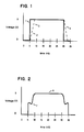
- the square wave 1 represents an ideal signal.
- Voltage on the line may be in either of two states (low or high). These states may be thought of as corresponding to two arbitrary opposite states which have been chosen for their suitability based upon the particular function of the signal. Representative naming conventions include: on/off, zero(0)/one(1), Read/Write.
- the speed of the signal is judged by the number of possible times per second that the signal can transition from one state to another. Thus for a typical high speed signal with a frequency of 40 Megahertz, the signal would have a maximum of 40 million high/low states per second. Each state would last 25 nanoseconds (billionths of a second).
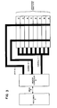
- the time that it takes for the signal to reflect back is a function of the speed of light, the length of travel of the signal along its path and the dielectric constant of the board. For a fixed dielectric constant, the relationship is such that the longer the length of the signal path, the longer the delay to the inflection point.
- the signal has several terminal points, then there will be as many inflection points as there are different length paths to the terminal points and combination of inflection points may produce false triggers.
- the connection distances are short enough so that false triggers do not occur. This is because the wave returns during the risetime period of the signal.
- a high speed, high density Dynamic Random Access Memory (DRAM) Single In-line Memory Module (SIMM) which contains an on-board buffer for driving time critical signals from a single source and further includes innovative signal trace routing having closely equivalent minimum signal line lengths and vias to memory modules on the front and back surfaces of the circuit board resulting in a high speed, high density SIMM with clean rising/falling signal edges.
- DRAM Dynamic Random Access Memory
- SIMM Single In-line Memory Module
- Time critical signals from the memory controller of a computer RAM system are sent to a SIMM.
- a driving chip located in the center of the printed circuit board of the SIMM, acts as a buffer and drives various signals to the DRAM chips populating the board. Specifically, the driver drives the Column Address Strobe (CAS), Row Address Strobe (RAS) and Write Enable (WE) signals.
- CAS Column Address Strobe
- RAS Row Address Strobe
- WE Write Enable
- the present invention further includes symmetric, minimum distance, signal line traces that electrically connect the driving chip to clusters of DRAM chips.
- the DRAM chip clusters populate both sides of the printed circuit board with DRAM chips on one side of the board having connector pins located on the chips such that the chips are mirror images of the DRAM chips on the opposite side of the board.
- Time critical signals are delivered to input pins of DRAM chips on the side of the printed circuit board opposite the driving chip by vias that extend through the multiple layers of the printed circuit board from the corresponding signal input pins of each chip's corresponding mirror image chip.
- the lengths of the signal line traces are decreased sufficiently such that signal reflections harmlessly occur during the signal transitions.
- the DRAMS on the opposite side of the board are mirror images of those on the front side. Thus, only one set of traces is needed to connect the front side DRAMs as the back side is connected with vias. This cuts the trace capacitance in half, since the back side DRAMS do not have a separate set of traces routed from the driving chip.
- the present invention provides a high speed, high density SIMM apparatus with clean rising/falling signal edges heretofore unknown in the prior art.
- Figure 1 illustrates the risetime delay in an actual versus theoretical signal.
- Figure 2 illustrates a signal that includes a line delay reflection glitch.
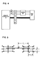
- FIG. 3 illustrates the RAM system environment that utilizes the present invention.
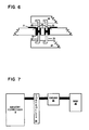
- Figure 4 illustrates a Single In-line Memory Module utilizing the teachings of the present invention.
- Figure 5 illustrates a minimum trace length star cluster configuration of the present invention.
- Figure 6 illustrates the mounting of a RAM chip and its mirror image directly opposite each other on opposite sides of a circuit board and electrical connection of the RAM chips through the board.
- Figure 7 illustrates an alternate embodiment of a Single In-line Memory Module utilizing the teachings of the present invention.
- Figure 8 illustrates another minimum trace length star cluster configuration of the alternate embodiment of the present invention with the lower trace capacitance than Figure 5 ..
- a high speed, high density Dynamic Random Access Memory (DRAM) Single In-line Memory Module (SIMM) which contains an on-board buffer for driving time critical signals from a single source and further includes innovative signal trace routing having closely equivalent minimum signal line lengths and vias to memory modules on the front and back surfaces of the circuit board resulting in a high speed, high density memory SIMM with clean rising/falling signal edges is disclosed.
- DRAM Dynamic Random Access Memory
- SIMM Single In-line Memory Module
- the present invention has been designed to operate in a RAM system such as is described by this diagram.
- address and data signals are carried between the memory controller 8 and processor 9 by the 64 bit bus 10.
- the memory controller 8 then controls the flow of Control 11 (3 bit), Data 12 (144 bit) and Address 13 (11 bit) signals to each of eight DRAM/VRAM SIMM slots 14-21.
- Each of the eight SIMM slots is a hardware connector into which VRAM or DRAM SIMMs can be inserted.
- the present invention can be used by inserting it into any of the eight SIMM slots.
- the present invention uses a single driving chip on the SIMM board to provide various time critical signals to the DRAM modules on the SIMM.
- the driving clip best mode implementation of the present invention is the Texas Instruments, Inc. model number 74ABT16244, however it can be appreciated by one skilled in the art that another driver may also be used.
- Column Address Strobe (CAS) 22, Row Address Strobe (RAS) 23 and Write Enable (WE) 24 signals come through the SIMM connector 25 from the Memory Controller 8 to the on-board driving chip 26.
- the time critical signals are then routed from the driver 26 to each of the DRAM chips 26.
- the time critical signals, including data and address, are carried directly from the SIMM connector 25 to the DRAM chips 27. However, it will be appreciated by one skilled in the art that these less time critical signals could also be driven by an on-board driver.
- the driving chip 26 is located in the center of eighteen DRAM chips 28-45 which are positioned in a symmetric pattern.
- the driving chip is connected electrically to the two center DRAM chips 28 & 29.
- the two center DRAM chips 28 & 29 are connected electrically in the vertical direction to the two closest DRAM chips 30-33 & 34-37.
- each DRAM chip 28-45 is connected electrically in the horizontal direction to its closest neighbor DRAM chip 28-45.
- the distances X1, Y1 and Z1 correspond approximately to one inch, one-half inch and two inches, respectively.
- a RAM chip 65 is mounted to a double sided circuit board 66 with a mirror image RAM chip 67 mounted on the other side.
- the RAM chip 65 is identical to the mirror image RAM chip 67 except that the leads of the RAM chip are mirror images of the leads of the mirror image RAM chip. That is to say, in this example, looking from the top of the chips, the front left pin 68 of the RAM chip 65 serves the same electrical function as the front right pin 69 of the mirror image RAM chip 67.
- the RAM chip 65 and its mirror image RAM chip 67 are mounted opposite each other on the circuit board 66 in such a manner that the front left pin 68 of the RAM chip 65 is connected electrically to the front right pin 69 of the mirror image RAM chip 67 through the circuit board 66 by a via 70 which is also connected electrically to a signal trace 71 which serves both pins.
- the second pin from the front 72 on the left side of the RAM chip 65 corresponds to the second pin from the front 73 on the right side of the mirror image RAM chip 67, etc.
- the DRAM chip density can be increased by a factor of four over the prior art by grouping the DRAMs together into four, three chip-by-three chip lattice matrix, symmetric star clusters. Two of these clusters are then placed on either side of the SIMM board with the driving chip located in the center of two clusters on one side of the board.
- the DRAM chips on one side of the board are mirror images of the DRAM chips on the other side. This permits the DRAM chips to be mounted on the board so that the pins from one chip reside directly through the board from the corresponding pins of a mirror image DRAM chip.
- Minimum distance signal traces carry time critical signals from the driver to the signal input pins of the DRAM chips on the driver side of the board. These time critical signals are also conducted to the signal input pins of DRAM chips on the opposite side of the board by way of vias which pass through the multiple layers of the SIMM printed circuit board.
- the trace length to each of the DRAM chips is minimized thereby decreasing the trace capacitance.
- connecting each of the DRAM chips on the driver side of the board using vias to its corresponding mirror image DRAM chip on the opposite side of the board results in a further decrease in capacitance due to the elimination of traces on the opposite side of the board.
- the topology of the routing to the RAMs is as symmetric as possible, the reflections will all return to the driver at closely the same time, which also contributes to the smoothness of the wave. Since the trace length stubs are quite short the reflections from the stub ends return within the risetime of the signal producing "clean" waveforms.
- an alternate embodiment of the present invention uses a single driving chip on the SIMM board to provide various time critical signals to the VRAM modules on the SIMM.
- Control, Data and Address signals come through the SIMM connector 25 from the Memory Controller 8 to the on-board driver 26. These signals are then routed from the driver 26 to each of the VRAM chips 46.
- the driving chip 26 is located in the center of sixteen VRAM chips 47-62 which are positioned as are the DRAM chips of Figure 5 except two of the positions occupied by DRAM chips in Figure 5 (42 and 36) are not occupied by VRAM chips in the alternate embodiment of the present invention. Furthermore, interconnections of the VRAM chips are different than those of the DRAM chips of Figure 5.
- the driving chip 26 is connected electrically to two center VRAM chips 63 & 64.
- VRAM chip 64 is connected electrically in the horizontal direction to the two closest VRAM chips in the horizontal direction 65 & 66. These VRAM chips 64-66 are each connected electrically in the vertical direction to the two closest VRAM chips in the vertical direction from each of the chips. That is to say: VRAM chip 65 is connected electrically to its two vertical neighbor VRAM chips 67 & 68; VRAM chip 64 is connected electrically to its two vertical neighbor VRAM chips 69 & 70; and VRAM chip 66 is connected electrically to its two vertical neighbor VRAM chips 71 & 72.
- the other center VRAM chip 63 is connected electrically: in the horizontal direction to the closest VRAM chip in the horizontal direction 73; in the vertical direction to its two vertical direction neighboring VRAM chips 74 & 75; and to a horizontal and then vertical route to another VRAM chip 76. Furthermore VRAM chip 73 is connected electrically in the vertical direction to its two vertical neighbor VRAM chips 77 & 78.
- the distances X2, Y2 and Z2 correspond approximately to one inch, one-half inch and two inches, respectively.
- the VRAM chip density can be increased by a factor of four by grouping the VRAMs together into two pair of clusters as depicted in Figure 8.
- One pair of clusters is then placed on either side of the SIMM board with the driving chip located in the center of a pair of clusters on one side of the board.
- the VRAM cHips on one side of the board are mirror images of the VRAM chips on the other side. This permits the VRAM chips to be mounted on the board so that the pins from one chip reside directly through the board from the corresponding pins of a mirror image VRAM chip.
- Minimum distance signal traces carry time critical signals from the driver to the signal input pins of the VRAM chips on the driver side of the board. These time critical signals are also conducted to the signal input pins of VRAM chips on the opposite side of the board by way of vias which pass through the multiple layers of the SIMM printed circuit board.
- the topology of Figure 8 actually has approximately 2 inches less trace capacitance per cluster than the trace topology of Figure 5 .
- the reflections will all return to the driver at closely the same time, which also contributes to the smoothness of the wave.
Landscapes
- Engineering & Computer Science (AREA)
- Microelectronics & Electronic Packaging (AREA)
- Dram (AREA)
- Semiconductor Memories (AREA)
- Static Random-Access Memory (AREA)
- Design And Manufacture Of Integrated Circuits (AREA)
Priority Applications (1)
| Application Number | Priority Date | Filing Date | Title |
|---|---|---|---|
| EP98102716A EP0887734B1 (de) | 1991-11-21 | 1992-11-12 | Elektrische Hochgeschwindigkeits-Signalverbindungsstruktur |
Applications Claiming Priority (2)
| Application Number | Priority Date | Filing Date | Title |
|---|---|---|---|
| US795699 | 1991-11-21 | ||
| US07/795,699 US5260892A (en) | 1991-11-21 | 1991-11-21 | High speed electrical signal interconnect structure |
Related Child Applications (1)
| Application Number | Title | Priority Date | Filing Date |
|---|---|---|---|
| EP98102716A Division EP0887734B1 (de) | 1991-11-21 | 1992-11-12 | Elektrische Hochgeschwindigkeits-Signalverbindungsstruktur |
Publications (2)
| Publication Number | Publication Date |
|---|---|
| EP0543565A1 true EP0543565A1 (de) | 1993-05-26 |
| EP0543565B1 EP0543565B1 (de) | 1998-09-02 |
Family
ID=25166229
Family Applications (2)
| Application Number | Title | Priority Date | Filing Date |
|---|---|---|---|
| EP98102716A Expired - Lifetime EP0887734B1 (de) | 1991-11-21 | 1992-11-12 | Elektrische Hochgeschwindigkeits-Signalverbindungsstruktur |
| EP92310328A Expired - Lifetime EP0543565B1 (de) | 1991-11-21 | 1992-11-12 | Speichermodul mit Verbindungsstruktur für elektrische Signale mit hoher Geschwindigkeit |
Family Applications Before (1)
| Application Number | Title | Priority Date | Filing Date |
|---|---|---|---|
| EP98102716A Expired - Lifetime EP0887734B1 (de) | 1991-11-21 | 1992-11-12 | Elektrische Hochgeschwindigkeits-Signalverbindungsstruktur |
Country Status (5)
| Country | Link |
|---|---|
| US (1) | US5260892A (de) |
| EP (2) | EP0887734B1 (de) |
| JP (1) | JPH05314774A (de) |
| KR (1) | KR100213965B1 (de) |
| DE (2) | DE69226845T2 (de) |
Cited By (4)
| Publication number | Priority date | Publication date | Assignee | Title |
|---|---|---|---|---|
| US5710733A (en) * | 1996-01-22 | 1998-01-20 | Silicon Graphics, Inc. | Processor-inclusive memory module |
| US5867419A (en) * | 1997-01-27 | 1999-02-02 | Silicon Graphics, Inc. | Processor-inclusive memory module |
| EP0926681A3 (de) * | 1992-05-19 | 2000-11-22 | Sun Microsystems, Inc. | Auf einer Linie zusammengebauter Speichermodul |
| DE19954942A1 (de) * | 1999-11-16 | 2001-05-17 | Cellware Breitband Technologie | Verfahren und Vorrichtung zur Verbindung von EDV-Modulen mit einem Bus-Controller |
Families Citing this family (27)
| Publication number | Priority date | Publication date | Assignee | Title |
|---|---|---|---|---|
| US5577236A (en) * | 1994-12-30 | 1996-11-19 | International Business Machines Corporation | Memory controller for reading data from synchronous RAM |
| JP3296142B2 (ja) * | 1995-06-16 | 2002-06-24 | 富士通株式会社 | 半導体メモリ |
| US5745914A (en) * | 1996-02-09 | 1998-04-28 | International Business Machines Corporation | Technique for converting system signals from one address configuration to a different address configuration |
| US5680342A (en) * | 1996-04-10 | 1997-10-21 | International Business Machines Corporation | Memory module package with address bus buffering |
| US5959647A (en) * | 1996-04-29 | 1999-09-28 | Hewlett-Packard Company | Technique for converting single cartridge monochrome printer to multi-cartridge color inkjet printer |
| US5680365A (en) * | 1996-05-16 | 1997-10-21 | Mitsubishi Semiconductor America, Inc. | Shared dram I/O databus for high speed operation |
| US5802395A (en) * | 1996-07-08 | 1998-09-01 | International Business Machines Corporation | High density memory modules with improved data bus performance |
| US6721860B2 (en) * | 1998-01-29 | 2004-04-13 | Micron Technology, Inc. | Method for bus capacitance reduction |
| US6349051B1 (en) | 1998-01-29 | 2002-02-19 | Micron Technology, Inc. | High speed data bus |
| US6142830A (en) * | 1998-03-06 | 2000-11-07 | Siemens Aktiengesellschaft | Signaling improvement using extended transmission lines on high speed DIMMS |
| US6097619A (en) * | 1998-06-19 | 2000-08-01 | Compaq Computer Corp. | Symmetric memory board |
| US6353539B1 (en) * | 1998-07-21 | 2002-03-05 | Intel Corporation | Method and apparatus for matched length routing of back-to-back package placement |
| US6104629A (en) * | 1998-09-17 | 2000-08-15 | International Business Machines Corporation | High frequency memory module |
| US6414868B1 (en) | 1999-06-07 | 2002-07-02 | Sun Microsystems, Inc. | Memory expansion module including multiple memory banks and a bank control circuit |
| US6526519B1 (en) | 1999-08-27 | 2003-02-25 | Micron Technology, Inc. | Method and apparatus for reducing signal timing skew on a printed circuit board |
| US6408356B1 (en) | 1999-11-16 | 2002-06-18 | International Business Machines Corporation | Apparatus and method for modifying signals from a CPU to a memory card |
| US7012811B1 (en) | 2000-05-10 | 2006-03-14 | Micron Technology, Inc. | Method of tuning a multi-path circuit |
| US6715014B1 (en) | 2000-05-25 | 2004-03-30 | Hewlett-Packard Development Company, L.P. | Module array |
| US6714433B2 (en) * | 2001-06-15 | 2004-03-30 | Sun Microsystems, Inc. | Memory module with equal driver loading |
| DE10139085A1 (de) * | 2001-08-16 | 2003-05-22 | Infineon Technologies Ag | Leiterplattensystem, Verfahren zum Betreiben eines Leiterplattensystems, Leiterplatteneinrichtung und deren Verwendung, und Halbleitervorrichtung und deren Verwendung |
| US6771536B2 (en) | 2002-02-27 | 2004-08-03 | Sandisk Corporation | Operating techniques for reducing program and read disturbs of a non-volatile memory |
| US6947304B1 (en) | 2003-05-12 | 2005-09-20 | Pericon Semiconductor Corp. | DDR memory modules with input buffers driving split traces with trace-impedance matching at trace junctions |
| US7023719B1 (en) * | 2003-10-23 | 2006-04-04 | Lsi Logic Corporation | Memory module having mirrored placement of DRAM integrated circuits upon a four-layer printed circuit board |
| US7409572B1 (en) | 2003-12-05 | 2008-08-05 | Lsi Corporation | Low power memory controller with leaded double data rate DRAM package arranged on a two layer printed circuit board |
| US7292454B2 (en) * | 2004-12-03 | 2007-11-06 | Dell Products L.P. | System and method for optimizing printed circuit boards to minimize effects of non-uniform dielectric |
| KR102433013B1 (ko) | 2015-08-11 | 2022-08-17 | 삼성전자주식회사 | 메모리 모듈 및 이를 갖는 솔리드 스테이트 디스크 |
| EP3333852B1 (de) * | 2016-12-06 | 2019-04-24 | Axis AB | Speicheranordnung |
Citations (1)
| Publication number | Priority date | Publication date | Assignee | Title |
|---|---|---|---|---|
| EP0398188A2 (de) * | 1989-05-19 | 1990-11-22 | Compaq Computer Corporation | Schaltungsplatte für modularen Rechnerspeicher |
Family Cites Families (23)
| Publication number | Priority date | Publication date | Assignee | Title |
|---|---|---|---|---|
| NL198419A (de) * | 1954-09-13 | |||
| JPS5567993A (en) * | 1978-11-14 | 1980-05-22 | Fujitsu Ltd | Semiconductor memory unit |
| US4727513A (en) * | 1983-09-02 | 1988-02-23 | Wang Laboratories, Inc. | Signal in-line memory module |
| US4651416A (en) * | 1983-10-31 | 1987-03-24 | Depaul Albert D | Printed circuits |
| KR890004820B1 (ko) * | 1984-03-28 | 1989-11-27 | 인터내셔널 비지네스 머신즈 코포레이션 | 배저장밀도의 메모리 모듈 및 보드와 그 형성방법 |
| US4850892A (en) * | 1985-12-16 | 1989-07-25 | Wang Laboratories, Inc. | Connecting apparatus for electrically connecting memory modules to a printed circuit board |
| US4891789A (en) * | 1988-03-03 | 1990-01-02 | Bull Hn Information Systems, Inc. | Surface mounted multilayer memory printed circuit board |
| US4882700A (en) * | 1988-06-08 | 1989-11-21 | Micron Technology, Inc. | Switched memory module |
| US5138434A (en) * | 1991-01-22 | 1992-08-11 | Micron Technology, Inc. | Packaging for semiconductor logic devices |
| US4992850A (en) * | 1989-02-15 | 1991-02-12 | Micron Technology, Inc. | Directly bonded simm module |
| US4879631A (en) * | 1989-01-18 | 1989-11-07 | Micron Technology, Inc. | Short-resistant decoupling capacitor system for semiconductor circuits |
| US4992849A (en) * | 1989-02-15 | 1991-02-12 | Micron Technology, Inc. | Directly bonded board multiple integrated circuit module |
| FR2645320B1 (fr) * | 1989-03-31 | 1993-09-03 | Gen Electric Cgr | Module memoire compact pour carte de memoire de donnees d'un processeur d'images |
| US5051994A (en) * | 1989-04-28 | 1991-09-24 | International Business Machines Corporation | Computer memory module |
| US5162979A (en) * | 1989-10-23 | 1992-11-10 | International Business Machines Corp. | Personal computer processor card interconnect system |
| US4990107A (en) * | 1989-11-17 | 1991-02-05 | Amp Incorporated | Integrated circuit module connector assembly |
| US5157635A (en) * | 1989-12-27 | 1992-10-20 | International Business Machines Corporation | Input signal redriver for semiconductor modules |
| US5026297A (en) * | 1990-06-28 | 1991-06-25 | Molex Incorporated | Electrical socket assembly for single in-line circuit package |
| US5094624A (en) * | 1990-12-18 | 1992-03-10 | Molex Incorporated | Metal latch for SIMM socket |
| US5161995A (en) * | 1990-07-16 | 1992-11-10 | Molex Incorporated | Metal latch for SIMM socket |
| US5112242A (en) * | 1990-11-20 | 1992-05-12 | Foxconn International, Inc. | Durable latch for memory module board |
| US5145396A (en) * | 1991-11-13 | 1992-09-08 | Amphenol Corporation | Combo SIMM connector |
| US5167517A (en) * | 1991-12-05 | 1992-12-01 | Long Frank T | Ejecting SIMM socket |
-
1991
- 1991-11-21 US US07/795,699 patent/US5260892A/en not_active Expired - Lifetime
-
1992
- 1992-11-12 DE DE69226845T patent/DE69226845T2/de not_active Expired - Fee Related
- 1992-11-12 EP EP98102716A patent/EP0887734B1/de not_active Expired - Lifetime
- 1992-11-12 DE DE69232959T patent/DE69232959D1/de not_active Expired - Lifetime
- 1992-11-12 EP EP92310328A patent/EP0543565B1/de not_active Expired - Lifetime
- 1992-11-19 KR KR1019920021740A patent/KR100213965B1/ko not_active Expired - Fee Related
- 1992-11-24 JP JP4334972A patent/JPH05314774A/ja active Pending
Patent Citations (1)
| Publication number | Priority date | Publication date | Assignee | Title |
|---|---|---|---|---|
| EP0398188A2 (de) * | 1989-05-19 | 1990-11-22 | Compaq Computer Corporation | Schaltungsplatte für modularen Rechnerspeicher |
Non-Patent Citations (1)
| Title |
|---|
| IBM TECHNICAL DISCLOSURE BULLETIN. vol. 21, no. 2, July 1978, NEW YORK US pages 585 - 586 DOO ET AL. 'HIGH PERFORMANCE PACKAGE FOR MEMORY' * |
Cited By (5)
| Publication number | Priority date | Publication date | Assignee | Title |
|---|---|---|---|---|
| EP0926681A3 (de) * | 1992-05-19 | 2000-11-22 | Sun Microsystems, Inc. | Auf einer Linie zusammengebauter Speichermodul |
| US5710733A (en) * | 1996-01-22 | 1998-01-20 | Silicon Graphics, Inc. | Processor-inclusive memory module |
| US5999437A (en) * | 1996-01-22 | 1999-12-07 | Silicon Graphics, Inc. | Processor-inclusive memory module |
| US5867419A (en) * | 1997-01-27 | 1999-02-02 | Silicon Graphics, Inc. | Processor-inclusive memory module |
| DE19954942A1 (de) * | 1999-11-16 | 2001-05-17 | Cellware Breitband Technologie | Verfahren und Vorrichtung zur Verbindung von EDV-Modulen mit einem Bus-Controller |
Also Published As
| Publication number | Publication date |
|---|---|
| KR100213965B1 (ko) | 1999-08-02 |
| DE69232959D1 (de) | 2003-04-17 |
| DE69226845D1 (de) | 1998-10-08 |
| EP0887734A3 (de) | 1999-08-11 |
| EP0887734A2 (de) | 1998-12-30 |
| KR930011243A (ko) | 1993-06-24 |
| DE69226845T2 (de) | 1999-04-29 |
| US5260892A (en) | 1993-11-09 |
| EP0543565B1 (de) | 1998-09-02 |
| EP0887734B1 (de) | 2003-03-12 |
| JPH05314774A (ja) | 1993-11-26 |
Similar Documents
| Publication | Publication Date | Title |
|---|---|---|
| US5260892A (en) | High speed electrical signal interconnect structure | |
| US11994982B2 (en) | Memory module with distributed data buffers | |
| US5870325A (en) | Memory system with multiple addressing and control busses | |
| US7035116B2 (en) | Memory system and memory subsystem | |
| US6202110B1 (en) | Memory cards with symmetrical pinout for back-to-back mounting in computer system | |
| EP1194856B1 (de) | Speichererweiterungsmodul mit einer vielzahl von speicherbanken und einer banksteuerungschaltung | |
| KR100235222B1 (ko) | 싱글 인라인 메모리 모듈 | |
| EP1723526B1 (de) | Dynamisches befehls- und/oder adressenspiegelungssystem und verfahren für speichermodule | |
| US6833618B2 (en) | Memory system with a socket having socket pins for mounting memory modules | |
| US7009848B2 (en) | Method, adapter card and configuration for an installation of memory modules | |
| US20110016269A1 (en) | System and method of increasing addressable memory space on a memory board | |
| WO2008048793A2 (en) | Memory system having baseboard located memory buffer unit | |
| KR100375147B1 (ko) | 회로모듈 | |
| US6725314B1 (en) | Multi-bank memory subsystem employing an arrangement of multiple memory modules | |
| US6930904B2 (en) | Circuit topology for high-speed memory access | |
| US7167967B2 (en) | Memory module and memory-assist module | |
| US20040085795A1 (en) | Memory module and memory configuration with stub-free signal lines and distributed capacitive loads | |
| US20050052912A1 (en) | Circuit and system for addressing memory modules | |
| US6715014B1 (en) | Module array | |
| KR101526318B1 (ko) | 메인 보드 상에 스터브 저항이 형성된 메모리 보드를 포함하는 메모리 시스템 | |
| US7004759B2 (en) | Modules having a plurality of contacts along edges thereof configured to conduct signals to the modules and further having a plurality of contacts along edges thereof configured to conduct signals from the modules |
Legal Events
| Date | Code | Title | Description |
|---|---|---|---|
| PUAI | Public reference made under article 153(3) epc to a published international application that has entered the european phase |
Free format text: ORIGINAL CODE: 0009012 |
|
| AK | Designated contracting states |
Kind code of ref document: A1 Designated state(s): DE FR GB IT SE |
|
| 17P | Request for examination filed |
Effective date: 19931104 |
|
| 17Q | First examination report despatched |
Effective date: 19960729 |
|
| GRAG | Despatch of communication of intention to grant |
Free format text: ORIGINAL CODE: EPIDOS AGRA |
|
| GRAG | Despatch of communication of intention to grant |
Free format text: ORIGINAL CODE: EPIDOS AGRA |
|
| GRAH | Despatch of communication of intention to grant a patent |
Free format text: ORIGINAL CODE: EPIDOS IGRA |
|
| GRAG | Despatch of communication of intention to grant |
Free format text: ORIGINAL CODE: EPIDOS AGRA |
|
| GRAH | Despatch of communication of intention to grant a patent |
Free format text: ORIGINAL CODE: EPIDOS IGRA |
|
| GRAG | Despatch of communication of intention to grant |
Free format text: ORIGINAL CODE: EPIDOS AGRA |
|
| GRAG | Despatch of communication of intention to grant |
Free format text: ORIGINAL CODE: EPIDOS AGRA |
|
| GRAH | Despatch of communication of intention to grant a patent |
Free format text: ORIGINAL CODE: EPIDOS IGRA |
|
| GRAH | Despatch of communication of intention to grant a patent |
Free format text: ORIGINAL CODE: EPIDOS IGRA |
|
| GRAA | (expected) grant |
Free format text: ORIGINAL CODE: 0009210 |
|
| AK | Designated contracting states |
Kind code of ref document: B1 Designated state(s): DE FR GB IT SE |
|
| REF | Corresponds to: |
Ref document number: 69226845 Country of ref document: DE Date of ref document: 19981008 |
|
| ET | Fr: translation filed | ||
| PLBE | No opposition filed within time limit |
Free format text: ORIGINAL CODE: 0009261 |
|
| 26N | No opposition filed | ||
| REG | Reference to a national code |
Ref country code: GB Ref legal event code: IF02 |
|
| PGFP | Annual fee paid to national office [announced via postgrant information from national office to epo] |
Ref country code: SE Payment date: 20021106 Year of fee payment: 11 Ref country code: GB Payment date: 20021106 Year of fee payment: 11 |
|
| PGFP | Annual fee paid to national office [announced via postgrant information from national office to epo] |
Ref country code: FR Payment date: 20021108 Year of fee payment: 11 |
|
| PGFP | Annual fee paid to national office [announced via postgrant information from national office to epo] |
Ref country code: DE Payment date: 20021114 Year of fee payment: 11 |
|
| PG25 | Lapsed in a contracting state [announced via postgrant information from national office to epo] |
Ref country code: GB Free format text: LAPSE BECAUSE OF NON-PAYMENT OF DUE FEES Effective date: 20031112 |
|
| PG25 | Lapsed in a contracting state [announced via postgrant information from national office to epo] |
Ref country code: SE Free format text: LAPSE BECAUSE OF NON-PAYMENT OF DUE FEES Effective date: 20031113 |
|
| PG25 | Lapsed in a contracting state [announced via postgrant information from national office to epo] |
Ref country code: DE Free format text: LAPSE BECAUSE OF NON-PAYMENT OF DUE FEES Effective date: 20040602 |
|
| EUG | Se: european patent has lapsed | ||
| GBPC | Gb: european patent ceased through non-payment of renewal fee |
Effective date: 20031112 |
|
| PG25 | Lapsed in a contracting state [announced via postgrant information from national office to epo] |
Ref country code: FR Free format text: LAPSE BECAUSE OF NON-PAYMENT OF DUE FEES Effective date: 20040730 |
|
| REG | Reference to a national code |
Ref country code: FR Ref legal event code: ST |
|
| PG25 | Lapsed in a contracting state [announced via postgrant information from national office to epo] |
Ref country code: IT Free format text: LAPSE BECAUSE OF NON-PAYMENT OF DUE FEES;WARNING: LAPSES OF ITALIAN PATENTS WITH EFFECTIVE DATE BEFORE 2007 MAY HAVE OCCURRED AT ANY TIME BEFORE 2007. THE CORRECT EFFECTIVE DATE MAY BE DIFFERENT FROM THE ONE RECORDED. Effective date: 20051112 |