EP0543585A2 - Procédé pour la préparation d'un film d'oxyde - Google Patents
Procédé pour la préparation d'un film d'oxyde Download PDFInfo
- Publication number
- EP0543585A2 EP0543585A2 EP92310407A EP92310407A EP0543585A2 EP 0543585 A2 EP0543585 A2 EP 0543585A2 EP 92310407 A EP92310407 A EP 92310407A EP 92310407 A EP92310407 A EP 92310407A EP 0543585 A2 EP0543585 A2 EP 0543585A2
- Authority
- EP
- European Patent Office
- Prior art keywords
- oxide film
- target
- thin oxide
- forming
- film
- Prior art date
- Legal status (The legal status is an assumption and is not a legal conclusion. Google has not performed a legal analysis and makes no representation as to the accuracy of the status listed.)
- Granted
Links
Images


Classifications
-
- H—ELECTRICITY
- H10—SEMICONDUCTOR DEVICES; ELECTRIC SOLID-STATE DEVICES NOT OTHERWISE PROVIDED FOR
- H10N—ELECTRIC SOLID-STATE DEVICES NOT OTHERWISE PROVIDED FOR
- H10N60/00—Superconducting devices
- H10N60/10—Junction-based devices
- H10N60/12—Josephson-effect devices
- H10N60/124—Josephson-effect devices comprising high-Tc ceramic materials
-
- H—ELECTRICITY
- H10—SEMICONDUCTOR DEVICES; ELECTRIC SOLID-STATE DEVICES NOT OTHERWISE PROVIDED FOR
- H10N—ELECTRIC SOLID-STATE DEVICES NOT OTHERWISE PROVIDED FOR
- H10N60/00—Superconducting devices
- H10N60/01—Manufacture or treatment
- H10N60/0912—Manufacture or treatment of Josephson-effect devices
- H10N60/0941—Manufacture or treatment of Josephson-effect devices comprising high-Tc ceramic materials
Definitions
- the present invention relates to an oxide film, and more particularly is directed to an oxide junction film including a first film made of an oxide and having superconductivity and a second film made of an oxide and having insulating and semiconducting properties. This invention further concerns a process of forming the oxide film described above.
- the process disclosed in this reference aims at not only the formation of a thin oxide superconductor film and thin oxide insulator (or oxide semiconductor) film but also the formation of a junction film consisting of the thin oxide superconductor film and thin oxide insulator (or oxide semiconductor) film with the aid of high-frequency (RF) magnetron sputtering.
- the oxide superconductor film which has been referred to herein is an oxide film having superconductivity when cooled to an extremely low temperature range, while the oxide insulator (oxide semiconductor film is an oxide film usually having semiconductive characteristics but capable of being used as an insulator in an extremely low temperature range.
- the oxide film having superconductivity is referred to as a first oxide film, while the oxide film usually having superconductivity but capable of being used as an insulator when the temperature is extremely low is referred to as a second oxide film.
- first and second oxide films each having the same chemical composition, are separately formed by the same deposition system with the aid of sputtering utilizing a high-frequency discharge:
- a junction film consisting of the first oxide film comprising a YBa2Cu3O x film (x represents a component of the compositional ratio which is a positive value larger than O) and the second thin oxide film comprising a YBa2Cu3O y film (note that y represents a component of the compositional ratio which is a positive value larger than 0) or having a compositional ratio close to this
- the junction film must usually be fully oxidized so as to obtain superconductivity in the first thin oxide film.
- oxidization of the second thin oxide film also occurs which adversely also results in superconductivity. As a result this process has not yet provided a satisfactory junction film.
- targets each made of different constituent elements, are used to separately form the first and second oxide films, so that the first and second oxide films have different chemical compositions, resulting in interdiffusion between the thin oxide films, which inconveniently leads to a deterioration in the film characteristics.
- the film formation conditions excepting the target and the target cathode voltage are possibly changed as described above. Consequently, there arises a need to change the kind of sputtering gas, gas pressure, substrate temperature, discharge frequency, input power and the like. This may bring about an interruption of time in the film formation process and hence may lower the production efficiency.
- the deposition chamber is not usually entirely evacuated, with contaminant being suspended therein.
- the surface of the first film may be contaminated.
- the interface of the junction between the first and second thin oxide films is not satisfactory, and therefore the junction characteristics between both the films are also deteriorated.
- junction film involves contaminant in the interfacial area between the first and second thin oxide films or involves a film region subjected to a change in quality due to the contaminant, it is actually difficult to say that the junction film in which the first thin oxide film is continuous with the second thin oxide film is successfully formed irrespective of the nominal thin oxide junction film including the first and second thin oxide films.
- a thin oxide film comprising a first thin oxide film having superconductivity; a second thin oxide film presenting ordinarily semiconductive properties but capable of being used as an insulator in an extremely low temperature range; and a junction lying between the first thin oxide film and the second thin oxide film.
- the first and second thin oxide films have substantially the same chemical composition and substantially the same lattice constant.
- At least one junction is included.
- the first and second oxide films each comprise Y(yttrium)-Ba(barium)-Cu(copper)-O(oxygen).
- the first oxide film comprises a YBa2Cu3O x film (x representing a component of the compositional ratio which is a positive value larger than 0) and the second thin oxide film comprises YBa2Cu3O y (y representing a component of the compositional ratio which is a positive value larger than 0).
- a process of forming a thin oxide film in which a composite oxide target is sputtered by means of sputtering method using a discharge frequency wherein the process comprises the steps of forming a first thin oxide film having superconductivity; and forming a second thin oxide film having ordinarily semiconductive properties but capable of being used as an insulator in an extremely low temperature range; the formation of the first and second thin oxide films being separately carried out by the changeover of the target to be used and target cathode voltage to be applied.
- a self-bias voltage of the target is used as the target cathode voltage to form the second oxide film.
- the target cathode voltage is produced by the use of an external D.C. voltage source, to thereby form the first thin oxide film.
- the first and second oxide films are successively formed to provide a junction lying between the first and second oxide films.
- each target has a corresponding target cathode voltage, each pair being changed over at least once.
- the discharge frequency is an industrial frequency of about 13.56 MHz or above.
- the sputtering method is a high-frequency (RF) magnetron sputtering method.
- the oxide film includes at least one junction lying between the first oxide film having superconductivity and the second oxide film presenting ordinarily semiconductive characteristics but capable of being used as an insulator in an extremely low temperature range.
- the first and second oxide films have the same or substantially the same chemical composition and lattice constant. Due to the identity or substantial identity of the chemical compositions, the elements constituting the first and second oxides may diffuse between both the films, which in turn eliminates the possibility of deterioration in film characteristics.
- the substantial identity of the lattice constant as well as the identity or substantial identity of the chemical composition ensures good film quality.
- the continuous formation of the first and second thin oxide films prevents contaminants from mixing into the interfacial area of the junction between both the films and prevents the interfacial area from being partially changed in quality due to the contaminant, which also ameliorates deterioration in the film characteristics.
- the first and second oxide films are separately formed merely through the changeover of the target and the target cathode voltage.
- a plurality of targets consisting of the same elements may be previously provided within the same deposition chamber.
- outside the deposition chamber there may be provided not only a switch for the changeover of the target cathode voltage but also a desired power source. This ensures a sequential formation of the subsequent oxide film onto the previously formed oxide film within the same deposition chamber without any interruption of time providing that the target and the target cathode voltage are changed over at the same time as the completion of the formation of the previous oxide film.
- an oxide junction film can be formed which includes first and second oxide films each having the same or substantially the same chemical composition and free from contaminant mixed into the junction interfacial area between both the oxide films.
- first and second oxide films each having the same or substantially the same chemical composition and free from contaminant mixed into the junction interfacial area between both the oxide films.
- Fig. 1 the principle structure of a system employed for practising the present invention will be briefly described.
- the following is a description of a typical RF magnetron sputtering system useful in the present invention by way of example.
- This RF magnetron sputtering system includes substantially the same constitutional parts as conventional ones.
- a deposition chamber generally designated at 20 comprises a turntable 22 acting as an anode capable of being freely rotated and fixed, and a plurality of cathodes 24 each facing the anode 22.
- the turntable 22 and an RF power source 26 and a matching box 42 are connected in series between the turntable 22 and each of the cathode 24.
- each RF power source 26 be interchangeable with any one of the RF power sources of e.g. about 13.56 MHz, about 40.68 MHz, about 67,80 MHz, about 94.92 MHz as well as the associated matching box 42.
- the upper surfaces of the cathodes 24 are adapted to exchangeably carry targets 28a and 28b (which may be typically represented by 28) thereon.
- Shutters 30 are rotatably provided to control the sputtering of the targets 28.
- a substrate 32 serving as a base or underlayer for deposition is mounted on the turntable 22 in such a manner that its surface to be deposited faces the corresponding cathode 24.
- a reference numeral 34 denotes a partition which enables isolation sputtering to be performed for each of the cathodes.
- a sputtering gas is introduced by way of a gas introduction line 38.
- the deposition chamber 20 is designed to be evacuated through a vacuum exhaust piping.
- a heater 40 for heating the substrate 32 is placed above the turntable 22.
- the deposition system 20 also includes series circuits each made up of a combination of change-over switches 44a, 44b, 44c, low-pass filters 46a, 46b, 46c, and DC voltage sources 48a, 48b, 48c, respectively, extending from a connection point between the corresponding cathode 24 and the associated matching box to the ground.
- the voltage values of the D.C. voltage sources 48a, 48b, and 48c are adjustable.
- a separate series circuit is provided for each of the cathodes 24, but instead it may be exclusively provided for the cathodes required depending on the design.
- the thin oxide film to be formed in this embodiment is a two-layer junction film including first and second thin oxide films each having the same chemical composition.
- the composition in this case comprises Y(yttrium)-Ba(barium)-Cu(copper)-O(oxygen).
- Film formation conditions common to the formations of the first and second thin oxide films are unchangingly fixed not only during the formation of the junction film having a single junction but also during the continuous formation of the first and second thin oxide films on both side of junctions in the case of the junction film having two or more junctions.
- a preferred embodiment of these film formation conditions is as follows.
- a thin oxide film having one junction was made by setting individual or discrete film formation conditions for separately forming the first and second thin oxide films.
- chemical compositions were evaluated by inductively coupled plasma (ICP) spectroscopy; crystal orientations and lattice constants of the thin oxide films were examined by X-ray diffractometry; and electrical characteristics were ascertained by the D.C. 4-terminal method or D.C. 3-terminal method.
- a compound oxide target was used as a target.
- the term "compound” as used herein means that a plurality of cations are contained therein.
- This embodiment employed a compound oxide target comprising Y(yttrium)-Ba((barium)-Cu(copper)-O(oxygen), in other words, a first target including three kinds of cations - Y, Ba and Cu.
- the first target preferably comprises YBa3Cu7O u (u of the compositional ratio is a value satisfying O ⁇ u, with the upper limit undefined).
- the target 28a is a sintered one.
- the SrTiO3 substrate 32 is placed in position on the turntable 22 while the first target 28a is mounted on one of the cathodes 24. At that time, a (100) plane of the substrate is a surface to be deposited thereon.
- the turntable 22 is rotated for positional adjustment so that the substrate 32 faces the first target 28a.
- a switch 44a is closed with the other switches 44b and 44c remaining open, thereby connecting the cathode 24 carrying the first target 28a thereon with the RF power source 26 by way of the matching box 42 and with the D.C. voltage source 48a via the low-pass filter 46a.
- the voltage of the D.C. voltage source 48a is so set that the voltage at the target cathode is minus 100V. In other words, a voltage of minus 100V is produced as the target cathode voltage onto the cathode 24 by means of the external D.C. voltage source 48a.
- the associated RF power source 26 is actuated to initiate a discharge.
- the shutter 30 associated with the cathode 24 facing the substrate 32 and having the first target 28a mounted thereon is opened, and the target 28a is sputtered to initiate the film formation.
- the sputtering gas is ionized into sputtering gas ions with the aid of energy supplied from the RF power source 26, and the target 28a is sputtered by the sputtering gas ions.
- the atoms dislodged from the surface of the target 28a arrive at the substrate 32 placed on turntable 22, the atoms being crystallized by the heat emitted from the heater 40 to form the thin oxide film on the substrate 32.
- the obtained film thickness was 1000 angstrom by way of example.
- the film formation rate in the present embodiment was 0.12 angstrom per minute.
- the thin oxide film is cooled down to room temperature under oxygen having a pressure of one atmosphere, and then the substrate 32 coated with the thin oxide film is removed.
- the first thin oxide film is therefore represented as YBa2Cu3O x (note that x represents in the compositional ratio a value satisfying 0 ⁇ x the upper limit undefined).
- an oxide having a composition ratio of Y, Ba and Cu of substantially 1: 2: 3 presents superconductive characteristics, and hence this first thin oxide film also will show superconductivity.
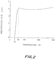
- resistivity-temperature characteristics of the thin oxide film were evaluated in a temperature region indicating the superconductive characteristics. The results are shown in Fig. 2.
- this first thin oxide film shows the onset of the superconductive transition at 60K and zero resistivity at 33K.
- Fig. 3 illustrates a X-ray diffraction pattern of the first thin oxide film.
- the abscissa represents an angle doubling the angle ⁇ of incidence of X-ray (2 ⁇ : unit: degrees) while the ordinate represents the intensity of the X-ray diffraction (unit: optional). It is to be noted that the measurement was made with 2 ⁇ lying within the range of 10° to 75°.
- the peaks P1, P2 and P3 represent diffraction peaks each corresponding to the SrTiO3 substrate 32. There also appear other peaks p1, p2 and p3 immediate to the right of the peaks P1, P2 and P3, respectively.
- the peak p1 (23.14°), p2 (47.21°), and p3 (73.79°) are diffraction peaks derived from (100) plane, (200) plane, and (300) plane of YBa2Cu3O x , respectively.
- the first thin oxide film has "a-axis" orientation.
- the lattice constant "a” is 3.85 angstrom. Therefore, the first thin oxide film shows superconductive characteristics, and includes a crystal structure comprising YBa2Cu3O x .
- This thin oxide film was formed by the use of a composite target consisting of the second target comprising the same constituent elements as the first target but in a different compositional ratio.
- the second target may be represented as YBa2Cu5O v (in the compositional ratio v is a value satisfying O ⁇ v with the upper limit undefined).
- This target is a sintered one.
- the second target designated at 28b used in lieu of the first target is placed on the cathode 24 in the same manner as the formation of the first thin oxide film.
- Film formation conditions to be employed at that time and film forming processes of the system are same as the formation conditions and the processes in the case of the first thin oxide film with the exception of changing the target cathode voltage. In this case, therefore, the switches 44a, 44b and 44c remain open (disconnecting state) so as to disconnect the external D.C. voltage sources 48a, 48b and 48c from their corresponding cathodes.
- the target cathode voltage employed in this embodiment was a self-bias voltage of minus 50 volts which is determined by sputtering conditions (such as the kind of sputtering gas to be used, sputtering gas pressure, discharge frequency, and input power) as well as system configuration (such as area ratio between the electrodes).
- the film formation rate of the second thin oxide film onto the (100) plane of the SrTiO3 substrate was 0.02 angstrom (which rate is one sixth of that of the first thin oxide film) with the film thickness of 400 angstrom.
- the formation of the second thin oxide film can be effected at a lower growth rate as described above under conditions of a relatively low self-bias voltage of about minus tens of volts and a relatively high pressure atmosphere of several hundred mTorr, which ensures an easier control of film thickness than is the case in the prior art. Consequently, the thickness of the second thin oxide film can be also controlled to lie under several ten angstrom.
- the resultant thin film is cooled down to room temperature under one atmospheric pressure oxygen followed by retrieval of the substrate 32 coated with the second thin oxide film.
- this second thin oxide film is represented as YBa2Cu3O y for the sake of convenience (y represents a component of the compositional ratio which is a value satisfying O ⁇ y with the upper limit undefined).
- the second thin oxide film that if the content of any one element among Y, Ba and Cu is employed as a basis of comparison, the contents of the other two elements lie within deviations of the order of 10% from the above compositional ratio.
- an oxide having a compositional ratio among Y, Ba and Cu of substantially equal to 1: 2: 3 generally presents superconductivity. It is therefore supposed that the present second thin oxide film also presents a superconductivity.
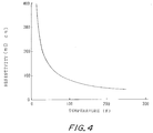
- the resistivity-temperature characteristics of the second thin oxide film were examined in the temperature range showing superconductivity.
- Fig. 4 illustrates the results.
- this second thin oxide film shows semiconductive characteristics at a relatively high temperature range and shows insulation characteristics at an extremely low temperature. In this manner, it has been found that the second thin oxide film is a substance showing both semiconductive characteristics and insulation characteristics depending on the temperature range, without showing superconductivity.
- Fig. 5 shows X-ray diffraction patterns of the second thin oxide film, and is similar to Fig. 3.
- the abscissa represents an angle doubling the angle of incidence of X-ray (2 ⁇ : unit: degrees) while the ordinate represents the intensity of X-ray diffraction (unit: optional). Note that this measurement was carried out within the range of 2 ⁇ lying 10° to 75°.
- peaks P4, P5 and P6 shows diffraction peaks each corresponding to SrTiO3 substrate 32. In this figure, there appear other peaks p4, p5 and p6 immediate to the right of the corresponding peaks P4, P5 and P6.
- peaks p4 (23.17°), p5 (47.34°) and p6 (73.98°) represent diffraction patterns, respectively derived from (100) plane, (200) plane and (300) plane of YBa2Cu3O x .
- this second thin oxide film includes crystals having "a-axis" orientation and a lattice constant "a" of 3.84 angstrom which is extremely close to the lattice constant 3.85 angstrom of the first thin oxide film. Based on this fact, the same deposition chamber can be used for a continuous formation of the first and second thin oxide films, thereby ensuring formation of the thin oxide film including a junction film consisting of both the films.
- FIG. 6 is a schematic sectional view of the thin oxide film 50.
- the first and second thin oxide films were formed under their respective film formation conditions which have been already described.
- the change-over switch 44a was closed (under connecting state) while disconnecting the other change-over switches 44b and 44c.
- the shutter facing the target 28a was opened while all the other shutters where closed.
- the switch 44a was disconnected, and simultaneously the turntable was rotated into a position where the substrate 32 faces the second target.
- the shutter facing the first target 28a was closed, and the shutter facing the second target 28b was opened to form the second thin oxide film 54 onto the first thin oxide film 52 which has been previously formed.
- the film formation conditions in this embodiment were the same as the previously described conditions in that the film thickness of the first thin oxide film 52 was 1000 angstrom, the film thickness of the second thin oxide film 54 was about 100 angstrom.
- the junction is designated at a reference numeral 56.
- the resistivity-temperature characteristics of the second thin oxide film 54 of the thin oxide film were measured by the D.C. 3-terminal method with the result that its behaviour is the same as the characteristics of the unitary film shown in Fig. 4 and that the second thin oxide film 54 itself presents both semiconductive characteristics and insulation characteristics depending on the temperature.
- the exposed surface of the second thin oxide film 54 was etched to a depth of about 500 angstrom toward the underlying first thin oxide film 52 with the aid of Ar (argon) ions, so that the first thin oxide film 52 is entirely exposed to measure the resistivity-temperature characteristics by the D.C. 4-terminal method. Consequently, the resistivity-temperature characteristics of the first thin oxide film 52 present the same behaviour as the characteristics of the unitary film shown in Fig. 2, that is, present superconductive characteristics.
- targets may be used and preferably include elements and a chemical composition which ensure that the first thin oxide film formed has a chemical composition represented as YBa2Cu3O z1 (note that the component z1 of the compositional ratio is a value satisfying O ⁇ z1) and that the second thin oxide film has a chemical composition represented as YBa2Cu3O z2 (note that the component z2 of the compositional ratio is a value satisfying O ⁇ z2) or a chemical compositional ratio close to that.
- the substrate is not limited to the SrTiO3 substrate merely employed by way of example. Any other substrate is applicable provided it is made of a material suitable for the film formation such as MgO and NdGaO3 so that the elements constituting the substrate and film do not undergo great interdiffusion between the substrate and the formed film.
- the film formation was effected by RF magnetron sputtering by way of example, but in other embodiments RF sputtering may be employed.
- first and second thin oxide films are intended to show a single junction between the first and second thin oxide films, but in other embodiments the formation of the first and second thin oxide films may be successively repeated in sequence to provide a thin oxide film having two or more junctions.
- the present invention uses the targets made of the same constituent elements to separately form a first thin oxide film and a second thin oxide film by changing only the voltage produced on the target cathode, the first thin oxide film showing superconductivity, and the second thin oxide film ordinarily showing semiconductive characteristics while being used as insulator in an extremely low temperature range, thus ensuring a successive film formation of the first and second thin oxide films in the same deposition chamber without any interruption of time.
- the thin oxide film which has been formed to include at least one junction is free from the mixture of contaminants into its junction interfacial area and from the formation of an area subject to a change in properties due to the contaminants. Therefore, the thin oxide film which has been formed in accordance with the present invention has a superior film quality and film characteristics as well as less possibility of deterioration in these characteristics as compared with conventional thin oxide film.
- the second thin oxide film does not show superconductivity even if the first thin oxide film is oxidized to impart superconductivity after the film formation.
- a couple of thin oxide films can be successively formed in the same deposition chamber with superior film quality and junction properties, and hence the present invention ensures a remarkably improved production efficiency of the thin oxide film as compared with conventional methods.
- the films resting on both sides of the junction have substantially the same lattice constant, and accordingly the lattice mismatching lessens, thus enabling an epitaxial growth of the semiconductor constituent material onto this thin oxide film.
- the thus formed thin oxide film is suitable for use in the formation of devices having superconductive characteristics such as Josephson elements or superconducting circuitry.
Landscapes
- Engineering & Computer Science (AREA)
- Chemical & Material Sciences (AREA)
- Ceramic Engineering (AREA)
- Manufacturing & Machinery (AREA)
- Physical Vapour Deposition (AREA)
- Superconductor Devices And Manufacturing Methods Thereof (AREA)
- Inorganic Compounds Of Heavy Metals (AREA)
- Superconductors And Manufacturing Methods Therefor (AREA)
- Crystals, And After-Treatments Of Crystals (AREA)
Applications Claiming Priority (2)
| Application Number | Priority Date | Filing Date | Title |
|---|---|---|---|
| JP300820/91 | 1991-11-15 | ||
| JP3300820A JP2698254B2 (ja) | 1991-11-15 | 1991-11-15 | 酸化物薄膜の成膜方法 |
Publications (3)
| Publication Number | Publication Date |
|---|---|
| EP0543585A2 true EP0543585A2 (fr) | 1993-05-26 |
| EP0543585A3 EP0543585A3 (fr) | 1993-06-02 |
| EP0543585B1 EP0543585B1 (fr) | 1997-04-16 |
Family
ID=17889502
Family Applications (1)
| Application Number | Title | Priority Date | Filing Date |
|---|---|---|---|
| EP92310407A Expired - Lifetime EP0543585B1 (fr) | 1991-11-15 | 1992-11-13 | Procédé pour la préparation d'un film d'oxyde |
Country Status (3)
| Country | Link |
|---|---|
| EP (1) | EP0543585B1 (fr) |
| JP (1) | JP2698254B2 (fr) |
| DE (1) | DE69219075T2 (fr) |
Cited By (1)
| Publication number | Priority date | Publication date | Assignee | Title |
|---|---|---|---|---|
| US11339467B2 (en) | 2019-07-09 | 2022-05-24 | Samsung Electronics Co., Ltd. | Sputtering apparatus and method for fabricating semiconductor device using the same |
Families Citing this family (1)
| Publication number | Priority date | Publication date | Assignee | Title |
|---|---|---|---|---|
| JP4458740B2 (ja) * | 2002-09-13 | 2010-04-28 | 株式会社アルバック | バイアススパッタ成膜方法及びバイアススパッタ成膜装置 |
Family Cites Families (12)
| Publication number | Priority date | Publication date | Assignee | Title |
|---|---|---|---|---|
| JPS63239990A (ja) * | 1987-03-27 | 1988-10-05 | Toshiba Corp | 超電導トランジスタ |
| JPS6411378A (en) * | 1987-07-06 | 1989-01-13 | Hitachi Ltd | Formation of josephson element |
| JPS6420639A (en) * | 1987-07-15 | 1989-01-24 | Sharp Kk | Manufacture of superconductor |
| JPS6451680A (en) * | 1987-08-22 | 1989-02-27 | Sumitomo Electric Industries | Oxide ceramics laminated layer structure and its manufacture |
| JPH01106479A (ja) * | 1987-10-20 | 1989-04-24 | Fujitsu Ltd | 超伝導材料構造 |
| JPH01140622A (ja) * | 1987-11-26 | 1989-06-01 | Taiyo Yuden Co Ltd | 超電導膜体を有する装置 |
| FR2626715B1 (fr) * | 1988-02-02 | 1990-05-18 | Thomson Csf | Dispositif en couches minces de materiau supraconducteur et procede de realisation |
| US4929595A (en) * | 1988-02-26 | 1990-05-29 | The University Of Alabama At Huntsville | Superconducting thin film fabrication |
| JPH02260674A (ja) * | 1989-03-31 | 1990-10-23 | Sumitomo Electric Ind Ltd | トンネル型ジョセフソン素子とその作製方法 |
| JP2814563B2 (ja) * | 1989-05-29 | 1998-10-22 | 住友電気工業株式会社 | 酸化物超電導膜の製造方法 |
| US5121173A (en) * | 1989-07-10 | 1992-06-09 | Santa Barbara Research Center | Proximity effect very long wavlength infrared (VLWIR) radiation detector |
| JP2588985B2 (ja) * | 1990-03-09 | 1997-03-12 | 財団法人国際超電導産業技術研究センター | 酸化物薄膜の成膜方法 |
-
1991
- 1991-11-15 JP JP3300820A patent/JP2698254B2/ja not_active Expired - Fee Related
-
1992
- 1992-11-13 EP EP92310407A patent/EP0543585B1/fr not_active Expired - Lifetime
- 1992-11-13 DE DE69219075T patent/DE69219075T2/de not_active Expired - Fee Related
Cited By (2)
| Publication number | Priority date | Publication date | Assignee | Title |
|---|---|---|---|---|
| US11339467B2 (en) | 2019-07-09 | 2022-05-24 | Samsung Electronics Co., Ltd. | Sputtering apparatus and method for fabricating semiconductor device using the same |
| US11725271B2 (en) | 2019-07-09 | 2023-08-15 | Samsung Electronics Co., Ltd. | Sputtering apparatus and method for fabricating semiconductor device using the same |
Also Published As
| Publication number | Publication date |
|---|---|
| DE69219075D1 (de) | 1997-05-22 |
| EP0543585B1 (fr) | 1997-04-16 |
| DE69219075T2 (de) | 1997-07-24 |
| JPH05139737A (ja) | 1993-06-08 |
| EP0543585A3 (fr) | 1993-06-02 |
| JP2698254B2 (ja) | 1998-01-19 |
Similar Documents
| Publication | Publication Date | Title |
|---|---|---|
| US4912087A (en) | Rapid thermal annealing of superconducting oxide precursor films on Si and SiO2 substrates | |
| US5169829A (en) | Method for producing a superconducting circuit | |
| US5047385A (en) | Method of forming superconducting YBa2 Cu3 O7-x thin films with controlled crystal orientation | |
| CN1022654C (zh) | 隧道型约瑟夫森器件及其制造方法 | |
| US5171732A (en) | Method of making a josephson junction | |
| EP0282839B1 (fr) | Couches d'oxydes supraconducteurs à hautes Tc et leur procédé de fabrication | |
| Wakana et al. | Improvement in reproducibility of multilayer and junction process for HTS SFQ circuits | |
| US5567673A (en) | Process of forming multilayered Tl-containing superconducting composites | |
| EP0543585B1 (fr) | Procédé pour la préparation d'un film d'oxyde | |
| US5747427A (en) | Process for forming a semiconductive thin film containing a junction | |
| CA2003850C (fr) | Procede de preparation d'un film supraconducteur de type perovskite | |
| EP0358545A2 (fr) | Procédé de fabrication de couches minces supraconductrices du type au thallium | |
| JP2713343B2 (ja) | 超電導回路の作製方法 | |
| WO1989003125A1 (fr) | Procede de production d'un circuit electrique contenant des diodes de josephson | |
| JPH05182911A (ja) | スパッタ装置 | |
| Truman et al. | Continued improvement of large area, in situ sputter deposition of superconducting YBCO thin films | |
| EP0624910A1 (fr) | Supraconducteur et procédé de fabrication | |
| EP0333513B1 (fr) | Oxyde supraconducteur | |
| Häuser et al. | Study of the Preparation and Properties of YBaCuO-Films | |
| JPH0714816B2 (ja) | 希土類元素を含む超電導酸化物薄膜の形成方法 | |
| EP0465325A2 (fr) | Procédé pour la préparation d'un film mince à supraconducteur d'oxyde | |
| JP2525852B2 (ja) | 超電導薄膜の作製方法 | |
| Lin et al. | Large-area growth of superconducting Y-Ba-Cu-O films by hot-wall sputtering method | |
| Liu | A novel computer-controlled single ion beam multi-target sputter deposition system for yttrium barium copper oxide high transition temperature superconducting thin films | |
| JPH05194095A (ja) | 薄膜電気伝導体の製造方法 |
Legal Events
| Date | Code | Title | Description |
|---|---|---|---|
| PUAI | Public reference made under article 153(3) epc to a published international application that has entered the european phase |
Free format text: ORIGINAL CODE: 0009012 |
|
| PUAL | Search report despatched |
Free format text: ORIGINAL CODE: 0009013 |
|
| AK | Designated contracting states |
Kind code of ref document: A2 Designated state(s): DE FR GB |
|
| AK | Designated contracting states |
Kind code of ref document: A3 Designated state(s): DE FR GB |
|
| 17P | Request for examination filed |
Effective date: 19931105 |
|
| 17Q | First examination report despatched |
Effective date: 19941227 |
|
| GRAG | Despatch of communication of intention to grant |
Free format text: ORIGINAL CODE: EPIDOS AGRA |
|
| GRAH | Despatch of communication of intention to grant a patent |
Free format text: ORIGINAL CODE: EPIDOS IGRA |
|
| GRAH | Despatch of communication of intention to grant a patent |
Free format text: ORIGINAL CODE: EPIDOS IGRA |
|
| GRAA | (expected) grant |
Free format text: ORIGINAL CODE: 0009210 |
|
| AK | Designated contracting states |
Kind code of ref document: B1 Designated state(s): DE FR GB |
|
| REF | Corresponds to: |
Ref document number: 69219075 Country of ref document: DE Date of ref document: 19970522 |
|
| ET | Fr: translation filed | ||
| PLBE | No opposition filed within time limit |
Free format text: ORIGINAL CODE: 0009261 |
|
| 26N | No opposition filed | ||
| REG | Reference to a national code |
Ref country code: GB Ref legal event code: 732E |
|
| REG | Reference to a national code |
Ref country code: GB Ref legal event code: IF02 |
|
| REG | Reference to a national code |
Ref country code: FR Ref legal event code: TQ Ref country code: FR Ref legal event code: RM |
|
| PGFP | Annual fee paid to national office [announced via postgrant information from national office to epo] |
Ref country code: FR Payment date: 20041105 Year of fee payment: 13 |
|
| PGFP | Annual fee paid to national office [announced via postgrant information from national office to epo] |
Ref country code: GB Payment date: 20041112 Year of fee payment: 13 |
|
| PGFP | Annual fee paid to national office [announced via postgrant information from national office to epo] |
Ref country code: DE Payment date: 20041210 Year of fee payment: 13 |
|
| PG25 | Lapsed in a contracting state [announced via postgrant information from national office to epo] |
Ref country code: GB Free format text: LAPSE BECAUSE OF NON-PAYMENT OF DUE FEES Effective date: 20051113 |
|
| PG25 | Lapsed in a contracting state [announced via postgrant information from national office to epo] |
Ref country code: DE Free format text: LAPSE BECAUSE OF NON-PAYMENT OF DUE FEES Effective date: 20060601 |
|
| GBPC | Gb: european patent ceased through non-payment of renewal fee |
Effective date: 20051113 |
|
| PG25 | Lapsed in a contracting state [announced via postgrant information from national office to epo] |
Ref country code: FR Free format text: LAPSE BECAUSE OF NON-PAYMENT OF DUE FEES Effective date: 20060731 |
|
| REG | Reference to a national code |
Ref country code: FR Ref legal event code: ST Effective date: 20060731 |