EP0544338A1 - Circuit amplificateur opérationnel à transistors MOS - Google Patents
Circuit amplificateur opérationnel à transistors MOS Download PDFInfo
- Publication number
- EP0544338A1 EP0544338A1 EP92120352A EP92120352A EP0544338A1 EP 0544338 A1 EP0544338 A1 EP 0544338A1 EP 92120352 A EP92120352 A EP 92120352A EP 92120352 A EP92120352 A EP 92120352A EP 0544338 A1 EP0544338 A1 EP 0544338A1
- Authority
- EP
- European Patent Office
- Prior art keywords
- signal
- voltage level
- amplifier circuit
- voltage
- operational amplifier
- Prior art date
- Legal status (The legal status is an assumption and is not a legal conclusion. Google has not performed a legal analysis and makes no representation as to the accuracy of the status listed.)
- Granted
Links
Images

Classifications
-
- H—ELECTRICITY
- H03—ELECTRONIC CIRCUITRY
- H03F—AMPLIFIERS
- H03F3/00—Amplifiers with only discharge tubes or only semiconductor devices as amplifying elements
- H03F3/45—Differential amplifiers
- H03F3/45071—Differential amplifiers with semiconductor devices only
- H03F3/45076—Differential amplifiers with semiconductor devices only characterised by the way of implementation of the active amplifying circuit in the differential amplifier
- H03F3/45179—Differential amplifiers with semiconductor devices only characterised by the way of implementation of the active amplifying circuit in the differential amplifier using MOSFET transistors as the active amplifying circuit
-
- H—ELECTRICITY
- H03—ELECTRONIC CIRCUITRY
- H03F—AMPLIFIERS
- H03F3/00—Amplifiers with only discharge tubes or only semiconductor devices as amplifying elements
- H03F3/30—Single-ended push-pull [SEPP] amplifiers; Phase-splitters therefor
- H03F3/3001—Single-ended push-pull [SEPP] amplifiers; Phase-splitters therefor with field-effect transistors
-
- H—ELECTRICITY
- H03—ELECTRONIC CIRCUITRY
- H03F—AMPLIFIERS
- H03F2200/00—Indexing scheme relating to amplifiers
- H03F2200/153—Feedback used to stabilise the amplifier
-
- H—ELECTRICITY
- H03—ELECTRONIC CIRCUITRY
- H03F—AMPLIFIERS
- H03F2203/00—Indexing scheme relating to amplifiers with only discharge tubes or only semiconductor devices as amplifying elements covered by H03F3/00
- H03F2203/30—Indexing scheme relating to single-ended push-pull [SEPP]; Phase-splitters therefor
- H03F2203/30006—Indexing scheme relating to single-ended push-pull [SEPP]; Phase-splitters therefor the push and the pull stages of the SEPP amplifier are both current mirrors
-
- H—ELECTRICITY
- H03—ELECTRONIC CIRCUITRY
- H03F—AMPLIFIERS
- H03F2203/00—Indexing scheme relating to amplifiers with only discharge tubes or only semiconductor devices as amplifying elements covered by H03F3/00
- H03F2203/30—Indexing scheme relating to single-ended push-pull [SEPP]; Phase-splitters therefor
- H03F2203/30018—A series coupled active resistor and capacitor are coupled in a feedback circuit of a SEPP amplifier
-
- H—ELECTRICITY
- H03—ELECTRONIC CIRCUITRY
- H03F—AMPLIFIERS
- H03F2203/00—Indexing scheme relating to amplifiers with only discharge tubes or only semiconductor devices as amplifying elements covered by H03F3/00
- H03F2203/45—Indexing scheme relating to differential amplifiers
- H03F2203/45224—One output of the differential amplifier being taken into consideration
-
- H—ELECTRICITY
- H03—ELECTRONIC CIRCUITRY
- H03F—AMPLIFIERS
- H03F2203/00—Indexing scheme relating to amplifiers with only discharge tubes or only semiconductor devices as amplifying elements covered by H03F3/00
- H03F2203/45—Indexing scheme relating to differential amplifiers
- H03F2203/45274—Level shifting stages are added to the differential amplifier at a position other than the one or more inputs of the dif amp
Definitions
- the present invention relates to an operational amplifier circuit, and in particular to an operational amplifier circuit suitably used for a MOS integrated circuit.
- MOS operational amplifiers have been widely used for adding and subtracting analog signals and so forth.
- a prior art reference "MOS Operational Amplifier Design A Tutorial Overview", IEEE Journal of Solid-State Circuits, VOL. SC-17, No. 6, December 1982, Pages 969 to 981, discloses a conventional MOS operational amplifier circuit.
- a typical MOS operational amplifier circuit is composed of a differential amplifier circuit, a level shift circuit and an output circuit.
- This operational amplifier circuit serves as an AB operational amplifier which applies a large current to a load connected to its output when a signal is delivered thereto, but decreases a current running through the output stage when no signal is delivered.
- the conventional MOS operational amplifier circuit sometimes delivers an output signal having a distortion in a transient zone in which one of two MOS FETs that constitute the output stage and are connected in series, is turned on from its turned off condition since this one of MOS FETs is normally turned on.
- the conventional MOS operational amplifier circuit applies a large current to a small output load resistor so as to generate an output signal at a power source voltage level. Accordingly, it raise a problem in that large scale integration with a high density is difficult since the ratio W/L (where W is gate width and L is gate length) of the MOS FETs which constitute the output stage should be large.
- An object of the present invention is to provide an operational amplifier circuit which can deliver an output waveform having a less distortion.
- the other object of the present invention is to provide an operational amplifier circuit which is suitable for an integrated circuit.
- the other object of the present invention is to provide an operational amplifier circuit which has less current consumption.
- the present invention provides an operational amplifier circuit comprising: a differential amplifier circuit for delivering a signal which is obtained by amplifying a difference in voltage level between two signals; a level shift circuit for shifting and delivering a voltage level of the signal delivered from the differential amplifier circuit; a first amplifier circuit for amplifying and delivering the signal delivered from the level shift circuit; a second amplifier circuit for amplifying a voltage level of the signal delivered from the differential amplifier circuit; and a CMOS output circuit whose state is controlled in accordance with voltage levels of the signals delivered from the first and second amplifier circuits.
- CMOS complementary metal oxide semiconductor
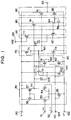
- This operational amplifier circuit comprises a differential amplifier circuit 50 for amplifying an input voltage applied to a normal phase input terminal 51 in accordance with a voltage difference between the normal phase input terminal 51 and a reverse phase input terminal 52, and then applying the thus amplified voltage to a node N1; a level shift circuit 60 for shifting the level of the voltage applied to the node N1 and then applying the thus shifted voltage to a node N2; a first amplifier circuit 70 for amplifying the voltage applied to the node N2 and then applying the same to a node N3, a second amplifier circuit 80 for amplifying the voltage applied to the node N1 and then applying the same to a node N4; an output circuit 90 connected to an output terminal, for applying an output voltage to the output terminal in accordance with the voltages applied to the nodes N3, N4, and a first and CMOS
- the first phase compensation circuit is composed of a first source follower circuit 100 and a capacitor 103, and controls the voltage at the node N1 in accordance with the voltage at the node N3 (through feed-back operation).
- the first source follower circuit 100 is connected between the node N1 and the node N3 through the intermediary of the capacitor 103 and comprises an NMOS transistor 101 and an NMOS transistor 102.
- the NMOS transistor 101 has a gate connected to the node N3, a drain connected to a positive power source terminal 120 and a source connected to a drain of the NMOS transistor 102. Further, the substrate of the NMOS transistor 101 is connected to the drain of the NMOS transistor 102.
- the NMOS transistor 102 has a gate connected to a bias terminal 124, a source connected to a negative power source terminal 122, and the drain connected to the source of the NMOS 101.
- the capacitor 103 is connected to the node N1 and the source of the NMOS transistor 101.
- the second phase compensation circuit 110 comprises a second source follower circuit 110 and a capacitor 113, and controls the voltage at the node N1 in accordance with the voltage at the node N4.
- the second source follower circuit 110 is connected between the nodes N1, N4 through the intermediary of the capacitor 113, and comprises PMOS transistors 111, 112.
- the PMOS transistors 111 has a gate connected to a bias terminal 126 applied with a bias voltage Vb2, a source connected to the positive power source terminal 120, and a drain connected to a source of the PMOS transistor 112.
- the PMOS transistor 112 has a gate connected to the node N4, a drain connected to the negative power source terminal 122, and the source connected to the drain of the PMOS transistor 111.
- capacitor 113 is connected to the node N1 and the source of the PMOS transistor 112.
- the differential amplifier circuit 50 is connected between the positive power source terminal 120 applied with a positive source power (+V) and the negative power source terminal 122 applied with a negative source power (-V), and comprises input NMOS transistors 53, 54, an NMOS transistor 55 constituting a low current source, PMOS transistors 56, 57 constituting a load.
- the NMOS transistor 53 has a gate connected to the normal phase input terminal 51, a drain connected to a drain of the PMOS transistor 56, and a source connected to a drain of the NMOS transistor 55.
- the NMOS transistor 54 has a gate connected to a reverse phase input terminal 52, a drain connected to a drain of the PMOS transistor 57 and a source connected to a drain of the NMOS transistor 55.
- the NMOS transistor 55 has a gate connected to the bias terminal 124 applied with a bias voltage Vb1, the drain connected commonly to the sources of the NMOS transistor 53 and the NMOS transistor 54, and a source connected to the negative power source terminal 122.
- the PMOS transistors 56, 57 have sources commonly connected to the positive power source terminal 120 and gates commonly connected to the drain of the NMOS transistor 53.
- the level shift circuit 60 is connected to the differential amplifier circuit 50, and comprises NMOS transistors 61, 62.
- the NMOS transistor 61 has a gate connected to the node N1, a drain connected to the positive power source terminal 120, and a source connected to the node N2. Further, the substrate of the NMOS transistor 61 is connected to the node N2.
- the NMOS transistor 62 has a gate connected to the bias terminal 124, a source connected to the negative power source terminal 122, and a drain connected to the node N2.
- the first amplifier circuit 70 is connected to the level shift circuit 60, and comprises PMOS transistors 71 and an NMOS transistor 72.
- the PMOS 71 has a source connected to the positive power source terminal 120, and a drain and a source connected to the node N3. Further, the PMOS transistor 71 serves as a load.
- the NMOS transistor 72 has a gate connected to the node N2, a gate connected to the negative power source terminal 122, and a drain connected to the node N3.
- the second amplifier circuit 80 is connected to the differential amplifier circuit 50, and comprises a PMOS transistor 81 and an NMOS transistor 82.
- the PMOS transistor 81 has a source connected to the positive power source terminal 120, and a drain connected to the node N4.
- the NMOS transistor 82 has a gate and a drain connected to the node N4, and a source connected to the negative power source terminal 122.
- the NMOS transistor 82 severs as a load.
- the output circuit 90 has a PMOS transistor 91 and an NMOS transistor 92.
- the PMOS transistor 91 has a gate connected to the node N3, a source connected to the positive power source terminal 120, and a drain connected to the output terminal 93.
- the NMOS transistor 92 has a gate connected to the node N4, a source connected to the negative power source terminal 122, and a drain connected to the output terminal 93.
- the PMOS transistor 91 has a threshold voltage which is equal to that of the PMOS transistor 71.
- the NMOS transistor 82 has a threshold voltage which is equal to that of the NMOS transistor 92.
- Fig. 2 is a view illustrating the relationship between signal waveforms at the nodes in the operational amplifier circuit according to the present invention, and potential level, and in which the ordinate exhibits voltage level and the abscissa exhibits signal waveform configuration at the nodes.
- the waveform configuration at each node is shown with a time t0 as a reference. It is estimated that the level of a signal applied to the reverse phase input terminal 52 is at a signal input midpoint.
- An input signal having a positive voltage level with respect to the reverse phase input terminal 52 (signal input midpoint potential level) is applied to the normal phase input terminal 51.
- This input signal is amplified and applied to the node N1 by the differential amplifier circuit 50 with the same phase as that of the input signal.
- the input signal applied to the node N1 is shifted in the positive direction by a degree corresponding to a variation in voltage at the node N1, and is applied to the node N2 by the level shift circuit 60. It is noted that the level shift circuit 50 has a voltage gain of 1, and accordingly, the input signal applied to the node N1 is not amplified thereby.
- the input signal applied to the node N2 and level-shifted is amplified by the first amplifier circuit 70 with a reverse phase by a degree corresponding to a variation in voltage at the node N2, and is then applied to the gate of the PMOS transistor 91 through the intermediary of the node N3. Then, the gate-source voltage of the PMOS transistor 91 becomes higher so that the PMOS transistor 91 is activated. Accordingly, a current from the power source is fed to the load connected to the output terminal 93.
- the voltage at the node N3 is impedance-converted by the first source follower circuit 100, and is then fed back to the node N1 through the intermediary of the capacitor 103. Accordingly, it is possible to surely prevent the operational amplifier circuit from oscillating.
- the input signal applied to the node N1 is amplified with reverse phase by a degree corresponding to a variation in voltage produced at the node N1, and is applied to the gate of the NMOS transistor 92 through the intermediary of the node N4 by the second amplifier circuit 80. Then, the gate-source voltage of the NMOS transistor 92 becomes lower so that the current at the drain of the NMOS transistor 92 decreases. However, since the NMOS transistor 82 is provided, the voltage at the node N4 is maintained at the threshold voltage inherent to the NMOS transistor 82. Accordingly, the NMOS transistor 92 having a characteristic the same as that of the NMOS transistor 82 is not completely turned off.
- An input signal having a negative voltage level with respect to the reverse phase input terminal 52 is applied to the normal phase input terminal 51 by the differential amplifier circuit 50.
- This input signal is amplified and is applied to the node N1 with the same phase as that of the input signal.
- the input signal applied the node N1 is amplified by the second amplifier circuit 80 by a degree corresponding to a variation in voltage produced at the node N1 with reverse phase, and is then applied to the gate of the NMOS transistor 92 through the intermediary of the node N4. Accordingly, the NMOS transistor 92 is activated, contrary to that mentioned above. Thus, it is possible to absorb a current from the load connected to the output terminal 93.
- the PMOS transistor 91 since the voltage at the node N3 increases, contrary to that mentioned above, the PMOS transistor 91 is turned off. However, since the PMOS transistor 71 is provided, the voltage at the node N3 is maintained at the threshold voltage inherent to the PMOS transistor 71. Accordingly, the PMOS transistor 91 having a characteristic the same as that of the PMOS transistor 71, is not completely turned off.
- the voltage at the node N4 is impedance-converted by the second source follower circuit 110, and is then fed back to the node N1 through the intermediary of the capacitor 113. Accordingly, it is possible to prevent the operational amplifier circuit from oscillating.
- the voltage applied to the output terminal 93 is shifted smoothly from the positive direction to the negative direction or from the negative direction to the positive direction since the voltages with which the PMOS transistor 91 and the NMOS transistor 92 constituting the output circuit 90 are not completely turned off, are applied to the gates of these transistors 91, 92, a distortion (crossover distortion) in the waveform produced at the output terminal 93 can be reduced.
- the operation amplifier circuit can have a large degree of integration. Further, it is possible to reduce current consumption at the time when no signal is inputted.
Landscapes
- Engineering & Computer Science (AREA)
- Power Engineering (AREA)
- Amplifiers (AREA)
Applications Claiming Priority (2)
| Application Number | Priority Date | Filing Date | Title |
|---|---|---|---|
| JP31493291A JP3320434B2 (ja) | 1991-11-28 | 1991-11-28 | 演算増幅回路 |
| JP314932/91 | 1991-11-28 |
Publications (2)
| Publication Number | Publication Date |
|---|---|
| EP0544338A1 true EP0544338A1 (fr) | 1993-06-02 |
| EP0544338B1 EP0544338B1 (fr) | 1997-03-26 |
Family
ID=18059388
Family Applications (1)
| Application Number | Title | Priority Date | Filing Date |
|---|---|---|---|
| EP92120352A Expired - Lifetime EP0544338B1 (fr) | 1991-11-28 | 1992-11-27 | Circuit amplificateur opérationnel à transistors MOS |
Country Status (4)
| Country | Link |
|---|---|
| US (1) | US5289058A (fr) |
| EP (1) | EP0544338B1 (fr) |
| JP (1) | JP3320434B2 (fr) |
| DE (1) | DE69218552T2 (fr) |
Cited By (6)
| Publication number | Priority date | Publication date | Assignee | Title |
|---|---|---|---|---|
| US5856749A (en) * | 1996-11-01 | 1999-01-05 | Burr-Brown Corporation | Stable output bias current circuitry and method for low-impedance CMOS output stage |
| EP0765029A3 (fr) * | 1995-09-20 | 1999-05-12 | Mitsubishi Denki Kabushiki Kaisha | Circuit amplificateur à amplificateur opérationnel CMOS |
| CN1067194C (zh) * | 1995-07-24 | 2001-06-13 | 摩托罗拉公司 | 适合于安装到衬底上的运算放大器输出级及其放大方法 |
| CN1084085C (zh) * | 1996-02-23 | 2002-05-01 | 冲电气工业株式会社 | 运算放大电路 |
| CN1088288C (zh) * | 1997-09-04 | 2002-07-24 | 日本电气株式会社 | 运算放大器 |
| CN1093338C (zh) * | 1994-02-21 | 2002-10-23 | 艾利森电话股份有限公司 | 信号接收和信号处理装置 |
Families Citing this family (13)
| Publication number | Priority date | Publication date | Assignee | Title |
|---|---|---|---|---|
| JPH05312850A (ja) * | 1992-05-12 | 1993-11-26 | Nec Ic Microcomput Syst Ltd | 半導体集積回路 |
| US5546047A (en) * | 1995-02-27 | 1996-08-13 | Motorola, Inc. | Method and apparatus of an operational amplifier with wide dynamic range |
| US5736874A (en) * | 1996-09-20 | 1998-04-07 | Lucent Technologies Inc. | High resolution high speed comparator |
| US5838191A (en) * | 1997-02-21 | 1998-11-17 | National Semiconductor Corporation | Bias circuit for switched capacitor applications |
| US6049253A (en) * | 1998-01-29 | 2000-04-11 | Matsushita Electric Industrial Co., Ltd. | Operational amplifier |
| JP3875392B2 (ja) * | 1998-02-23 | 2007-01-31 | 株式会社東芝 | 演算増幅器 |
| US6018267A (en) * | 1998-03-10 | 2000-01-25 | Information Storage Devices, Inc. | High output swing operational amplifier using low voltage devices |
| JP2000151291A (ja) * | 1998-11-12 | 2000-05-30 | Fujitsu Ltd | 演算増幅器 |
| US6127891A (en) * | 1999-04-05 | 2000-10-03 | National Semiconductor Corporation | Low voltage class AB amplifier with gain boosting |
| US6590453B2 (en) * | 2001-09-21 | 2003-07-08 | Silicon Storage Technology, Inc. | Folded cascode high voltage operational amplifier with class AB source follower output stage |
| EP1582418A1 (fr) * | 2004-03-30 | 2005-10-05 | Dialog Semiconductor GmbH | Appareil de contrôle pour un détonateur d'airbag |
| JP5128996B2 (ja) * | 2008-04-01 | 2013-01-23 | ラピスセミコンダクタ株式会社 | 出力回路、及びオフセットキャンセル方法 |
| CN101800519B (zh) * | 2009-02-09 | 2015-02-04 | 普诚科技股份有限公司 | 运算放大器及降低运算放大器的偏移电压的方法 |
Citations (4)
| Publication number | Priority date | Publication date | Assignee | Title |
|---|---|---|---|---|
| US4335355A (en) * | 1979-09-28 | 1982-06-15 | American Microsystems, Inc. | CMOS Operational amplifier with reduced power dissipation |
| US4480230A (en) * | 1983-07-05 | 1984-10-30 | National Semiconductor Corporation | Large swing CMOS power amplifier |
| EP0256729A2 (fr) * | 1986-08-13 | 1988-02-24 | Kabushiki Kaisha Toshiba | Circuit amplificateur |
| WO1988006379A1 (fr) * | 1987-02-20 | 1988-08-25 | Alcatel N.V. | Circuit correcteur pour amplificateurs |
Family Cites Families (1)
| Publication number | Priority date | Publication date | Assignee | Title |
|---|---|---|---|---|
| KR950007836B1 (ko) * | 1990-11-27 | 1995-07-20 | 삼성전자주식회사 | 시모스 파워 증폭기 |
-
1991
- 1991-11-28 JP JP31493291A patent/JP3320434B2/ja not_active Expired - Fee Related
-
1992
- 1992-11-24 US US07/980,771 patent/US5289058A/en not_active Expired - Lifetime
- 1992-11-27 DE DE69218552T patent/DE69218552T2/de not_active Expired - Fee Related
- 1992-11-27 EP EP92120352A patent/EP0544338B1/fr not_active Expired - Lifetime
Patent Citations (4)
| Publication number | Priority date | Publication date | Assignee | Title |
|---|---|---|---|---|
| US4335355A (en) * | 1979-09-28 | 1982-06-15 | American Microsystems, Inc. | CMOS Operational amplifier with reduced power dissipation |
| US4480230A (en) * | 1983-07-05 | 1984-10-30 | National Semiconductor Corporation | Large swing CMOS power amplifier |
| EP0256729A2 (fr) * | 1986-08-13 | 1988-02-24 | Kabushiki Kaisha Toshiba | Circuit amplificateur |
| WO1988006379A1 (fr) * | 1987-02-20 | 1988-08-25 | Alcatel N.V. | Circuit correcteur pour amplificateurs |
Non-Patent Citations (2)
| Title |
|---|
| IEEE JOURNAL OF SOLID-STATE CIRCUITS vol. 25, no. 1, February 1990, NEW YORK pages 265 - 273 OPTEYNDE ET AL 'A CMOS Large-Swing Low-Distortion Three-Stage Class AB Power Amplifier' * |
| IEEE JOURNAL OF SOLID-STATE CIRCUITS vol. SC-17, no. 6, December 1982, pages 969 - 982 GRAY ET AL 'MOS Operational Amplifier Design- A Tutorial Overview' * |
Cited By (7)
| Publication number | Priority date | Publication date | Assignee | Title |
|---|---|---|---|---|
| CN1093338C (zh) * | 1994-02-21 | 2002-10-23 | 艾利森电话股份有限公司 | 信号接收和信号处理装置 |
| CN1067194C (zh) * | 1995-07-24 | 2001-06-13 | 摩托罗拉公司 | 适合于安装到衬底上的运算放大器输出级及其放大方法 |
| EP0765029A3 (fr) * | 1995-09-20 | 1999-05-12 | Mitsubishi Denki Kabushiki Kaisha | Circuit amplificateur à amplificateur opérationnel CMOS |
| CN1084085C (zh) * | 1996-02-23 | 2002-05-01 | 冲电气工业株式会社 | 运算放大电路 |
| US5856749A (en) * | 1996-11-01 | 1999-01-05 | Burr-Brown Corporation | Stable output bias current circuitry and method for low-impedance CMOS output stage |
| US6002276A (en) * | 1996-11-01 | 1999-12-14 | Burr-Brown Corporation | Stable output bias current circuitry and method for low-impedance CMOS output stage |
| CN1088288C (zh) * | 1997-09-04 | 2002-07-24 | 日本电气株式会社 | 运算放大器 |
Also Published As
| Publication number | Publication date |
|---|---|
| EP0544338B1 (fr) | 1997-03-26 |
| JPH05152870A (ja) | 1993-06-18 |
| JP3320434B2 (ja) | 2002-09-03 |
| DE69218552T2 (de) | 1997-11-13 |
| US5289058A (en) | 1994-02-22 |
| DE69218552D1 (de) | 1997-04-30 |
Similar Documents
| Publication | Publication Date | Title |
|---|---|---|
| EP0544338B1 (fr) | Circuit amplificateur opérationnel à transistors MOS | |
| US5907259A (en) | Operational amplification circuit capable of driving a high load | |
| EP0256729B1 (fr) | Circuit amplificateur | |
| JP3181507B2 (ja) | スイッチドキャパシタを導入した低電圧差動増幅器のための装置 | |
| EP0037406B1 (fr) | Amplificateur operationnel a cmos avec dissipation de puissance reduite | |
| US4247824A (en) | Linear amplifier | |
| US4484148A (en) | Current source frequency compensation for a CMOS amplifier | |
| KR100275177B1 (ko) | 저전압차동증폭기 | |
| US6242980B1 (en) | Differential amplifier circuit | |
| KR960039566A (ko) | 차동증폭 및 출력오프셋회로와 이를 구비한 반도체집적회로 및 노이즈 제거방법 | |
| US4336503A (en) | Driver circuit having reduced cross-over distortion | |
| US6317000B1 (en) | Overload recovery circuit and method | |
| US5221910A (en) | Single-pin amplifier in integrated circuit form | |
| US6989716B2 (en) | Variable gain amplifier | |
| US6624696B1 (en) | Apparatus and method for a compact class AB turn-around stage with low noise, low offset, and low power consumption | |
| US4431971A (en) | Dynamic operational amplifier | |
| US6496066B2 (en) | Fully differential operational amplifier of the folded cascode type | |
| US12224724B2 (en) | Local common mode feedback resistor-based amplifier with overshoot mitigation | |
| US4333025A (en) | N-Channel MOS comparator | |
| US6175277B1 (en) | Bias network for CMOS power devices | |
| US7071772B2 (en) | Differential amplifier | |
| US20060181349A1 (en) | CMOS variable gain amplifier for controlling dB linear gain | |
| US7161431B2 (en) | Class B amplifier with process variation independent deadband | |
| JP2540767B2 (ja) | 差動増幅回路 | |
| EP0499645A1 (fr) | Circuit amplificateur differentiel dans un amplificateur operationnel |
Legal Events
| Date | Code | Title | Description |
|---|---|---|---|
| PUAI | Public reference made under article 153(3) epc to a published international application that has entered the european phase |
Free format text: ORIGINAL CODE: 0009012 |
|
| AK | Designated contracting states |
Kind code of ref document: A1 Designated state(s): DE FR NL |
|
| 17P | Request for examination filed |
Effective date: 19930812 |
|
| 17Q | First examination report despatched |
Effective date: 19950616 |
|
| GRAG | Despatch of communication of intention to grant |
Free format text: ORIGINAL CODE: EPIDOS AGRA |
|
| GRAH | Despatch of communication of intention to grant a patent |
Free format text: ORIGINAL CODE: EPIDOS IGRA |
|
| GRAH | Despatch of communication of intention to grant a patent |
Free format text: ORIGINAL CODE: EPIDOS IGRA |
|
| GRAA | (expected) grant |
Free format text: ORIGINAL CODE: 0009210 |
|
| AK | Designated contracting states |
Kind code of ref document: B1 Designated state(s): DE FR NL |
|
| REF | Corresponds to: |
Ref document number: 69218552 Country of ref document: DE Date of ref document: 19970430 |
|
| ET | Fr: translation filed | ||
| PLBE | No opposition filed within time limit |
Free format text: ORIGINAL CODE: 0009261 |
|
| STAA | Information on the status of an ep patent application or granted ep patent |
Free format text: STATUS: NO OPPOSITION FILED WITHIN TIME LIMIT |
|
| 26N | No opposition filed | ||
| PGFP | Annual fee paid to national office [announced via postgrant information from national office to epo] |
Ref country code: FR Payment date: 20011113 Year of fee payment: 10 |
|
| PGFP | Annual fee paid to national office [announced via postgrant information from national office to epo] |
Ref country code: NL Payment date: 20011129 Year of fee payment: 10 |
|
| PGFP | Annual fee paid to national office [announced via postgrant information from national office to epo] |
Ref country code: DE Payment date: 20011210 Year of fee payment: 10 |
|
| PG25 | Lapsed in a contracting state [announced via postgrant information from national office to epo] |
Ref country code: NL Free format text: LAPSE BECAUSE OF NON-PAYMENT OF DUE FEES Effective date: 20030601 |
|
| PG25 | Lapsed in a contracting state [announced via postgrant information from national office to epo] |
Ref country code: DE Free format text: LAPSE BECAUSE OF NON-PAYMENT OF DUE FEES Effective date: 20030603 |
|
| PG25 | Lapsed in a contracting state [announced via postgrant information from national office to epo] |
Ref country code: FR Free format text: LAPSE BECAUSE OF NON-PAYMENT OF DUE FEES Effective date: 20030731 |
|
| NLV4 | Nl: lapsed or anulled due to non-payment of the annual fee |
Effective date: 20030601 |
|
| REG | Reference to a national code |
Ref country code: FR Ref legal event code: ST |