EP0545183A1 - Circuit pour la production de séquences binaires pseudo-aléatoires - Google Patents
Circuit pour la production de séquences binaires pseudo-aléatoires Download PDFInfo
- Publication number
- EP0545183A1 EP0545183A1 EP92119864A EP92119864A EP0545183A1 EP 0545183 A1 EP0545183 A1 EP 0545183A1 EP 92119864 A EP92119864 A EP 92119864A EP 92119864 A EP92119864 A EP 92119864A EP 0545183 A1 EP0545183 A1 EP 0545183A1
- Authority
- EP
- European Patent Office
- Prior art keywords
- pseudo
- random sequences
- circuit arrangement
- modulo
- random
- Prior art date
- Legal status (The legal status is an assumption and is not a legal conclusion. Google has not performed a legal analysis and makes no representation as to the accuracy of the status listed.)
- Granted
Links
Images




Classifications
-
- H—ELECTRICITY
- H04—ELECTRIC COMMUNICATION TECHNIQUE
- H04L—TRANSMISSION OF DIGITAL INFORMATION, e.g. TELEGRAPHIC COMMUNICATION
- H04L25/00—Baseband systems
- H04L25/02—Details ; arrangements for supplying electrical power along data transmission lines
- H04L25/03—Shaping networks in transmitter or receiver, e.g. adaptive shaping networks
- H04L25/03828—Arrangements for spectral shaping; Arrangements for providing signals with specified spectral properties
- H04L25/03866—Arrangements for spectral shaping; Arrangements for providing signals with specified spectral properties using scrambling
- H04L25/03872—Parallel scrambling or descrambling
-
- G—PHYSICS
- G06—COMPUTING OR CALCULATING; COUNTING
- G06F—ELECTRIC DIGITAL DATA PROCESSING
- G06F7/00—Methods or arrangements for processing data by operating upon the order or content of the data handled
- G06F7/58—Random or pseudo-random number generators
- G06F7/582—Pseudo-random number generators
- G06F7/584—Pseudo-random number generators using finite field arithmetic, e.g. using a linear feedback shift register
-
- H—ELECTRICITY
- H04—ELECTRIC COMMUNICATION TECHNIQUE
- H04J—MULTIPLEX COMMUNICATION
- H04J2203/00—Aspects of optical multiplex systems other than those covered by H04J14/05 and H04J14/07
- H04J2203/0001—Provisions for broadband connections in integrated services digital network using frames of the Optical Transport Network [OTN] or using synchronous transfer mode [STM], e.g. SONET, SDH
- H04J2203/0089—Multiplexing, e.g. coding, scrambling, SONET
Definitions
- the invention relates to a circuit for generating binary pseudo-random sequences according to the preamble of claim 1 and a scrambler provided with such a circuit arrangement.
- the taps on individual memory cells of the shift register can be connected to a network.
- the tapped pseudo-random sequences are added to one another modulo-2 in logical combination elements, as a result of which further similar pseudo-random sequences are generated with a different phase delay.
- the invention is based on the object of creating a circuit arrangement for the parallel generation of similar, phase-shifted binary pseudo-random sequences in which the minimum clock period is independent of the number of modulo-2 additions to be carried out, for the generation of pseudo-random sequences with a certain phase delay, is.
- a circuit arrangement for the parallel generation of similar, phase-shifted binary pseudo-random sequences is used in a so-called scrambler.
- Scramblers are circuits that scramble an input data stream so that longer 0 or 1 sequences occur only with a low probability and the probability of occurrence of 0 and 1 is the same. They are mainly used to ensure sufficient edge changes in clock-regenerating circuits, but applications are also known where scramblers are used to encrypt data.
- Descramblers are circuits that restore the original data from the data scrambled by the scambler. Generators of pseudo-random sequences are used to generate test patterns which can be used, for example, for measurement and monitoring purposes in transmission facilities.
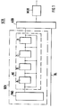
- An additive scrambler SCR contains a circuit arrangement SCH with a word generator PNG, which is followed by a network NE.
- the network NE consists of four parts A to D in which further pseudo-random sequences are generated from existing pseudo-random sequences and these further pseudo-random sequences are buffered for one clock period. In the next clock period, pseudo-random sequences are in turn generated in part from the temporarily stored pseudo-random sequences and / or passed to an output of the circuit arrangement SCH.
- a modulo-2 adder ADD the parallel pseudo-random sequences generated in the circuit arrangement SCH and the partial data streams also present in parallel on a data line DL are linked to one another and converted in a serial-to-multiplexer MUX.
- a pseudo-random sequence is generated in a feedback seven-stage shift register.
- the memory cells FF6 and FF7 in an exclusive OR gate EXOR1 (hereinafter referred to as EXOR gate) linked together and led to the input ESR of the shift register SR.
- EXOR1 exclusive OR gate
- D i is the input at the input, D6 the binary value in the memory cell FF6 and D7 the binary value in the memory cell FF7.
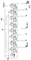
- the word generator PNG is constructed from seven D flip-flops FF1 to FF7 and an EXOR gate EXOR1.
- the D flip-flops represent the memory cells of the shift register SR and are each connected in series with one another via the Q outputs and the D inputs.
- the Q outputs of the D flip-flops FF6 and FF7 are guided to the inputs of the EXOR gate EXOR1 and connected to the D input of the first flip-flop FF1 via the output of the EXOR gate EXOR1.
- Via a set line SET the set inputs S of the flip-flops FF1 to FF7 can be set to 1.
- the invention is described using a scrambler which is provided for scrambling data streams which are constructed and transmitted according to the synchronous digital hierarchy SDH in accordance with CCITT recommendations G.707 to G.709.
- the scrambler is intended to scramble an STM-16 frame with a bit repetition frequency of 2.48832 Gbit / s.
- the scrambling takes place word by word for a 32 bit wide word at a word clock frequency of 77.76 MHz.
- the invention is particularly suitable for use in the abovementioned scrambler, but is not restricted to this use. Advantages in the use mentioned above are that, despite a high degree of parallelization, partial data streams can be scrambled with a high bit rate.
- the circuit arrangement SCH according to the invention can in principle also be used in a descrambler or in another device in which pseudo-random sequences are required.
- the circuit arrangement according to the invention can advantageously be implemented as a CMOS gate array, but is also suitable for implementation in any other technology, such as in GaAs technology.
- the word generator shown in FIG. 2 is intended for a serial, additive scrambler and generates a pseudo-random sequence in accordance with the CCITT recommendation G.709 2.4.
- a parallel additive scrambler it must be taken into account that a data stream to be scrambled is first converted into parallel partial data streams with a lower bit repetition frequency in a serial-parallel converter, and each partial data stream is scrambled separately and the entire scrambled partial data streams are converted in parallel in a multiplexer . It should be noted that the partial data stream that has now been serially converted must be scrambled in accordance with the Education Act of CCITT recommendation G.709 2.4.
- the serial data stream is converted from 32 parallel partial data streams by multiplexing in parallel-serial.
- two adjacent parallel partial data streams are each scrambled with a similar pseudo-random sequence, the pseudo-random sequences for two adjacent partial data streams being phase-shifted from one another by 4 bits.
- the serial data stream generated by multiplexing is scrambled in this way according to the CCITT recommendation mentioned above.
- the word generator PNG in the exemplary embodiment has a 7-stage shift register SR, which is constructed from D flip-flops, it is able to generate pseudo-random sequences with a length of 127 symbols.
- the word generator PNG of FIG. 2 produces 7 similar pseudo-random sequences in parallel, a first pseudo-random sequence being tapped at the output Q of the D flip-flop FF 1, which is referred to below as sequence No. 1. All phase shifts mentioned below are referred to as phase delay Ai, where i represents the delay in clock periods compared to sequence 1.
- the pseudo-random sequences applied to the outputs Q of the subsequent D flip-flops FF2 to FF7 each have a phase delay of one bit and, based on sequence 1, a phase delay A2 to A7. Due to the total length of a pseudo-random sequence of 127 bits, 127 similar pseudo-random sequences can be generated, as will be shown below. Table 1 shows the pseudo-random sequences present at the outputs Q of the D flip-flops FF1 to FF7 with the phase delays A0 to A6 over the total length of 127 bits or temporarily seen over a period of 127 clock cycles.
- sequences 2 to 31 the shift register SR is connected to a network NE as shown in FIGS. 3 to 6.
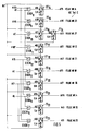
- the shift register SR of the word generator PNG from Fig. 1 is extended by a flip-flop FF8.
- the flip-flop FF8 cannot be functionally assigned to the word generator PNG, but rather represents part A of the network NE.
- the flip-flop FF als generates the sequence No. 31 as a clocked delay element with a phase delay A7, as can be seen in Table 2 is.
- the pending at the outputs Q of the flip-flops FF1 to FF7 are referred to below as pseudo-random sequences of the first generation.
- the sequence 31 already belongs to a group referred to below as the pseudo-random sequence of the second generation.
- the D-flip-flops FF1 to FF7 of the word generator PNG and the network NE are set as shown in FIGS. 3 to 6, that a set pulse applied via the set line SET generates a bit pattern from which the pseudo-random sequences listed in Table 2 with the phase relationship also shown in Table 2 arise. That is, if the set line SET is applied to the set input S, the corresponding D flip-flop FF becomes a logic 1 and if the set line is connected to the set pulse set input R of a D flip-flop, the flip-flop becomes a logic one 0 set.
- Part B consists of five exclusive OR gates EXOR3 to EXOR7 and five D flip-flops FF9 to FF13, which, as shown in Fig. 4, with each other, with the word generator PNG, part A and the parts C and described below D of the network NE are linked.
- Part C consists of 10 exclusive-OR gates EXOR8 to EXOR17 and 11 D flip-flops FF14 to FF24, as shown in Fig. 5 with each other, with the word generator PNG and the other parts A, B and D of the network NE are linked.
- a fourth generation of pseudo-random sequences the sequences No. 17, No. 30, No. 20, No. 16, No. 5, No. 24, No. 8, No. 19, No. 11, No. 7, No. 28, No. 29, No. 9 and No. 18 are generated in part D of the network shown in FIG. 6.
- Part D consists of 14 exclusive OR gates EXOR18 to EXOR31 and 15 D flip-flops FF25 to FF39, which are connected to each other and to the rest of the circuit arrangement as shown in Fig. 6.
- connections between the individual parts A, B, C and D of the network NE and the word generator PNG are given by the values Ai shown in the figures for the delay of the pseudo-random sequences applied to the respective connections.
- episodes of the third generation can be generated.
- sequences of other generations can be generated.
- four generations of random sequences have to be generated in order to obtain 32 phase-shifted pseudo-random sequences of the same type.
- modulo-2 additions In order to obtain a fourth generation pseudo-random sequence, up to three modulo-2 additions must be carried out. In the exemplary embodiment, this is done by leading an already existing pseudo-random sequence to the input of an exclusive-OR gate and adding modulo-2 with another pseudo-random sequence in this exclusive-OR gate. The result of the modulo 2 addition is buffered in a downstream D flip-flop.
- sequence 19 is described as an example of the generation of a fourth generation pseudo-random sequence.
- the sequences present at the outputs Q of the D flip-flops FF4 and FF mit with the delays A3 and A5 in the EXOR gate EXOR5 (part B) become a sequence of the second generation with a phase delay A118 in a first clock period modulo-2 added.
- the sequence with the delay A118 is cached in the D flip-flop FF11 and read out in a second clock period as a consequence with a delay A119, in the exclusive OR gate EXOR9 (part C) with a sequence of the delay A1, which comes directly from the Word generator PNG comes, modulo-2 added, which results in a sequence with delay A38.
- the sequence with the delay A38 is buffered in the D flip-flop FF15.
- a third clock period is at the output Q of the D flip-flop FF15 a sequence with the delay A39, from which, by modulo-2 addition with a sequence of the delay A23 in the exclusive OR gate EXOR25 (part D) one Consequence with the delay A54 of the third generation arises.
- the sequence with the delay A54 is written into the D flip-flop FF32.
- a pseudo-random sequence with the delay A55 is read out, this sequence represents the sequence No. 19 according to Table 2.
- two mechanisms are used to generate similar but phase-shifted pseudo-random sequences. Once a pseudo-random sequence is performed only using a delay element FF8, FF24 and FF39 and a delay of one bit is achieved. In the second case, modulo-2 addition of two pseudo-random sequences creates a pseudo-random sequence with a new phase position.
- the essence of the invention is that pseudo-random sequences generated by modulo-2 addition in the network NE are temporarily stored in a D-flip-flop FF8, ..., FF38 and thus to generate new random sequences of higher generations by modulo-2 Addition in the next cycle period are immediately available.
- intermediate generations of random sequences for example A54, A86, A102, A18, A14, A94, A58, must be generated. which then have the desired phase shift, for example A55, A87, A103, A19, A15, A95 and A59, only during the next clock period.
- the exemplary embodiment shown is designed in such a way that the cycle period is as short as possible, since only one modulo-2 addition is carried out in series during one cycle period.
- Applications are also conceivable in which it is advantageous to carry out two modulo-2 additions in series during a clock period. However, this would then result in a longer minimum clock period.
- the circuit arrangement SCH is connected to the outputs at which the sequences 1 to 32 are connected to 32 parallel exclusive-OR gates EXOR50 to EXOR81 of a modulo-2 adder ADD.
- the circuit arrangement SCH is supplemented to a parallel additive scrambler with a width of 32 bits.
- the modulo-2 adder ADD has 32 outputs OUT1 to OUT32, which are routed to the multiplexer MUX.
Landscapes
- Engineering & Computer Science (AREA)
- Physics & Mathematics (AREA)
- Theoretical Computer Science (AREA)
- General Physics & Mathematics (AREA)
- Mathematical Optimization (AREA)
- Pure & Applied Mathematics (AREA)
- Mathematical Analysis (AREA)
- General Engineering & Computer Science (AREA)
- Computational Mathematics (AREA)
- Spectroscopy & Molecular Physics (AREA)
- Power Engineering (AREA)
- Computer Networks & Wireless Communication (AREA)
- Signal Processing (AREA)
- Synchronisation In Digital Transmission Systems (AREA)
- Stereo-Broadcasting Methods (AREA)
- Detection And Prevention Of Errors In Transmission (AREA)
Applications Claiming Priority (2)
| Application Number | Priority Date | Filing Date | Title |
|---|---|---|---|
| DE4139630 | 1991-11-30 | ||
| DE4139630A DE4139630A1 (de) | 1991-11-30 | 1991-11-30 | Schaltungsanordnung zum erzeugen von binaeren pseudo-zufallsfolgen |
Publications (2)
| Publication Number | Publication Date |
|---|---|
| EP0545183A1 true EP0545183A1 (fr) | 1993-06-09 |
| EP0545183B1 EP0545183B1 (fr) | 1999-12-22 |
Family
ID=6446043
Family Applications (1)
| Application Number | Title | Priority Date | Filing Date |
|---|---|---|---|
| EP92119864A Expired - Lifetime EP0545183B1 (fr) | 1991-11-30 | 1992-11-21 | Circuit pour la production de séquences binaires pseudo-aléatoires |
Country Status (3)
| Country | Link |
|---|---|
| EP (1) | EP0545183B1 (fr) |
| AT (1) | ATE188047T1 (fr) |
| DE (2) | DE4139630A1 (fr) |
Families Citing this family (1)
| Publication number | Priority date | Publication date | Assignee | Title |
|---|---|---|---|---|
| DE102004022647B4 (de) * | 2004-05-07 | 2015-07-09 | Rohde & Schwarz Gmbh & Co. Kg | Verfahren und Vorrichtung zur Ermittlung der Anzahl von abgelaufenen Taktzyklen eines binären Zufallsgenerators |
Citations (3)
| Publication number | Priority date | Publication date | Assignee | Title |
|---|---|---|---|---|
| GB1591805A (en) * | 1978-01-12 | 1981-06-24 | Gen Electric Co Ltd | Electric signal generators |
| EP0150862A2 (fr) * | 1984-02-02 | 1985-08-07 | Siemens Aktiengesellschaft | Brouilleur auto-synchronisant |
| EP0301383A2 (fr) * | 1987-07-31 | 1989-02-01 | Advantest Corporation | Dispositif de génération d'une configuration pseudo-aléatoire |
-
1991
- 1991-11-30 DE DE4139630A patent/DE4139630A1/de not_active Withdrawn
-
1992
- 1992-11-21 DE DE59209784T patent/DE59209784D1/de not_active Expired - Fee Related
- 1992-11-21 EP EP92119864A patent/EP0545183B1/fr not_active Expired - Lifetime
- 1992-11-21 AT AT92119864T patent/ATE188047T1/de not_active IP Right Cessation
Patent Citations (3)
| Publication number | Priority date | Publication date | Assignee | Title |
|---|---|---|---|---|
| GB1591805A (en) * | 1978-01-12 | 1981-06-24 | Gen Electric Co Ltd | Electric signal generators |
| EP0150862A2 (fr) * | 1984-02-02 | 1985-08-07 | Siemens Aktiengesellschaft | Brouilleur auto-synchronisant |
| EP0301383A2 (fr) * | 1987-07-31 | 1989-02-01 | Advantest Corporation | Dispositif de génération d'une configuration pseudo-aléatoire |
Non-Patent Citations (1)
| Title |
|---|
| SIEMENS FORSCHUNGS- UND ENTWICKLUNGSBERICHTE Bd. 3, Nr. 4, 1974, BERLIN DE Seiten 218 - 224 K.H.M\RMANN 'ERZEUGUNG VON BIN[REN QUASI-ZUFALLSFOLGEN HOHER TAKTFREQUENZ DURCH MULTIPLEXEN' * |
Also Published As
| Publication number | Publication date |
|---|---|
| DE4139630A1 (de) | 1993-06-03 |
| EP0545183B1 (fr) | 1999-12-22 |
| DE59209784D1 (de) | 2000-01-27 |
| ATE188047T1 (de) | 2000-01-15 |
Similar Documents
| Publication | Publication Date | Title |
|---|---|---|
| DE2510278C2 (de) | Pseudozufalls-Wortgenerator | |
| EP2976707B1 (fr) | Dispositif et procédé pour générer des bits aléatoires | |
| DE69432587T2 (de) | Verzögerungsleitungsseparator für datenbus | |
| EP0553648B1 (fr) | Brouilleur et désembrouilleur parallèles | |
| DE68922930T2 (de) | Impulseinblendungsanordnung. | |
| DE2840552C2 (de) | Digitales Übertragungssystem | |
| DE3403650C2 (fr) | ||
| DE3420801C2 (fr) | ||
| DE3789819T2 (de) | Verarbeitungsschaltung für serielle Digitalsignale. | |
| DE3788783T2 (de) | Multiplexer für Taktsignale. | |
| EP0173842A2 (fr) | Débrouilleur autosynchronisant | |
| DE3722907A1 (de) | Maximallaengen-schieberegister-folgegenerator | |
| EP0150861B1 (fr) | Débrouilleur auto-synchronisant | |
| EP0257362A1 (fr) | Additionneur | |
| DE3131897A1 (de) | Steuersignal-multiplexschaltung | |
| EP0545183B1 (fr) | Circuit pour la production de séquences binaires pseudo-aléatoires | |
| DE4433512A1 (de) | Wellenform-Formatierungseinrichtung | |
| DE68918070T2 (de) | Digitales Übertragungssystem. | |
| DE4422784C2 (de) | Schaltungsanordnung mit wenigstens einer Schaltungseinheit wie einem Register, einer Speicherzelle, einer Speicheranordnung oder dergleichen | |
| DE2724110C2 (de) | Quasi-Zufallsgenerator | |
| DE2634353B1 (de) | Nachrichtenuebertragungssystem fuer pulscodemodulation mit sendeseitigem verwuerfler und synchronisiertem empfangsseitigem entwuerfler | |
| EP0197475B1 (fr) | Brouilleur et débrouilleur multiplicatif opérant par mots | |
| DE68923843T2 (de) | Synchroner logischer schaltkreis mit übertragungssignalsteuerung. | |
| DE10136575B4 (de) | Verfahren und Einrichtung zum Ausführen von Scramblermechanismen | |
| DE19619091A1 (de) | Hochgeschwindigkeits-Synchronzähler |
Legal Events
| Date | Code | Title | Description |
|---|---|---|---|
| PUAI | Public reference made under article 153(3) epc to a published international application that has entered the european phase |
Free format text: ORIGINAL CODE: 0009012 |
|
| AK | Designated contracting states |
Kind code of ref document: A1 Designated state(s): AT BE CH DE ES FR GB IT LI NL SE |
|
| 17P | Request for examination filed |
Effective date: 19930716 |
|
| 17Q | First examination report despatched |
Effective date: 19980730 |
|
| GRAG | Despatch of communication of intention to grant |
Free format text: ORIGINAL CODE: EPIDOS AGRA |
|
| GRAG | Despatch of communication of intention to grant |
Free format text: ORIGINAL CODE: EPIDOS AGRA |
|
| GRAH | Despatch of communication of intention to grant a patent |
Free format text: ORIGINAL CODE: EPIDOS IGRA |
|
| GRAH | Despatch of communication of intention to grant a patent |
Free format text: ORIGINAL CODE: EPIDOS IGRA |
|
| RAP1 | Party data changed (applicant data changed or rights of an application transferred) |
Owner name: ALCATEL |
|
| GRAA | (expected) grant |
Free format text: ORIGINAL CODE: 0009210 |
|
| AK | Designated contracting states |
Kind code of ref document: B1 Designated state(s): AT BE CH DE ES FR GB IT LI NL SE |
|
| PG25 | Lapsed in a contracting state [announced via postgrant information from national office to epo] |
Ref country code: SE Free format text: THE PATENT HAS BEEN ANNULLED BY A DECISION OF A NATIONAL AUTHORITY Effective date: 19991222 Ref country code: ES Free format text: THE PATENT HAS BEEN ANNULLED BY A DECISION OF A NATIONAL AUTHORITY Effective date: 19991222 Ref country code: NL Free format text: LAPSE BECAUSE OF FAILURE TO SUBMIT A TRANSLATION OF THE DESCRIPTION OR TO PAY THE FEE WITHIN THE PRESCRIBED TIME-LIMIT Effective date: 19991222 |
|
| REF | Corresponds to: |
Ref document number: 188047 Country of ref document: AT Date of ref document: 20000115 Kind code of ref document: T |
|
| ITF | It: translation for a ep patent filed | ||
| REG | Reference to a national code |
Ref country code: CH Ref legal event code: EP |
|
| GBT | Gb: translation of ep patent filed (gb section 77(6)(a)/1977) |
Effective date: 19991222 |
|
| REF | Corresponds to: |
Ref document number: 59209784 Country of ref document: DE Date of ref document: 20000127 |
|
| ET | Fr: translation filed | ||
| NLV1 | Nl: lapsed or annulled due to failure to fulfill the requirements of art. 29p and 29m of the patents act | ||
| PLBE | No opposition filed within time limit |
Free format text: ORIGINAL CODE: 0009261 |
|
| STAA | Information on the status of an ep patent application or granted ep patent |
Free format text: STATUS: NO OPPOSITION FILED WITHIN TIME LIMIT |
|
| PG25 | Lapsed in a contracting state [announced via postgrant information from national office to epo] |
Ref country code: AT Free format text: LAPSE BECAUSE OF NON-PAYMENT OF DUE FEES Effective date: 20001121 |
|
| PG25 | Lapsed in a contracting state [announced via postgrant information from national office to epo] |
Ref country code: LI Free format text: LAPSE BECAUSE OF NON-PAYMENT OF DUE FEES Effective date: 20001130 Ref country code: CH Free format text: LAPSE BECAUSE OF NON-PAYMENT OF DUE FEES Effective date: 20001130 Ref country code: BE Free format text: LAPSE BECAUSE OF NON-PAYMENT OF DUE FEES Effective date: 20001130 |
|
| 26N | No opposition filed | ||
| BERE | Be: lapsed |
Owner name: ALCATEL Effective date: 20001130 |
|
| REG | Reference to a national code |
Ref country code: CH Ref legal event code: PL |
|
| REG | Reference to a national code |
Ref country code: GB Ref legal event code: IF02 |
|
| PGFP | Annual fee paid to national office [announced via postgrant information from national office to epo] |
Ref country code: DE Payment date: 20071123 Year of fee payment: 16 |
|
| PGFP | Annual fee paid to national office [announced via postgrant information from national office to epo] |
Ref country code: IT Payment date: 20071126 Year of fee payment: 16 |
|
| PGFP | Annual fee paid to national office [announced via postgrant information from national office to epo] |
Ref country code: FR Payment date: 20071122 Year of fee payment: 16 Ref country code: GB Payment date: 20071120 Year of fee payment: 16 |
|
| GBPC | Gb: european patent ceased through non-payment of renewal fee |
Effective date: 20081121 |
|
| PG25 | Lapsed in a contracting state [announced via postgrant information from national office to epo] |
Ref country code: IT Free format text: LAPSE BECAUSE OF NON-PAYMENT OF DUE FEES Effective date: 20081121 |
|
| REG | Reference to a national code |
Ref country code: FR Ref legal event code: ST Effective date: 20090731 |
|
| PG25 | Lapsed in a contracting state [announced via postgrant information from national office to epo] |
Ref country code: DE Free format text: LAPSE BECAUSE OF NON-PAYMENT OF DUE FEES Effective date: 20090603 |
|
| PG25 | Lapsed in a contracting state [announced via postgrant information from national office to epo] |
Ref country code: GB Free format text: LAPSE BECAUSE OF NON-PAYMENT OF DUE FEES Effective date: 20081121 |
|
| PG25 | Lapsed in a contracting state [announced via postgrant information from national office to epo] |
Ref country code: FR Free format text: LAPSE BECAUSE OF NON-PAYMENT OF DUE FEES Effective date: 20081130 |