EP0546804A2 - Elektrischer Randverbinder - Google Patents
Elektrischer Randverbinder Download PDFInfo
- Publication number
- EP0546804A2 EP0546804A2 EP92311185A EP92311185A EP0546804A2 EP 0546804 A2 EP0546804 A2 EP 0546804A2 EP 92311185 A EP92311185 A EP 92311185A EP 92311185 A EP92311185 A EP 92311185A EP 0546804 A2 EP0546804 A2 EP 0546804A2
- Authority
- EP
- European Patent Office
- Prior art keywords
- housing
- circuit board
- board
- daughter board
- latch
- Prior art date
- Legal status (The legal status is an assumption and is not a legal conclusion. Google has not performed a legal analysis and makes no representation as to the accuracy of the status listed.)
- Granted
Links
Images

Classifications
-
- H—ELECTRICITY
- H01—ELECTRIC ELEMENTS
- H01R—ELECTRICALLY-CONDUCTIVE CONNECTIONS; STRUCTURAL ASSOCIATIONS OF A PLURALITY OF MUTUALLY-INSULATED ELECTRICAL CONNECTING ELEMENTS; COUPLING DEVICES; CURRENT COLLECTORS
- H01R9/00—Structural associations of a plurality of mutually-insulated electrical connecting elements, e.g. terminal strips or terminal blocks; Terminals or binding posts mounted upon a base or in a case; Bases therefor
-
- H—ELECTRICITY
- H01—ELECTRIC ELEMENTS
- H01R—ELECTRICALLY-CONDUCTIVE CONNECTIONS; STRUCTURAL ASSOCIATIONS OF A PLURALITY OF MUTUALLY-INSULATED ELECTRICAL CONNECTING ELEMENTS; COUPLING DEVICES; CURRENT COLLECTORS
- H01R12/00—Structural associations of a plurality of mutually-insulated electrical connecting elements, specially adapted for printed circuits, e.g. printed circuit boards [PCB], flat or ribbon cables, or like generally planar structures, e.g. terminal strips, terminal blocks; Coupling devices specially adapted for printed circuits, flat or ribbon cables, or like generally planar structures; Terminals specially adapted for contact with, or insertion into, printed circuits, flat or ribbon cables, or like generally planar structures
- H01R12/70—Coupling devices
- H01R12/71—Coupling devices for rigid printing circuits or like structures
- H01R12/72—Coupling devices for rigid printing circuits or like structures coupling with the edge of the rigid printed circuits or like structures
- H01R12/721—Coupling devices for rigid printing circuits or like structures coupling with the edge of the rigid printed circuits or like structures cooperating directly with the edge of the rigid printed circuits
Definitions
- the present invention relates to an electrical connector for electrically connecting together, for example, printed circuit boards.
- a daughter board such as a single-in-line memory module (SIMM)
- SIMM single-in-line memory module
- a mother board memory control board
- An electrical connector has a plastic housing mountable on a mother board.
- the housing has a slot into which the daughter board is inserted.
- the daughter board is connected to the mother board with the daughter board inserted in the slot of the housing. At this time, the daughter board has its attitude vertically fixed relative to the surface of the mother board. The daughter board thus fixed is electrically connected to those contact terminals arranged in the slot and placed in contact with the mother board.
- a pair of latch members are provided one at each end portion of the socket body such that they are integral with the socket body.
- the latch members are flexed in a direction to be moved by the daughter board away from each other, that is, are flexed outwardly of the socket body.
- the latch members are restored back to their initial configuration and the daughter board is sandwiched between the latch members.
- the daughter board is fixedly held at a vertical attitude.
- the latch members are outwardly flexed in a direction to be moved away from each other. It is thus possible to withdraw the daughter board out of engagement with the latch members.
- an electrical connector for connecting a first circuit board to a second circuit board comprising:
- the housing has a pair of guiding members for guiding the second circuit board to the recess, the pair of guiding member located in an opposed relation with the recess placed therebetween.
- the housing has a spring receiving cavity having an open lower end, the spring means being insertable into the spring receiving cavity though the lower end.
- the restricting member has a supporting portion for supporting the spring means positioned in the spring receiving cavity and the supporting portion extends along the open lower end of the spring receiving cavity and covers the open lower end.
- the latch member of the housing may has an area contacting with a lateral edge of the second circuit board, the latch member is tapered toward its base end at the contacting area.
- the latch member of the housing has a projection and the restricting member has a cutout engaging with the projection of the latch member.
- the flexing of the latch member is restricted by the restricting member, ensuring high durability of the latch member.
- a stable and strong holding force can be maintained even at the repetitive attachment and detachment of the second circuit board.
- a firm positive connection can be achieved between the first and second circuit boards by a mutual cooperation and coordination among the guide members, latch members and restricting members. It is possible to attach and detach the second circuit board to and from the socket body with a small force applied by a simple operation.
- latch members may molded integral with the housing as in the conventional counterpart structure and hence a simpler structure is employed, thus not only improving their durability but also lowering the manufacturing cost.
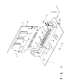
- an electrical connector 12 of the present invention is of such a type that a daughter board 2 is vertically connected to a mother board 1.
- the mother board 1 is comprised of, for example, a memory control board.
- the daughter board 2 is, for example, an SIMM (single-in-line memory module) on which memory chips 3 are mounted.
- a plurality of solder pads 5 are provided at a base end portion 4 of the daughter board 2 such that they are arranged in a direction of the width of the daughter board 2.
- a slit 6 is provided at a predetermined position at each side portion of the daughter board 2.
- the connector 12 has an elongated housing 14 molded of an elastic insulating material, such as plastics.
- a direction X denotes the longitudinal direction of the housing 14 and width direction of the daughter board 2;
- a direction Y the transverse direction of the housing 14;
- a direction Z the height direction of the housing 14.
- the housing 14 has a bottom surface 16 to be mounted on the mother board 1 and a top surface 18 on which the daughter board 2 is mounted.
- a leg 20 is provided at each end portion of the housing 14 and extends in the X-direction at that location where the housing 14 is mounted on the mother board 1.
- the legs 20 inserted through the mother board 1 are fixed in place by a soldering, etc., to allow an electrical connection to be done.
- a board-receiving opening 22 is provided along the X-direction in that top surface 18 of the housing 14 where the daughter board is mounted.
- a plurality of contact terminals 24 are arranged, as a row array, in the opening 22 along the X-direction.
- the contact terminals 24 can be arbitrarily selected from the known elastic contact terminals for circuit board (SIMM, etc.) connection.
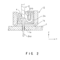
- the contacts 24 may be of such a type as indicated by a cross-sectional configuration in, for example, Fig. 2.
- the contacts 24 is electrically connected to the mother board 1 by a proper method for, for example, inserting one end portion 24a of the contacts 24 through a through hole 1 a of the mother board 1.
- a spring receiving cavity 26 is provided in the housing 14 at an area near each end of the board-receiving opening 22 and extends from the bottom surface of the opening 22 toward the bottom surface 16, noting that one end portion only of the opening 22 is shown for brevity's sake.
- a latch receiving cavity 28 is provided at each end side of the board-receiving opening 22.
- the cavity 28 extends through the housing 14 in the Z-direction and communicates with the opening 22 in the X-direction.
- the latch receiving cavity 28 communicates with the spring receiving cavity 26 via a recess 30 partially provided at the bottom surface 16 of the housing 14.
- a cover portion 58 of a reinforcing member 54 as will be set out below is so configured as to be fitted into the recess 30 of the housing 14.
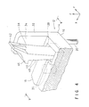
- a pair of guide arms 32 are molded integral with the housing 14 and arranged at each end portion of the top surface 18.
- the guide arms 32 have their opposed surfaces 34 and 36 in the Y direction with the latch receiving cavity 28 therebetween. Adistance between the opposed wall surfaces 34 and 36 corresponds to the width of the daughter board 2.
- a latch member 38 is located between the opposed wall surfaces 34 and 36 of the guide arms 32 and 32.
- the latch member 38 has its opposite side surfaces 40 and 40 provided integral with the opposed wall surfaces 34 and 36.
- Upper and lower ends 42 and 44 of the latch member 38 provided free ends.
- the lower end 44 of the latch member 38 is inserted into the latch member insertion hole 28.
- the opposed surfaces of the latch members 38 each, include a projection 46 engaging with the side slit 6 of the daughter board 2 and a support surface 48 to be abutted against a lateral edge 7 of the daughter board.
- the latch member 38 is elastically deformable in the X direction.
- the distance between the support surfaces 48 and 48 of the latch members 38 and 38 is made slightly smaller than the width W of the daughter board 2 so as to elastically hold both side edges 7 of the daughter board 2 between the support surfaces 48 and 48 of the latch members 38.
- the latch member 38 preferably has a grip 50 by which the daughter board 2 can be disengaged from the projections of the latch members.
- a rib 52 is projected on the outer surface of the grip 50.
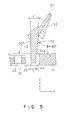
- the latch member 38 has its support surface 48 tapered as seen in cross-section.
- the X-direction width t of the latch member 38 at the lower end 44 of the support surface 48 is smaller than the X-direction width t' of the latch member38 at the upper end of the support surface 48.
- the support surface 48 of the latch member 38 is set at an angle of 90° to the top surface 18 and the latch member 38 has an outerwall surface 54a set an angle smaller than 90° to the top surface 18.
- a force acting to urgingly hold the daughter board in the X direction between the pair of latching members 38 and 38 is automatically produced at the top end portions of the latch members 38.
- the paired reinforcing metal plates 54 are provided one at each end side of the top surface 18 of the housing 14 and each fixedly inserted in the latch receiving cavity 28.
- the reinforcing metal plates 54 are arranged in an opposed relation in a manner to hold the latch members therebetween.
- the reinforcing metal plate 54 is L-shaped in cross-section and has a reinforcing section 56 abutted against the outer surface side of the latch member 38 and cover section 58 for covering the lower surface of the spring receiving cavity 26.
- the cover section 58 of the reinforcing metal plate 54 holds a coil spring 66, as will be set out below, against a slippage out of the housing 14.
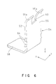
- the reinforcing section 56 of the reinforcing metal plate 54 reinforces the latch member 38 and, upon the attachment and detachment of the daughter board, restricts the latch member 38 against any undesired flexing.
- a cutout slit 60 is provided at the upper end portion of the reinforcing metal section 56 of the reinforcing metal plate 54 to engage with a rib 52 of the grip 50. Upon spreading the latch members 38 away from each other, the latch members 38 is restricted against any excessive flexing due to the rib 52 engaging with the slit 60 of the reinforcing metal sheet 54. It is thus possible to prevent a breakage of the latch member 38.
- a restricting member for restricting any excessive flexing of the latch member 38 can be provided by simply forming the cutout slit 60 at the plate-like reinforcing section 56 of the metal plate 56 located at the back of the latch member 36 in the X direction in which case the cutout slit 60 allows a displacement of the rib 52 resulting from the flexing of the latch member 38.
- the restricting member is simpler in its structure.
- the reinforcing metal sheet 54 restricts the latch member 38 from being flexed as set out above and does not serve to impart a supplementary holding force to the latch member 38 through the internal pushing of the latch member 38.
- the top end 56a of the reinforcing section 56 of the reinforcing metal plate 54 is desirably curved so as to prevent its edge from damaging the latch member as shown in the Figure.
- the cover section 56 of the reinforcing metal plate 54 is fitted into the recess 30 of the mother board mount surface 16 of the housing 14 and covers the lower side of the spring receiving cavity 26.
- the coil spring 66 inserted in the cavity 26 is placed on the upper surface of the cover section 58 of the metal plate 54.
- the daughter board 2 When daughter board 2 is to be mounted in the connector, the daughter board 2 is placed between the paired guide arms 32, 32 and 32, 32 with the base end 4 of the daughter board 2 down toward the board-receiving opening 22.
- the daughter board 2 is slidably moved along the guide arms 32 toward the contacts 14 until the solder pads 5 of the daughter board 4 are seated into electrical connection with the contacts 14 at the opening 22. At this time, the projections 46 of the latch members 38 are pushed by the daughter board 2 to allow the latch members to be moved away from each other, while being elastically deformed.
- the projections 46 of the latch members 38 are brought into engagement with the side slits 6 of the daughter board 2 and the latch member 38 is elastically restored back to its initial configuration.
- the support surfaces 48 of the latch members 38 are brought into abutting engagement with the lateral edges 7 of the daughter board to hold the daughter board 2 between the side surfaces of the latch members 38.
- the coil spring 6 is compressed by the base end of the daughter board, producing a spring force for pushing up the daughter board 2.
- the projection 46 of the latch member 38 is pushed against an upper edge 6a of the side slit 6 of the daughter board 2, urging the projection 46 into engagement with the slit it 6.
- the daughter board 2 is positively held in place. This ensures a positive electrical connection between the solder pads 5 of the daughter board 2 and the contacts 24.
- the latch members 38 Upon the detachment of the daughter board 2 from the connector 12, the latch members 38 are pushed away from each other. This operation is easier to do in the case where the handle 50 is provided integral with the latch member 38. This unlatches the daughter board 2 from the latch members 38. At this time, the daughter board 2 is pushed up under a vertical upward spring action of the coil spring 66 and ejected out of the contact terminals 24 and hence the opening 22. The unlatched daughter board 2 is pulled vertically out of the connector 12 until it is freely clear of the connector 12.
- the latch member 38 When the latch members 38 are deformed away from the housing 14 upon the attachment and detachment of the daughter board 2, the latch member 38 is restricted by the reinforcing metal plate 54 from being excessively flexed. This prevents a damage to the latch member 38 and ensures improved durability.
- the present invention is not restricted to the embodiment set out above and various changes or modifications of the present invention can be made.
- the daughter board 2 mounted on the socket has been explained as taking a vertical attitude relative to the mother board 4, it may be so mounted as to take a horizontal or an oblique attitude relative to the mother board.
- a plurality of board-receiving openings 22 may be provided in one housing 14 and a corresponding number of daughter boards 2 may be provided in one socket in which case latch members 38, reinforcing metal plates 54, coil springs 66, and so on, are provided in each opening 22.
Landscapes
- Coupling Device And Connection With Printed Circuit (AREA)
- Details Of Connecting Devices For Male And Female Coupling (AREA)
Applications Claiming Priority (2)
| Application Number | Priority Date | Filing Date | Title |
|---|---|---|---|
| JP3324611A JPH05159829A (ja) | 1991-12-09 | 1991-12-09 | 電気ソケット |
| JP324611/91 | 1991-12-09 |
Publications (3)
| Publication Number | Publication Date |
|---|---|
| EP0546804A2 true EP0546804A2 (de) | 1993-06-16 |
| EP0546804A3 EP0546804A3 (en) | 1993-09-08 |
| EP0546804B1 EP0546804B1 (de) | 1996-05-01 |
Family
ID=18167754
Family Applications (1)
| Application Number | Title | Priority Date | Filing Date |
|---|---|---|---|
| EP92311185A Expired - Lifetime EP0546804B1 (de) | 1991-12-09 | 1992-12-08 | Elektrischer Randverbinder |
Country Status (7)
| Country | Link |
|---|---|
| US (1) | US5413497A (de) |
| EP (1) | EP0546804B1 (de) |
| JP (1) | JPH05159829A (de) |
| KR (1) | KR950012748B1 (de) |
| DE (1) | DE69210365T2 (de) |
| SG (1) | SG46247A1 (de) |
| TW (1) | TW224548B (de) |
Cited By (9)
| Publication number | Priority date | Publication date | Assignee | Title |
|---|---|---|---|---|
| EP0797276A3 (de) * | 1996-03-21 | 1998-07-15 | Molex Incorporated | Verbinder mit verstärkter Verriegelung |
| EP0878035A4 (de) * | 1995-07-06 | 1998-11-18 | ||
| US5938463A (en) * | 1995-07-06 | 1999-08-17 | Berg Technology, Inc. | Socket for printed circuit boards |
| GB2336043A (en) * | 1998-01-29 | 1999-10-06 | Whitaker Corp | Retention device for processor module |
| AT406107B (de) * | 1997-09-22 | 2000-02-25 | Siemens Ag Oesterreich | Befestigungselement für zumindest eine zusatzleiterplatte auf einer mutterleiterplatte |
| DE19841467A1 (de) * | 1998-09-10 | 2000-04-13 | Siemens Ag | Platinen-Steckkontakt-Anordnung |
| EP1073150A3 (de) * | 1999-07-26 | 2001-05-02 | Berg Electronics Manufacturing B.V. | Steckbuchse für gedruckte Leiterplatte |
| US6497580B2 (en) * | 2000-03-01 | 2002-12-24 | Yazaki Corporation | Connector and a connecting structure of circuit boards therewith |
| GB2378821A (en) * | 2001-08-17 | 2003-02-19 | Hewlett Packard Co | Daughter-card to mother-board attachment |
Families Citing this family (30)
| Publication number | Priority date | Publication date | Assignee | Title |
|---|---|---|---|---|
| US5697802A (en) * | 1994-12-15 | 1997-12-16 | I-Pex Co., Ltd. | Electrical connector |
| JP3462920B2 (ja) * | 1994-12-21 | 2003-11-05 | バーグ・テクノロジー・インコーポレーテッド | プリント基板用ソケット |
| US6276950B1 (en) | 1994-12-21 | 2001-08-21 | Berg Technology, Inc. | Socket for printed circuit board |
| JP3015081U (ja) * | 1995-01-20 | 1995-08-29 | モレックス インコーポレーテッド | 印刷回路基板状体接続用電気コネクタ |
| US5784263A (en) * | 1996-01-08 | 1998-07-21 | Intel Corporation | Connector with attachable daughter card retention system |
| US5791925A (en) * | 1996-06-28 | 1998-08-11 | Berg Technology, Inc. | Card edge connector |
| US5689405A (en) * | 1996-09-25 | 1997-11-18 | Itt Corporation | IC card rear board support |
| JP3376221B2 (ja) * | 1996-10-02 | 2003-02-10 | ヒロセ電機株式会社 | 電気コネクタ |
| US6948956B2 (en) * | 2003-05-28 | 2005-09-27 | Fci Americas Technology, Inc. | Electrical connector with module ejection system |
| US6848921B2 (en) | 2003-05-28 | 2005-02-01 | Fci Americas Technology, Inc. | Electrical connector with module ejection system |
| US7029307B1 (en) * | 2004-12-14 | 2006-04-18 | Intel Corporation | Systems and methods for an improved card-edge connector |
| US7252523B1 (en) * | 2006-08-18 | 2007-08-07 | Tyco Electronics Corporation | Socket connector having latch biasing member |
| CN201041843Y (zh) * | 2007-03-09 | 2008-03-26 | 富士康(昆山)电脑接插件有限公司 | 电连接器 |
| CN201041840Y (zh) * | 2007-03-09 | 2008-03-26 | 富士康(昆山)电脑接插件有限公司 | 卡缘连接器 |
| TWI343154B (en) * | 2007-10-22 | 2011-06-01 | Asustek Comp Inc | Electronic device and connector and card insertion method thereof |
| CN201303139Y (zh) * | 2008-10-27 | 2009-09-02 | 富士康(昆山)电脑接插件有限公司 | 卡缘连接器 |
| DE102008054385A1 (de) * | 2008-12-08 | 2010-06-10 | Robert Bosch Gmbh | Elektrische Schaltungsanordnung, Steuergerät und Verfahren zum Herstellen einer elektrischen Schaltungsanordnung |
| JP2010225466A (ja) * | 2009-03-24 | 2010-10-07 | Fujitsu Component Ltd | 基板接続用コネクタ |
| US7883350B2 (en) * | 2009-04-29 | 2011-02-08 | Molex Incorporated | Header connectors with rigid latches |
| US20110171846A1 (en) * | 2010-01-11 | 2011-07-14 | Dell Products L.P. | Circuit Card Latching Arm Arresting Apparatus |
| US8369094B2 (en) * | 2010-05-19 | 2013-02-05 | Fujitsu Limited | Unibody latch for plug-in units |
| CN202025875U (zh) * | 2011-01-07 | 2011-11-02 | 美国莫列斯股份有限公司 | 卡缘连接器 |
| JP5510433B2 (ja) * | 2011-06-29 | 2014-06-04 | 第一精工株式会社 | 電気コネクタ |
| TWI513565B (zh) | 2011-10-19 | 2015-12-21 | Kunshan yurong electronics co ltd | 具加熱裝置的模具 |
| US8636528B2 (en) * | 2012-04-27 | 2014-01-28 | International Business Machines Corporation | Memory module connector with latch assist |
| DE102014101665A1 (de) * | 2014-02-11 | 2015-08-13 | Phoenix Contact Gmbh & Co. Kg | Elektrische Leiterplattensteckverbindung |
| CN105449454B (zh) * | 2014-08-07 | 2018-03-06 | 富士康(昆山)电脑接插件有限公司 | 卡缘连接器 |
| TWM515256U (zh) * | 2015-08-05 | 2016-01-01 | Nextronics Engineering Corp | 機箱面板的助拔裝置 |
| TW202017266A (zh) * | 2018-08-02 | 2020-05-01 | 美商山姆科技公司 | 收發器閂鎖與熱橋 |
| US12238883B2 (en) * | 2021-08-30 | 2025-02-25 | Penn Engineering & Manufacturing Corp. | Daughter-card retention system |
Family Cites Families (7)
| Publication number | Priority date | Publication date | Assignee | Title |
|---|---|---|---|---|
| US3823367A (en) * | 1973-09-04 | 1974-07-09 | Mallory & Co Inc P R | Battery package with end of life condition indicator |
| US4084874A (en) * | 1977-06-27 | 1978-04-18 | Gte Automatic Electric Laboratories Incorporated | Low insertion force connector |
| US4737120A (en) * | 1986-11-12 | 1988-04-12 | Amp Incorporated | Electrical connector with low insertion force and overstress protection |
| JP2570286B2 (ja) * | 1987-03-31 | 1997-01-08 | 三菱電機株式会社 | Icカ−ドコネクタ |
| US5226833A (en) * | 1991-08-23 | 1993-07-13 | E. I. Du Pont De Nemours And Company | Electrical connector |
| US5242312A (en) * | 1992-05-14 | 1993-09-07 | Robinson Nugent, Inc. | Board to socket retainer clip |
| US5203714A (en) * | 1992-06-18 | 1993-04-20 | Kenny Tuan | Electrical connector for a printed circuit board |
-
1991
- 1991-12-09 JP JP3324611A patent/JPH05159829A/ja active Pending
-
1992
- 1992-12-08 DE DE69210365T patent/DE69210365T2/de not_active Expired - Fee Related
- 1992-12-08 EP EP92311185A patent/EP0546804B1/de not_active Expired - Lifetime
- 1992-12-08 SG SG1996001599A patent/SG46247A1/en unknown
- 1992-12-09 KR KR1019920023675A patent/KR950012748B1/ko not_active Expired - Fee Related
- 1992-12-09 US US07/987,835 patent/US5413497A/en not_active Expired - Fee Related
- 1992-12-15 TW TW081110052A patent/TW224548B/zh active
Cited By (12)
| Publication number | Priority date | Publication date | Assignee | Title |
|---|---|---|---|---|
| EP0878035A4 (de) * | 1995-07-06 | 1998-11-18 | ||
| US5938463A (en) * | 1995-07-06 | 1999-08-17 | Berg Technology, Inc. | Socket for printed circuit boards |
| EP0797276A3 (de) * | 1996-03-21 | 1998-07-15 | Molex Incorporated | Verbinder mit verstärkter Verriegelung |
| AT406107B (de) * | 1997-09-22 | 2000-02-25 | Siemens Ag Oesterreich | Befestigungselement für zumindest eine zusatzleiterplatte auf einer mutterleiterplatte |
| GB2336043A (en) * | 1998-01-29 | 1999-10-06 | Whitaker Corp | Retention device for processor module |
| GB2336043B (en) * | 1998-01-29 | 2002-06-19 | Whitaker Corp | Retention device for processor module |
| DE19841467A1 (de) * | 1998-09-10 | 2000-04-13 | Siemens Ag | Platinen-Steckkontakt-Anordnung |
| EP1073150A3 (de) * | 1999-07-26 | 2001-05-02 | Berg Electronics Manufacturing B.V. | Steckbuchse für gedruckte Leiterplatte |
| US6527576B1 (en) | 1999-07-26 | 2003-03-04 | Berg Technology, Inc. | Socket for a printed board |
| US6497580B2 (en) * | 2000-03-01 | 2002-12-24 | Yazaki Corporation | Connector and a connecting structure of circuit boards therewith |
| GB2378821A (en) * | 2001-08-17 | 2003-02-19 | Hewlett Packard Co | Daughter-card to mother-board attachment |
| GB2378821B (en) * | 2001-08-17 | 2005-07-27 | Hewlett Packard Co | Daughter-card structural support |
Also Published As
| Publication number | Publication date |
|---|---|
| KR930015188A (ko) | 1993-07-24 |
| US5413497A (en) | 1995-05-09 |
| EP0546804B1 (de) | 1996-05-01 |
| JPH05159829A (ja) | 1993-06-25 |
| TW224548B (de) | 1994-06-01 |
| DE69210365T2 (de) | 1996-09-19 |
| SG46247A1 (en) | 1998-02-20 |
| HK1000396A1 (en) | 1998-03-13 |
| KR950012748B1 (ko) | 1995-10-20 |
| DE69210365D1 (de) | 1996-06-05 |
| EP0546804A3 (en) | 1993-09-08 |
Similar Documents
| Publication | Publication Date | Title |
|---|---|---|
| US5413497A (en) | Electrical connector | |
| EP0519264B1 (de) | Elektrischer Verbinder | |
| US5199895A (en) | Low insertion force, self-locking connecting apparatus for electrically connecting memory modules to a printed circuit board | |
| US20040005794A1 (en) | Construction for mounting a terminal, a circuit board connector and method of mounting it | |
| US6957967B2 (en) | Electrical connector with different pitch terminals | |
| US5046972A (en) | Low insertion force connector and contact | |
| US6955554B2 (en) | Electrical connector assembly having board hold down | |
| JPH0665101B2 (ja) | ソケット型電気コネクタ | |
| JP2002530822A (ja) | ガイド部材および取外しリセスを有する噛み合い電気コネクタアセンブリ | |
| EP0535965B1 (de) | Elektrischer Randverbindersockel | |
| JPH07509342A (ja) | フラットバックカードコネクタ | |
| US5226833A (en) | Electrical connector | |
| US7077678B1 (en) | Electrical connector assembly having board hold down | |
| US5154627A (en) | Electrical connector insertably fixed with simplified metal latches | |
| US6030243A (en) | Plug connector for card-edge mounting | |
| US5588861A (en) | ZIF chip socket | |
| US20020111064A1 (en) | Bottom entry connector | |
| JPH0587861U (ja) | 電気コネクタ | |
| EP0886349B1 (de) | Einseitiger Leiterplattenverbinder mit Gabelmontage | |
| HK1000396B (en) | Electrical connector | |
| US6478598B1 (en) | Electrical connector having improved contacts | |
| JPH0523429U (ja) | 表面実装型コネクタ | |
| JP3142901B2 (ja) | コネクタ装置 | |
| JPH0620744A (ja) | コネクタ装置 | |
| EP0878035B1 (de) | Fassung gedruckter leiterplatten |
Legal Events
| Date | Code | Title | Description |
|---|---|---|---|
| PUAI | Public reference made under article 153(3) epc to a published international application that has entered the european phase |
Free format text: ORIGINAL CODE: 0009012 |
|
| AK | Designated contracting states |
Kind code of ref document: A2 Designated state(s): DE FR GB |
|
| PUAL | Search report despatched |
Free format text: ORIGINAL CODE: 0009013 |
|
| AK | Designated contracting states |
Kind code of ref document: A3 Designated state(s): DE FR GB |
|
| 17P | Request for examination filed |
Effective date: 19931013 |
|
| 17Q | First examination report despatched |
Effective date: 19950116 |
|
| RAP1 | Party data changed (applicant data changed or rights of an application transferred) |
Owner name: CONNECTOR SYSTEMS TECHNOLOGY N.V. |
|
| GRAH | Despatch of communication of intention to grant a patent |
Free format text: ORIGINAL CODE: EPIDOS IGRA |
|
| GRAA | (expected) grant |
Free format text: ORIGINAL CODE: 0009210 |
|
| RAP1 | Party data changed (applicant data changed or rights of an application transferred) |
Owner name: BERG ELECTRONICS MANUFACTURING B.V. Owner name: CONNECTOR SYSTEMS TECHNOLOGY N.V. |
|
| AK | Designated contracting states |
Kind code of ref document: B1 Designated state(s): DE FR GB |
|
| REF | Corresponds to: |
Ref document number: 69210365 Country of ref document: DE Date of ref document: 19960605 |
|
| ET | Fr: translation filed | ||
| PLBE | No opposition filed within time limit |
Free format text: ORIGINAL CODE: 0009261 |
|
| 26N | No opposition filed | ||
| REG | Reference to a national code |
Ref country code: GB Ref legal event code: 732E |
|
| PGFP | Annual fee paid to national office [announced via postgrant information from national office to epo] |
Ref country code: GB Payment date: 19991112 Year of fee payment: 8 |
|
| PGFP | Annual fee paid to national office [announced via postgrant information from national office to epo] |
Ref country code: FR Payment date: 19991202 Year of fee payment: 8 |
|
| PGFP | Annual fee paid to national office [announced via postgrant information from national office to epo] |
Ref country code: DE Payment date: 19991222 Year of fee payment: 8 |
|
| PG25 | Lapsed in a contracting state [announced via postgrant information from national office to epo] |
Ref country code: GB Free format text: LAPSE BECAUSE OF NON-PAYMENT OF DUE FEES Effective date: 20001208 |
|
| GBPC | Gb: european patent ceased through non-payment of renewal fee |
Effective date: 20001208 |
|
| PG25 | Lapsed in a contracting state [announced via postgrant information from national office to epo] |
Ref country code: FR Free format text: LAPSE BECAUSE OF NON-PAYMENT OF DUE FEES Effective date: 20010831 |
|
| REG | Reference to a national code |
Ref country code: FR Ref legal event code: ST |
|
| PG25 | Lapsed in a contracting state [announced via postgrant information from national office to epo] |
Ref country code: DE Free format text: LAPSE BECAUSE OF NON-PAYMENT OF DUE FEES Effective date: 20011002 |