EP0547043B1 - Dispositif laser à semi-conducteur - Google Patents
Dispositif laser à semi-conducteur Download PDFInfo
- Publication number
- EP0547043B1 EP0547043B1 EP93200588A EP93200588A EP0547043B1 EP 0547043 B1 EP0547043 B1 EP 0547043B1 EP 93200588 A EP93200588 A EP 93200588A EP 93200588 A EP93200588 A EP 93200588A EP 0547043 B1 EP0547043 B1 EP 0547043B1
- Authority
- EP
- European Patent Office
- Prior art keywords
- type
- layer
- quantum well
- designates
- reference numeral
- Prior art date
- Legal status (The legal status is an assumption and is not a legal conclusion. Google has not performed a legal analysis and makes no representation as to the accuracy of the status listed.)
- Expired - Lifetime
Links
Images



Classifications
-
- H—ELECTRICITY
- H01—ELECTRIC ELEMENTS
- H01S—DEVICES USING THE PROCESS OF LIGHT AMPLIFICATION BY STIMULATED EMISSION OF RADIATION [LASER] TO AMPLIFY OR GENERATE LIGHT; DEVICES USING STIMULATED EMISSION OF ELECTROMAGNETIC RADIATION IN WAVE RANGES OTHER THAN OPTICAL
- H01S5/00—Semiconductor lasers
- H01S5/06—Arrangements for controlling the laser output parameters, e.g. by operating on the active medium
- H01S5/0601—Arrangements for controlling the laser output parameters, e.g. by operating on the active medium comprising an absorbing region
-
- B—PERFORMING OPERATIONS; TRANSPORTING
- B82—NANOTECHNOLOGY
- B82Y—SPECIFIC USES OR APPLICATIONS OF NANOSTRUCTURES; MEASUREMENT OR ANALYSIS OF NANOSTRUCTURES; MANUFACTURE OR TREATMENT OF NANOSTRUCTURES
- B82Y20/00—Nanooptics, e.g. quantum optics or photonic crystals
-
- H—ELECTRICITY
- H01—ELECTRIC ELEMENTS
- H01S—DEVICES USING THE PROCESS OF LIGHT AMPLIFICATION BY STIMULATED EMISSION OF RADIATION [LASER] TO AMPLIFY OR GENERATE LIGHT; DEVICES USING STIMULATED EMISSION OF ELECTROMAGNETIC RADIATION IN WAVE RANGES OTHER THAN OPTICAL
- H01S5/00—Semiconductor lasers
- H01S5/06—Arrangements for controlling the laser output parameters, e.g. by operating on the active medium
- H01S5/062—Arrangements for controlling the laser output parameters, e.g. by operating on the active medium by varying the potential of the electrodes
- H01S5/06209—Arrangements for controlling the laser output parameters, e.g. by operating on the active medium by varying the potential of the electrodes in single-section lasers
- H01S5/0622—Controlling the frequency of the radiation
-
- H—ELECTRICITY
- H01—ELECTRIC ELEMENTS
- H01S—DEVICES USING THE PROCESS OF LIGHT AMPLIFICATION BY STIMULATED EMISSION OF RADIATION [LASER] TO AMPLIFY OR GENERATE LIGHT; DEVICES USING STIMULATED EMISSION OF ELECTROMAGNETIC RADIATION IN WAVE RANGES OTHER THAN OPTICAL
- H01S5/00—Semiconductor lasers
- H01S5/10—Construction or shape of the optical resonator, e.g. extended or external cavity, coupled cavities, bent-guide, varying width, thickness or composition of the active region
-
- H—ELECTRICITY
- H01—ELECTRIC ELEMENTS
- H01S—DEVICES USING THE PROCESS OF LIGHT AMPLIFICATION BY STIMULATED EMISSION OF RADIATION [LASER] TO AMPLIFY OR GENERATE LIGHT; DEVICES USING STIMULATED EMISSION OF ELECTROMAGNETIC RADIATION IN WAVE RANGES OTHER THAN OPTICAL
- H01S5/00—Semiconductor lasers
- H01S5/10—Construction or shape of the optical resonator, e.g. extended or external cavity, coupled cavities, bent-guide, varying width, thickness or composition of the active region
- H01S5/12—Construction or shape of the optical resonator, e.g. extended or external cavity, coupled cavities, bent-guide, varying width, thickness or composition of the active region the resonator having a periodic structure, e.g. in distributed feedback [DFB] lasers
-
- H—ELECTRICITY
- H01—ELECTRIC ELEMENTS
- H01S—DEVICES USING THE PROCESS OF LIGHT AMPLIFICATION BY STIMULATED EMISSION OF RADIATION [LASER] TO AMPLIFY OR GENERATE LIGHT; DEVICES USING STIMULATED EMISSION OF ELECTROMAGNETIC RADIATION IN WAVE RANGES OTHER THAN OPTICAL
- H01S5/00—Semiconductor lasers
- H01S5/30—Structure or shape of the active region; Materials used for the active region
- H01S5/34—Structure or shape of the active region; Materials used for the active region comprising quantum well or superlattice structures, e.g. single quantum well [SQW] lasers, multiple quantum well [MQW] lasers or graded index separate confinement heterostructure [GRINSCH] lasers
-
- H—ELECTRICITY
- H01—ELECTRIC ELEMENTS
- H01S—DEVICES USING THE PROCESS OF LIGHT AMPLIFICATION BY STIMULATED EMISSION OF RADIATION [LASER] TO AMPLIFY OR GENERATE LIGHT; DEVICES USING STIMULATED EMISSION OF ELECTROMAGNETIC RADIATION IN WAVE RANGES OTHER THAN OPTICAL
- H01S5/00—Semiconductor lasers
- H01S5/40—Arrangement of two or more semiconductor lasers, not provided for in groups H01S5/02 - H01S5/30
- H01S5/4025—Array arrangements, e.g. constituted by discrete laser diodes or laser bar
- H01S5/4031—Edge-emitting structures
-
- H—ELECTRICITY
- H01—ELECTRIC ELEMENTS
- H01S—DEVICES USING THE PROCESS OF LIGHT AMPLIFICATION BY STIMULATED EMISSION OF RADIATION [LASER] TO AMPLIFY OR GENERATE LIGHT; DEVICES USING STIMULATED EMISSION OF ELECTROMAGNETIC RADIATION IN WAVE RANGES OTHER THAN OPTICAL
- H01S5/00—Semiconductor lasers
- H01S5/02—Structural details or components not essential to laser action
- H01S5/028—Coatings ; Treatment of the laser facets, e.g. etching, passivation layers or reflecting layers
-
- H—ELECTRICITY
- H01—ELECTRIC ELEMENTS
- H01S—DEVICES USING THE PROCESS OF LIGHT AMPLIFICATION BY STIMULATED EMISSION OF RADIATION [LASER] TO AMPLIFY OR GENERATE LIGHT; DEVICES USING STIMULATED EMISSION OF ELECTROMAGNETIC RADIATION IN WAVE RANGES OTHER THAN OPTICAL
- H01S5/00—Semiconductor lasers
- H01S5/06—Arrangements for controlling the laser output parameters, e.g. by operating on the active medium
-
- H—ELECTRICITY
- H01—ELECTRIC ELEMENTS
- H01S—DEVICES USING THE PROCESS OF LIGHT AMPLIFICATION BY STIMULATED EMISSION OF RADIATION [LASER] TO AMPLIFY OR GENERATE LIGHT; DEVICES USING STIMULATED EMISSION OF ELECTROMAGNETIC RADIATION IN WAVE RANGES OTHER THAN OPTICAL
- H01S5/00—Semiconductor lasers
- H01S5/06—Arrangements for controlling the laser output parameters, e.g. by operating on the active medium
- H01S5/0601—Arrangements for controlling the laser output parameters, e.g. by operating on the active medium comprising an absorbing region
- H01S5/0602—Arrangements for controlling the laser output parameters, e.g. by operating on the active medium comprising an absorbing region which is an umpumped part of the active layer
-
- H—ELECTRICITY
- H01—ELECTRIC ELEMENTS
- H01S—DEVICES USING THE PROCESS OF LIGHT AMPLIFICATION BY STIMULATED EMISSION OF RADIATION [LASER] TO AMPLIFY OR GENERATE LIGHT; DEVICES USING STIMULATED EMISSION OF ELECTROMAGNETIC RADIATION IN WAVE RANGES OTHER THAN OPTICAL
- H01S5/00—Semiconductor lasers
- H01S5/06—Arrangements for controlling the laser output parameters, e.g. by operating on the active medium
- H01S5/062—Arrangements for controlling the laser output parameters, e.g. by operating on the active medium by varying the potential of the electrodes
- H01S5/06203—Transistor-type lasers
- H01S5/06206—Controlling the frequency of the radiation, e.g. tunable twin-guide lasers [TTG]
-
- H—ELECTRICITY
- H01—ELECTRIC ELEMENTS
- H01S—DEVICES USING THE PROCESS OF LIGHT AMPLIFICATION BY STIMULATED EMISSION OF RADIATION [LASER] TO AMPLIFY OR GENERATE LIGHT; DEVICES USING STIMULATED EMISSION OF ELECTROMAGNETIC RADIATION IN WAVE RANGES OTHER THAN OPTICAL
- H01S5/00—Semiconductor lasers
- H01S5/06—Arrangements for controlling the laser output parameters, e.g. by operating on the active medium
- H01S5/062—Arrangements for controlling the laser output parameters, e.g. by operating on the active medium by varying the potential of the electrodes
- H01S5/06209—Arrangements for controlling the laser output parameters, e.g. by operating on the active medium by varying the potential of the electrodes in single-section lasers
- H01S5/06213—Amplitude modulation
-
- H—ELECTRICITY
- H01—ELECTRIC ELEMENTS
- H01S—DEVICES USING THE PROCESS OF LIGHT AMPLIFICATION BY STIMULATED EMISSION OF RADIATION [LASER] TO AMPLIFY OR GENERATE LIGHT; DEVICES USING STIMULATED EMISSION OF ELECTROMAGNETIC RADIATION IN WAVE RANGES OTHER THAN OPTICAL
- H01S5/00—Semiconductor lasers
- H01S5/06—Arrangements for controlling the laser output parameters, e.g. by operating on the active medium
- H01S5/062—Arrangements for controlling the laser output parameters, e.g. by operating on the active medium by varying the potential of the electrodes
- H01S5/0625—Arrangements for controlling the laser output parameters, e.g. by operating on the active medium by varying the potential of the electrodes in multi-section lasers
- H01S5/06255—Controlling the frequency of the radiation
-
- H—ELECTRICITY
- H01—ELECTRIC ELEMENTS
- H01S—DEVICES USING THE PROCESS OF LIGHT AMPLIFICATION BY STIMULATED EMISSION OF RADIATION [LASER] TO AMPLIFY OR GENERATE LIGHT; DEVICES USING STIMULATED EMISSION OF ELECTROMAGNETIC RADIATION IN WAVE RANGES OTHER THAN OPTICAL
- H01S5/00—Semiconductor lasers
- H01S5/06—Arrangements for controlling the laser output parameters, e.g. by operating on the active medium
- H01S5/062—Arrangements for controlling the laser output parameters, e.g. by operating on the active medium by varying the potential of the electrodes
- H01S5/0625—Arrangements for controlling the laser output parameters, e.g. by operating on the active medium by varying the potential of the electrodes in multi-section lasers
- H01S5/06255—Controlling the frequency of the radiation
- H01S5/06258—Controlling the frequency of the radiation with DFB-structure
-
- H—ELECTRICITY
- H01—ELECTRIC ELEMENTS
- H01S—DEVICES USING THE PROCESS OF LIGHT AMPLIFICATION BY STIMULATED EMISSION OF RADIATION [LASER] TO AMPLIFY OR GENERATE LIGHT; DEVICES USING STIMULATED EMISSION OF ELECTROMAGNETIC RADIATION IN WAVE RANGES OTHER THAN OPTICAL
- H01S5/00—Semiconductor lasers
- H01S5/10—Construction or shape of the optical resonator, e.g. extended or external cavity, coupled cavities, bent-guide, varying width, thickness or composition of the active region
- H01S5/1039—Details on the cavity length
-
- H—ELECTRICITY
- H01—ELECTRIC ELEMENTS
- H01S—DEVICES USING THE PROCESS OF LIGHT AMPLIFICATION BY STIMULATED EMISSION OF RADIATION [LASER] TO AMPLIFY OR GENERATE LIGHT; DEVICES USING STIMULATED EMISSION OF ELECTROMAGNETIC RADIATION IN WAVE RANGES OTHER THAN OPTICAL
- H01S5/00—Semiconductor lasers
- H01S5/10—Construction or shape of the optical resonator, e.g. extended or external cavity, coupled cavities, bent-guide, varying width, thickness or composition of the active region
- H01S5/12—Construction or shape of the optical resonator, e.g. extended or external cavity, coupled cavities, bent-guide, varying width, thickness or composition of the active region the resonator having a periodic structure, e.g. in distributed feedback [DFB] lasers
- H01S5/1206—Construction or shape of the optical resonator, e.g. extended or external cavity, coupled cavities, bent-guide, varying width, thickness or composition of the active region the resonator having a periodic structure, e.g. in distributed feedback [DFB] lasers having a non constant or multiplicity of periods
- H01S5/1215—Multiplicity of periods
-
- H—ELECTRICITY
- H01—ELECTRIC ELEMENTS
- H01S—DEVICES USING THE PROCESS OF LIGHT AMPLIFICATION BY STIMULATED EMISSION OF RADIATION [LASER] TO AMPLIFY OR GENERATE LIGHT; DEVICES USING STIMULATED EMISSION OF ELECTROMAGNETIC RADIATION IN WAVE RANGES OTHER THAN OPTICAL
- H01S5/00—Semiconductor lasers
- H01S5/10—Construction or shape of the optical resonator, e.g. extended or external cavity, coupled cavities, bent-guide, varying width, thickness or composition of the active region
- H01S5/12—Construction or shape of the optical resonator, e.g. extended or external cavity, coupled cavities, bent-guide, varying width, thickness or composition of the active region the resonator having a periodic structure, e.g. in distributed feedback [DFB] lasers
- H01S5/1228—DFB lasers with a complex coupled grating, e.g. gain or loss coupling
-
- H—ELECTRICITY
- H01—ELECTRIC ELEMENTS
- H01S—DEVICES USING THE PROCESS OF LIGHT AMPLIFICATION BY STIMULATED EMISSION OF RADIATION [LASER] TO AMPLIFY OR GENERATE LIGHT; DEVICES USING STIMULATED EMISSION OF ELECTROMAGNETIC RADIATION IN WAVE RANGES OTHER THAN OPTICAL
- H01S5/00—Semiconductor lasers
- H01S5/10—Construction or shape of the optical resonator, e.g. extended or external cavity, coupled cavities, bent-guide, varying width, thickness or composition of the active region
- H01S5/12—Construction or shape of the optical resonator, e.g. extended or external cavity, coupled cavities, bent-guide, varying width, thickness or composition of the active region the resonator having a periodic structure, e.g. in distributed feedback [DFB] lasers
- H01S5/125—Distributed Bragg reflector [DBR] lasers
-
- H—ELECTRICITY
- H01—ELECTRIC ELEMENTS
- H01S—DEVICES USING THE PROCESS OF LIGHT AMPLIFICATION BY STIMULATED EMISSION OF RADIATION [LASER] TO AMPLIFY OR GENERATE LIGHT; DEVICES USING STIMULATED EMISSION OF ELECTROMAGNETIC RADIATION IN WAVE RANGES OTHER THAN OPTICAL
- H01S5/00—Semiconductor lasers
- H01S5/20—Structure or shape of the semiconductor body to guide the optical wave ; Confining structures perpendicular to the optical axis, e.g. index or gain guiding, stripe geometry, broad area lasers, gain tailoring, transverse or lateral reflectors, special cladding structures, MQW barrier reflection layers
-
- H—ELECTRICITY
- H01—ELECTRIC ELEMENTS
- H01S—DEVICES USING THE PROCESS OF LIGHT AMPLIFICATION BY STIMULATED EMISSION OF RADIATION [LASER] TO AMPLIFY OR GENERATE LIGHT; DEVICES USING STIMULATED EMISSION OF ELECTROMAGNETIC RADIATION IN WAVE RANGES OTHER THAN OPTICAL
- H01S5/00—Semiconductor lasers
- H01S5/20—Structure or shape of the semiconductor body to guide the optical wave ; Confining structures perpendicular to the optical axis, e.g. index or gain guiding, stripe geometry, broad area lasers, gain tailoring, transverse or lateral reflectors, special cladding structures, MQW barrier reflection layers
- H01S5/2004—Confining in the direction perpendicular to the layer structure
-
- H—ELECTRICITY
- H01—ELECTRIC ELEMENTS
- H01S—DEVICES USING THE PROCESS OF LIGHT AMPLIFICATION BY STIMULATED EMISSION OF RADIATION [LASER] TO AMPLIFY OR GENERATE LIGHT; DEVICES USING STIMULATED EMISSION OF ELECTROMAGNETIC RADIATION IN WAVE RANGES OTHER THAN OPTICAL
- H01S5/00—Semiconductor lasers
- H01S5/20—Structure or shape of the semiconductor body to guide the optical wave ; Confining structures perpendicular to the optical axis, e.g. index or gain guiding, stripe geometry, broad area lasers, gain tailoring, transverse or lateral reflectors, special cladding structures, MQW barrier reflection layers
- H01S5/2004—Confining in the direction perpendicular to the layer structure
- H01S5/2009—Confining in the direction perpendicular to the layer structure by using electron barrier layers
-
- H—ELECTRICITY
- H01—ELECTRIC ELEMENTS
- H01S—DEVICES USING THE PROCESS OF LIGHT AMPLIFICATION BY STIMULATED EMISSION OF RADIATION [LASER] TO AMPLIFY OR GENERATE LIGHT; DEVICES USING STIMULATED EMISSION OF ELECTROMAGNETIC RADIATION IN WAVE RANGES OTHER THAN OPTICAL
- H01S5/00—Semiconductor lasers
- H01S5/30—Structure or shape of the active region; Materials used for the active region
- H01S5/32—Structure or shape of the active region; Materials used for the active region comprising PN junctions, e.g. hetero- or double- heterostructures
- H01S5/3211—Structure or shape of the active region; Materials used for the active region comprising PN junctions, e.g. hetero- or double- heterostructures characterised by special cladding layers, e.g. details on band-discontinuities
- H01S5/3216—Structure or shape of the active region; Materials used for the active region comprising PN junctions, e.g. hetero- or double- heterostructures characterised by special cladding layers, e.g. details on band-discontinuities quantum well or superlattice cladding layers
-
- H—ELECTRICITY
- H01—ELECTRIC ELEMENTS
- H01S—DEVICES USING THE PROCESS OF LIGHT AMPLIFICATION BY STIMULATED EMISSION OF RADIATION [LASER] TO AMPLIFY OR GENERATE LIGHT; DEVICES USING STIMULATED EMISSION OF ELECTROMAGNETIC RADIATION IN WAVE RANGES OTHER THAN OPTICAL
- H01S5/00—Semiconductor lasers
- H01S5/30—Structure or shape of the active region; Materials used for the active region
- H01S5/34—Structure or shape of the active region; Materials used for the active region comprising quantum well or superlattice structures, e.g. single quantum well [SQW] lasers, multiple quantum well [MQW] lasers or graded index separate confinement heterostructure [GRINSCH] lasers
- H01S5/3409—Structure or shape of the active region; Materials used for the active region comprising quantum well or superlattice structures, e.g. single quantum well [SQW] lasers, multiple quantum well [MQW] lasers or graded index separate confinement heterostructure [GRINSCH] lasers special GRINSCH structures
-
- H—ELECTRICITY
- H01—ELECTRIC ELEMENTS
- H01S—DEVICES USING THE PROCESS OF LIGHT AMPLIFICATION BY STIMULATED EMISSION OF RADIATION [LASER] TO AMPLIFY OR GENERATE LIGHT; DEVICES USING STIMULATED EMISSION OF ELECTROMAGNETIC RADIATION IN WAVE RANGES OTHER THAN OPTICAL
- H01S5/00—Semiconductor lasers
- H01S5/30—Structure or shape of the active region; Materials used for the active region
- H01S5/34—Structure or shape of the active region; Materials used for the active region comprising quantum well or superlattice structures, e.g. single quantum well [SQW] lasers, multiple quantum well [MQW] lasers or graded index separate confinement heterostructure [GRINSCH] lasers
- H01S5/3418—Structure or shape of the active region; Materials used for the active region comprising quantum well or superlattice structures, e.g. single quantum well [SQW] lasers, multiple quantum well [MQW] lasers or graded index separate confinement heterostructure [GRINSCH] lasers using transitions from higher quantum levels
-
- H—ELECTRICITY
- H01—ELECTRIC ELEMENTS
- H01S—DEVICES USING THE PROCESS OF LIGHT AMPLIFICATION BY STIMULATED EMISSION OF RADIATION [LASER] TO AMPLIFY OR GENERATE LIGHT; DEVICES USING STIMULATED EMISSION OF ELECTROMAGNETIC RADIATION IN WAVE RANGES OTHER THAN OPTICAL
- H01S5/00—Semiconductor lasers
- H01S5/40—Arrangement of two or more semiconductor lasers, not provided for in groups H01S5/02 - H01S5/30
- H01S5/4025—Array arrangements, e.g. constituted by discrete laser diodes or laser bar
- H01S5/4087—Array arrangements, e.g. constituted by discrete laser diodes or laser bar emitting more than one wavelength
-
- H—ELECTRICITY
- H01—ELECTRIC ELEMENTS
- H01S—DEVICES USING THE PROCESS OF LIGHT AMPLIFICATION BY STIMULATED EMISSION OF RADIATION [LASER] TO AMPLIFY OR GENERATE LIGHT; DEVICES USING STIMULATED EMISSION OF ELECTROMAGNETIC RADIATION IN WAVE RANGES OTHER THAN OPTICAL
- H01S5/00—Semiconductor lasers
- H01S5/50—Amplifier structures not provided for in groups H01S5/02 - H01S5/30
Definitions
- the present invention relates to a semiconductor laser device for emitting laser light at a plurality of different wavelengths, particularly a quantum well type semiconductor laser device that is capable of oscillating at higher quantum levels than the lowest quantum level.
- lasers which emit laser light at a plurality of different wavelengths are useful in optical communications, and conventionally there are developed a variety of types.
- Figure 1 is a cross-sectional view showing a prior art quantum well type semiconductor laser such as shown in Appl. Phys. Lett. vol. 39, pp. 134 to 137 (1981).
- the reference numeral 1 designates an n+ type GaAs substrate
- the reference numeral 2 designates an n type Al z Gal 1-z As cladding layer
- the reference numeral 3 designates an n type Al z Ga 1-z As parabola type refractive index distribution layer (z gradually changes to y)
- the reference numeral 4 designates a p type Al x Ga 1-x As quantum well active layer
- the reference numeral 5 designates a p type Al y Ga 1-y As parabola type refractive index distribution layer (y gradually changes to z)
- the reference numeral 6 designates a p type Al z Ga 1-z As cladding layer
- the reference numeral 7 designates a p+ type GaAs contact layer.
- Figure 2 is a cross-sectional view showing a prior art quantum well type semiconductor laser recited in such as Appl. Phys. Lett. vol. 45, pp. 1 to 3 (1984).
- the reference numeral 8 designates a p type electrode
- the reference numeral 9 designates a p type GaAs substrate
- the reference numeral 10 designates a p type Ga 0.65 Al 0.35 As cladding layer
- the reference numeral 11 designates a p type Ga 0.7 Al 0.3
- the reference numeral 12 designates a multiple quantum well layer (MQW layer).
- MQW layer multiple quantum well layer
- the reference numeral 13 designates an n type Ga 0.65 Al 0.35 As cladding layer
- the reference numeral 14 designates an n type GaAs contact layer
- the reference numeral 15 designates a Zn diffusion region
- the reference numeral 16 designates a disordered region
- the reference numeral 17 designates a silicon dioxide film
- the reference numeral 18 designates an n type electrode.
- Figure 3 shows a prior art short wavelength semiconductor laser recited in Iwamura et al., Japanese Journal of Applied Physics vol. 24, No. 12, December 1985, pp. L911 to L913.
- the reference numeral 19 designates an n type electrode
- the reference numeral 20 designates an n+ type GaAs substrate
- the reference numeral 21 designates an n type AlGaAs cladding layer
- the reference numeral 22 designates an n type AlGaAs confinement layer
- the reference numeral 23 designates an AlGaAs/AlGaAs multi-layer quantum well active layer
- the reference numeral 24 designates a p type AlGaAs confinement layer
- the reference numeral 25 designates a p type AlGaAs cladding layer
- the reference numeral 26 designates a p+ type GaAs contact layer
- the reference numeral 27 designates a p type electrode.
- the n type AlGaAs cladding layer 22 has an aluminum composition proportion lower than that of the n type AlGaAs cladding layer 21, and the p type AlGaAs cladding layer 24 has an aluminum composition proportion lower than that of the p type AlGaAs cladding layer 25, and thus a SCH structure is produced.
- a semiconductor laser in which the active layer of the usual double heterostructure laser is replaced by a quantum well structure or a superlattice structure is called as a quantum well type semiconductor laser.
- a laser which includes a potential well layer in the active layer is called as a single quantum well laser, and a laser which includes a plurality of potential well layers in the active layer is called as a multi-quantum well laser.
- Figure 4 is a diagram showing the energy level in the quantum well structure.
- the longitudinal axis designates energy
- the transverse axis designates position perpendicular to the layers.
- a quantum well is constituted by putting a thin semiconductor layer between semiconductor barrier layers having a large energy band gap, then this thin semiconductor layer constitutes a potential well layer, and the intrinsic energy En measured from the bottom (top) of the conduction (valence) band of the electrons (holes) confined in this well is represented by the following Schrodinger equation (1), and forms discrete energy levels.
- m e * is an effective mass of electron
- Lz is thickness of the quantum well layer.
- the thickness and height of the barrier layer are presumed to be infinity so as to enable one dimensional treating.
- an electron has quantized energies En, and the electron state density ⁇ (E) becomes to have a step like distribution (as shown by solid lines) in the quantum well, which electron state density usually has a parabola type distribution (as shown in broken lines) in the bulk crystal.
- each of the layers above and below the active layer comprising the quantum well layer are made p type semiconductor cladding layer and n type semiconductor cladding layer having large energy band gaps, respectively, it is possible to confine the carriers (electrons or holes) and the light in the thickness direction.
- the quantum well type semiconductor laser has characteristics that the energy levels are discrete and characteristics having a narrow spectrum line width and a good monochromaticity.
- an n type Al z Ga 1-z As which will be a cladding layer 2 will be grown on the n+ type GaAs substrate 1, and subsequently, an n type Al z Ga 1-z As (z gradually changes to y) parabola type refractive index distribution layer 3, a p type Al x Ga 1-x As quantum well active layer 4, a p type Al y Ga 1-y As (y gradually changes to z) parabola type refractive index distribution layer 5, a p type Al z Ga 1-z As cladding layer 6, and a p+ GaAs contact layer 7 will be grown (herein, z > y > x).
- Figure 6 shows an energy band structure of the cladding layer, the refractive index distribution layer, and the active layer of the semiconductor laser produced in this manner.
- the active layer 4 as more apart from the active layer as larger the aluminum composition proportion is, and as lower the refractive index is, whereby the light generated at the active layer 4 is confined within this parabola type refractive index distribution layer. Furthermore, a cavity is produced with the end facet, whereby a laser oscillation is enabled to occur.
- This type of laser is called as a GRIN-SCH (Graded-index waveguide separate carrier and optical confinements heterostructure) laser because of the structure in which the confinement of the carriers and light are separated.
- Figure 7 shows a diagram for exemplifying the energy band structure of the cladding layer and the multi-quantum well active layer of the prior art device of Figure 2.
- this prior art device having a MQW active layer if the barrier layer is made quite thin, there arises overlapping of energy levels of the potential wells in the active layer, and it is possible to make almost all the electrons positioned at the lowest energy levels of a few quantum wells.
- the half value width of the optical gain spectrum becomes short with relative to the usual DH laser caused by the stepwise state density function ⁇ (E) as shown in Figure 5, and the threshold value is expected to be lowered because of the higher density of states.
- the energy level at which the laser oscillates is controlled.
- ⁇ E12 is about 110 meV and the wavelength difference is 57nm (570 ⁇ ).
- Figure 9 shows a laser structure of a transverse junction stripe laser which emits laser light at four different wavelengths which is described in Appl. Phys. Lett. vol. 36, p. 441 (1980).
- the reference numeral 28 designates an upper portion electrode
- the reference numeral 29 designates a silicon nitride current blocking layer
- the reference numeral 30 designates an n type Al y Ga 1-y As cladding layer
- the reference numeral 31 designates an n type Al x1 Ga 1-x1 As first active layer
- the reference numeral 32 designates an n type Al x2 Ga 1-x2 As second active layer
- the reference numeral 33 designates an n type Al x3 Ga 1-x3 As third active layer
- the reference numeral 34 designates an n type Al x4 Ga 1-x4 As fourth active layer
- the reference numeral 35 designates an n type GaAs substrate
- the reference numeral 36 designates a lower portion electrode
- the reference numeral 37 designates a Zn diffusion
- the aluminum composition proportions of the cladding layer and active layer are in a relation that x1 ⁇ x2 ⁇ x3 ⁇ x4 ⁇ y.
- the device will be operated as follows.
- the holes which flow from the p side upper electrode 28 and the electrons which flow from the n side lower electrode 36 proceed along the path designated by the arrows in the figure, and they generate light emissions at the four active layers 31, 32, 33 and 34.
- the wavelengths are such that ⁇ 1 ⁇ 2 ⁇ 3 ⁇ 4 because x1 ⁇ x2 ⁇ x3 ⁇ x4 ( ⁇ n designates the wavelength of light which is emitted from the n-th active layer).
- This prior art multi-wavelength oscillation laser is one which emits a plurality of wavelengths at the same time, and it is impossible to control oscillation by switching them one by one.
- the present invention is intended to provide a semiconductor laser device which is capable of emitting laser light at a plurality of different wavelengths.
- the semiconductor laser device of the present invention comprises a plurality of active layers stacked one upon the other.
- the aforesaid semiconductor laser device is characterised in that the active layers are each of a single quantum well structure having a different respective thickness and/or respective composition such that the quantised levels of adjacent quantum wells are displaced relative to each other.
- laser emission at different respective wavelengths can be switched by changing the current injected into the active layers.
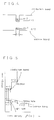
- Figure 10(a) shows a preferred embodiment of the present invention.
- the reference numeral 185 designates an n+ type GaAs substrate
- the reference numeral 186 designates an n type Al z Ga 1-z As cladding layer
- the reference numeral 187 designates an n type Al z Ga 1-z As parabola type refractive index distribution layer (z gradually changes to y)
- the reference numeral 188a designates a first Al x Ga 1-x As active layer
- the reference numeral 189 designates an Al y Ga 1-y As barrier layer
- the reference numeral 188b designates a second Al x Ga 1-x As active layer
- the reference numeral 190 designates a p type Al y Ga 1-y As parabola type refractive index distribution layer (y gradually changes to z)
- the reference numeral 191 designates a p type Al z Ga 1-z As cladding layer
- the reference numeral 192 designates a p+-
- Figure 10(b) shows an energy band structure of a semiconductor laser of the embodiment shown in Figure 10(a).
- This embodiment has a GRIN-SCH structure.
- Figure 11 shows a band structure in which double quantum well active layers 188a and 188b are arranged each side of the barrier layer 189. These active layers 188a and 188b have different thicknesses L z1 and L z2 , respectively.
- the device will be operated as follows.
- an n type electrode is produced on the side of the n+-GaAs substrate 185
- a p type stripe electrode is produced on the side of the upper p+-GaAs contact layer 192
- laser oscillator mirrors are produced vertically with the active layers 188a and 188b by such as cleavages.
- a quantum well type semiconductor laser having a plurality of quantum well active layers is produced.
- the active layers are constituted by respective quantum wells having different layer thicknesses, and a plurality of laser emissions at different wavelengths with short wavelength differences are obtained which cannot be obtained by a single quantum well active layer. Furthermore, it is possible to switch the plurality of laser emissions by a small injection current difference.
- the thicknesses of the quantum wells are varied so as to vary the energy levels of the quantum.wells.
- the reference numeral 195a designates an Al x1 Ga 1-x1 As quantum well layer
- the numeral 195b designates an Al x2 Ga 1-x2 As quantum well layer, whereas x2 > x1.
- a GRIN-SCH structure is used for the confinement of laser light, but other confinement methods can be used.
- GaAs system material is used as material, but such as InP system material can be used with the same effects as described above.
Landscapes
- Physics & Mathematics (AREA)
- Optics & Photonics (AREA)
- Condensed Matter Physics & Semiconductors (AREA)
- General Physics & Mathematics (AREA)
- Electromagnetism (AREA)
- Chemical & Material Sciences (AREA)
- Engineering & Computer Science (AREA)
- Nanotechnology (AREA)
- Life Sciences & Earth Sciences (AREA)
- Biophysics (AREA)
- Crystallography & Structural Chemistry (AREA)
- Semiconductor Lasers (AREA)
Claims (7)
- Dispositif laser à semiconducteurs, comprenant :
un ensemble de couches actives espacées (188a, 188b; 195a, 195b) empilées l'une sur l'autre;
ce dispositif laser à semiconducteurs étant caractérisé en ce que :
chacune des couches actives (188a, 188b; 195a, 195b) a une structure à un seul puits quantique ayant une épaisseur respective différente et/ou une composition respective différente, de façon que les niveaux d'énergie quantifiés de puits quantiques adjacents soient mutuellement déplacés. - Un dispositif laser selon la revendication 1, comprenant deux couches actives espacées (188a, 188b; 195a, 195b), dans lequel les niveaux d'énergie quantifiés des puits quantiques adjacents sont mutuellement déplacés de façon que le niveau d'énergie n=1 du puits quantique d'une première des couches actives (188b; 195b) se trouve à un niveau qui est situé entre les niveaux d'énergie n=1 et n=2 du puits quantique de la seconde des couches actives (188a; 195a).
- Un dispositif laser selon la revendication 2, dans lequel le niveau d'énergie n=2 du puits quantique de la seconde des couches actives (188a; 195a) se trouve à un niveau qui est situé entre les niveaux d'énergie n=1 et n=2 du puits quantique de la première des couches actives (188b; 195b).
- Un dispositif laser selon la revendication 1 ou 3, dans lequel les couches actives (188a, 188b) sont formées par un matériau ayant la même composition et elles ont des épaisseurs respectives différentes (Lz1, Lz2).
- Un dispositif laser selon les revendications 1 ou 3, dans lequel les couches actives (195a, 195b) ont les mêmes épaisseurs respectives (Lz1, Lz2) et elles sont constituées par des matériaux ayant des compositions différentes.
- Un dispositif laser selon les revendications 1 ou 3, dans lequel les couches actives ont des épaisseurs différentes et elles sont constituées par des matériaux ayant des compositions différentes.
- Utilisation d'un dispositif laser selon l'une quelconque des revendications 1 à 6, dans laquelle des oscillations à un ensemble de longueurs d'onde respectives correspondant aux niveaux d'énergie quantiques respectifs des puits quantiques, sont commutées en changeant le courant d'injection qui est injecté dans les couches actives.
Applications Claiming Priority (25)
| Application Number | Priority Date | Filing Date | Title |
|---|---|---|---|
| JP61175965A JPH0671116B2 (ja) | 1986-07-25 | 1986-07-25 | 半導体レ−ザ |
| JP175975/86 | 1986-07-25 | ||
| JP175971/86 | 1986-07-25 | ||
| JP61175971A JPS6332983A (ja) | 1986-07-25 | 1986-07-25 | 半導体レ−ザ |
| JP17597486A JPS6332986A (ja) | 1986-07-25 | 1986-07-25 | 集積化半導体レ−ザ |
| JP175967/86 | 1986-07-25 | ||
| JP175972/86 | 1986-07-25 | ||
| JP175968/86 | 1986-07-25 | ||
| JP17597286A JPS6354794A (ja) | 1986-07-25 | 1986-07-25 | 半導体レ−ザ |
| JP175966/86 | 1986-07-25 | ||
| JP17596886A JPS6332980A (ja) | 1986-07-25 | 1986-07-25 | 半導体レ−ザ |
| JP175969/86 | 1986-07-25 | ||
| JP61175970A JPS6332982A (ja) | 1986-07-25 | 1986-07-25 | 半導体レ−ザ |
| JP175973/86 | 1986-07-25 | ||
| JP61175975A JPH0634425B2 (ja) | 1986-07-25 | 1986-07-25 | 半導体レ−ザ |
| JP175970/86 | 1986-07-25 | ||
| JP175965/86 | 1986-07-25 | ||
| JP61175969A JPS6332981A (ja) | 1986-07-25 | 1986-07-25 | 半導体レ−ザアレイ |
| JP61175967A JPH0644662B2 (ja) | 1986-07-25 | 1986-07-25 | 半導体レ−ザ |
| JP17596686A JPS6332978A (ja) | 1986-07-25 | 1986-07-25 | 半導体レ−ザ |
| JP175974/86 | 1986-07-25 | ||
| JP17597386A JPS6332985A (ja) | 1986-07-25 | 1986-07-25 | 半導体レ−ザ |
| JP17628786A JPS6332989A (ja) | 1986-07-26 | 1986-07-26 | 量子井戸半導体レ−ザ |
| JP176287/86 | 1986-07-26 | ||
| EP87306520A EP0254568B1 (fr) | 1986-07-25 | 1987-07-23 | Dispositif laser à semi-conducteur |
Related Parent Applications (1)
| Application Number | Title | Priority Date | Filing Date |
|---|---|---|---|
| EP87306520.5 Division | 1987-07-23 |
Publications (3)
| Publication Number | Publication Date |
|---|---|
| EP0547043A2 EP0547043A2 (fr) | 1993-06-16 |
| EP0547043A3 EP0547043A3 (en) | 1993-08-11 |
| EP0547043B1 true EP0547043B1 (fr) | 1995-09-27 |
Family
ID=27583481
Family Applications (5)
| Application Number | Title | Priority Date | Filing Date |
|---|---|---|---|
| EP19930200587 Withdrawn EP0547042A3 (en) | 1986-07-25 | 1987-07-23 | A semiconductor laser device |
| EP87306520A Expired - Lifetime EP0254568B1 (fr) | 1986-07-25 | 1987-07-23 | Dispositif laser à semi-conducteur |
| EP93200581A Expired - Lifetime EP0547038B1 (fr) | 1986-07-25 | 1987-07-23 | Dispositif laser à semi-conducteur |
| EP93200588A Expired - Lifetime EP0547043B1 (fr) | 1986-07-25 | 1987-07-23 | Dispositif laser à semi-conducteur |
| EP93200589A Expired - Lifetime EP0547044B1 (fr) | 1986-07-25 | 1987-07-23 | Dispositif laser à semi-conducteur |
Family Applications Before (3)
| Application Number | Title | Priority Date | Filing Date |
|---|---|---|---|
| EP19930200587 Withdrawn EP0547042A3 (en) | 1986-07-25 | 1987-07-23 | A semiconductor laser device |
| EP87306520A Expired - Lifetime EP0254568B1 (fr) | 1986-07-25 | 1987-07-23 | Dispositif laser à semi-conducteur |
| EP93200581A Expired - Lifetime EP0547038B1 (fr) | 1986-07-25 | 1987-07-23 | Dispositif laser à semi-conducteur |
Family Applications After (1)
| Application Number | Title | Priority Date | Filing Date |
|---|---|---|---|
| EP93200589A Expired - Lifetime EP0547044B1 (fr) | 1986-07-25 | 1987-07-23 | Dispositif laser à semi-conducteur |
Country Status (3)
| Country | Link |
|---|---|
| US (1) | US4817110A (fr) |
| EP (5) | EP0547042A3 (fr) |
| DE (4) | DE3751548T2 (fr) |
Families Citing this family (45)
| Publication number | Priority date | Publication date | Assignee | Title |
|---|---|---|---|---|
| EP0280281B1 (fr) * | 1987-02-27 | 1994-06-15 | Canon Kabushiki Kaisha | Laser à semi-conducteur à longueur d'onde d'oscillation variable |
| JPS63258090A (ja) * | 1987-04-15 | 1988-10-25 | Sharp Corp | 半導体レ−ザ装置 |
| GB2212658B (en) * | 1987-11-13 | 1992-02-12 | Plessey Co Plc | Solid state light source |
| US4870652A (en) * | 1988-07-08 | 1989-09-26 | Xerox Corporation | Monolithic high density arrays of independently addressable semiconductor laser sources |
| US4993036A (en) * | 1988-09-28 | 1991-02-12 | Canon Kabushiki Kaisha | Semiconductor laser array including lasers with reflecting means having different wavelength selection properties |
| US5033053A (en) * | 1989-03-30 | 1991-07-16 | Canon Kabushiki Kaisha | Semiconductor laser device having plurality of layers for emitting lights of different wavelengths and method of driving the same |
| DE69009561T2 (de) * | 1989-03-31 | 1994-10-13 | Canon Kk | Halbleiterlaser zur selektiven Ausstrahlung von Licht mit verschiedenen Wellenlängen. |
| DE3934865A1 (de) * | 1989-10-19 | 1991-04-25 | Siemens Ag | Hochfrequent modulierbarer halbleiterlaser |
| DE3934998A1 (de) * | 1989-10-20 | 1991-04-25 | Standard Elektrik Lorenz Ag | Elektrisch wellenlaengenabstimmbarer halbleiterlaser |
| US5196958A (en) * | 1989-10-31 | 1993-03-23 | U.S. Philips Corporation | Optical amplifier having gain at two separated wavelengths |
| JPH03151684A (ja) * | 1989-11-08 | 1991-06-27 | Mitsubishi Electric Corp | 多波長集積化半導体レーザの製造方法 |
| US5138624A (en) * | 1989-11-16 | 1992-08-11 | The Boeing Company | Multiwavelength LED and laser diode optical source |
| FR2656168A1 (fr) * | 1989-12-15 | 1991-06-21 | Thomson Csf | Laser semiconducteur a puits quantiques modulable en intensite ou en frequence par un modulateur integre. |
| JP2808562B2 (ja) * | 1990-02-27 | 1998-10-08 | キヤノン株式会社 | 半導体光増幅素子 |
| US5124996A (en) * | 1990-03-02 | 1992-06-23 | Canon Kabushiki Kaisha | Semiconductor laser element having a plurality of layers emitting lights of different wavelengths, and its driving method |
| JPH04107976A (ja) * | 1990-08-28 | 1992-04-09 | Mitsubishi Electric Corp | 半導体レーザ装置 |
| US5224114A (en) * | 1990-11-11 | 1993-06-29 | Canon Kabushiki Kaisha | Semiconductor laser devices with a plurality of light emitting layers having different bands gaps and methods for driving the same |
| US5151915A (en) * | 1990-12-27 | 1992-09-29 | Xerox Corporation | Array and method of operating a modulated solid state laser array with reduced thermal crosstalk |
| US5126803A (en) * | 1991-03-11 | 1992-06-30 | The Boeing Company | Broadband quantum well LED |
| US5214664A (en) * | 1991-10-18 | 1993-05-25 | Xerox Corporation | Multiple wavelength semiconductor laser |
| US5200969A (en) * | 1991-10-18 | 1993-04-06 | Xerox Corporation | Switchable multiple wavelength semiconductor laser |
| EP0539015B1 (fr) * | 1991-10-18 | 1996-10-16 | Xerox Corporation | Laser à semi-conducteur à longueurs d'ondes multiples |
| JPH0696468A (ja) * | 1992-09-14 | 1994-04-08 | Canon Inc | 光記録再生装置及び半導体レーザアレイ |
| US5465263A (en) * | 1992-12-12 | 1995-11-07 | Xerox Corporation | Monolithic, multiple wavelength, dual polarization laser diode arrays |
| US5287376A (en) * | 1992-12-14 | 1994-02-15 | Xerox Corporation | Independently addressable semiconductor diode lasers with integral lowloss passive waveguides |
| DE4326522A1 (de) * | 1993-08-06 | 1995-02-09 | Siemens Ag | Programmierbares optisches Filter und optische Schaltanordnung |
| JP3303631B2 (ja) * | 1995-01-04 | 2002-07-22 | キヤノン株式会社 | 半導体量子井戸構造 |
| EP0872925B1 (fr) | 1995-09-29 | 2002-04-03 | Matsushita Electric Industrial Co., Ltd. | Laser a semi-conducteur et disque optique l'utilisant |
| FR2749447B1 (fr) * | 1996-06-04 | 1998-07-10 | France Telecom | Dispositif optique a guide de lumiere semi-conducteur, a faisceau emergent de faible divergence, application aux lasers de fabry-perot et a contre-reaction distribuee |
| US6285698B1 (en) * | 1998-09-25 | 2001-09-04 | Xerox Corporation | MOCVD growth of InGaN quantum well laser structures on a grooved lower waveguiding layer |
| US6922426B2 (en) * | 2001-12-20 | 2005-07-26 | Finisar Corporation | Vertical cavity surface emitting laser including indium in the active region |
| WO2000042685A1 (fr) * | 1999-01-11 | 2000-07-20 | The Furukawa Electric Co., Ltd. | Laser a semi-conducteur, a puits quantiques multiples, a dopage module de type n |
| US6396861B1 (en) | 1999-01-11 | 2002-05-28 | The Furukawa Electric Co., Ltd. | N-type modulation-doped multi quantum well semiconductor laser device |
| GB9912583D0 (en) | 1999-05-28 | 1999-07-28 | Arima Optoelectronics Corp | A light emitting diode having a two well system with asymmetric tunneling |
| JP2001332816A (ja) * | 2000-05-19 | 2001-11-30 | Fuji Photo Film Co Ltd | 半導体レーザ素子 |
| US6461884B1 (en) * | 2001-01-05 | 2002-10-08 | Manijeh Razeghi | Diode laser |
| GB2371405B (en) * | 2001-01-23 | 2003-10-15 | Univ Glasgow | Improvements in or relating to semiconductor lasers |
| US6834068B2 (en) * | 2001-06-29 | 2004-12-21 | Matsushita Electric Industrial Co., Ltd. | Semiconductor laser device and method for fabricating the same |
| US20030068125A1 (en) * | 2001-09-28 | 2003-04-10 | The Furukawa Electric Co., Ltd. | Semiconductor laser device, semiconductor laser module and optical fiber amplifier using the semiconductor laser module |
| GB2406968B (en) * | 2003-10-11 | 2006-12-06 | Intense Photonics Ltd | Control of output beam divergence in a semiconductor waveguide device |
| US7736370B2 (en) * | 2003-10-21 | 2010-06-15 | Zimmer Spine, Inc. | Method for interconnecting longitudinal members extending along a spinal column |
| US20050105577A1 (en) * | 2003-11-13 | 2005-05-19 | Matsushita Electric Industrial Co., Ltd. | Semiconductor laser device and manufacturing method for the same |
| US7558305B2 (en) * | 2003-12-31 | 2009-07-07 | Wisconsin Alumni Research Foundation | Intersubband mid-infrared electroluminescent semiconductor devices |
| US7403552B2 (en) * | 2006-03-10 | 2008-07-22 | Wisconsin Alumni Research Foundation | High efficiency intersubband semiconductor lasers |
| US7457338B2 (en) * | 2006-04-19 | 2008-11-25 | Wisconsin Alumni Research Foundation | Quantum well lasers with strained quantum wells and dilute nitride barriers |
Family Cites Families (18)
| Publication number | Priority date | Publication date | Assignee | Title |
|---|---|---|---|---|
| US4326176A (en) * | 1976-04-16 | 1982-04-20 | Hitachi, Ltd. | Semiconductor laser device |
| EP0014588B1 (fr) * | 1979-02-13 | 1983-12-14 | Fujitsu Limited | Dispositif semiconducteur émetteur de lumière |
| US4340967A (en) * | 1980-06-02 | 1982-07-20 | Bell Telephone Laboratories, Incorporated | Semiconductor lasers with stable higher-order modes parallel to the junction plane |
| JPS5844785A (ja) * | 1981-08-27 | 1983-03-15 | Kokusai Denshin Denwa Co Ltd <Kdd> | 半導体レ−ザ |
| JPS58140177A (ja) * | 1982-02-16 | 1983-08-19 | Kokusai Denshin Denwa Co Ltd <Kdd> | 分布帰還形半導体レ−ザ |
| JPS5929484A (ja) * | 1982-08-12 | 1984-02-16 | Fujitsu Ltd | 半導体発光装置 |
| JPH07112090B2 (ja) * | 1982-12-10 | 1995-11-29 | 富士通株式会社 | 半導体発光装置 |
| US4558449A (en) * | 1983-07-08 | 1985-12-10 | At&T Bell Laboratories | Semiconductor laser with coupled loss modulator for optical telecommunications |
| US4546480A (en) * | 1983-08-19 | 1985-10-08 | Xerox Corporation | Injection lasers with quantum size effect transparent waveguiding |
| US4589115A (en) * | 1983-09-09 | 1986-05-13 | Xerox Corporation | Wavelength tuning of quantum well heterostructure lasers using an external grating |
| US4577321A (en) * | 1983-09-19 | 1986-03-18 | Honeywell Inc. | Integrated quantum well lasers for wavelength division multiplexing |
| JPH0666509B2 (ja) * | 1983-12-14 | 1994-08-24 | 株式会社日立製作所 | 分布帰還型半導体レ−ザ装置 |
| JPS60128690A (ja) * | 1983-12-15 | 1985-07-09 | Fujitsu Ltd | 半導体発光装置 |
| US4671830A (en) * | 1984-01-03 | 1987-06-09 | Xerox Corporation | Method of controlling the modeling of the well energy band profile by interdiffusion |
| JPH0632339B2 (ja) * | 1984-12-18 | 1994-04-27 | キヤノン株式会社 | 半導体レ−ザ |
| JPS61160989A (ja) * | 1985-01-09 | 1986-07-21 | Nec Corp | 半導体レ−ザアレイ装置とその製造方法 |
| DE3581076D1 (de) * | 1985-03-14 | 1991-02-07 | Max Planck Gesellschaft | Halbleiterlaser-vorrichtungen. |
| JP2821822B2 (ja) * | 1991-04-09 | 1998-11-05 | 日本セメント 株式会社 | 軽量コンクリートの製造方法 |
-
1987
- 1987-07-23 EP EP19930200587 patent/EP0547042A3/en not_active Withdrawn
- 1987-07-23 EP EP87306520A patent/EP0254568B1/fr not_active Expired - Lifetime
- 1987-07-23 EP EP93200581A patent/EP0547038B1/fr not_active Expired - Lifetime
- 1987-07-23 EP EP93200588A patent/EP0547043B1/fr not_active Expired - Lifetime
- 1987-07-23 DE DE3751548T patent/DE3751548T2/de not_active Expired - Fee Related
- 1987-07-23 DE DE3751535T patent/DE3751535T2/de not_active Expired - Fee Related
- 1987-07-23 DE DE87306520T patent/DE3787769T2/de not_active Expired - Fee Related
- 1987-07-23 DE DE3751549T patent/DE3751549T2/de not_active Expired - Fee Related
- 1987-07-23 EP EP93200589A patent/EP0547044B1/fr not_active Expired - Lifetime
- 1987-07-24 US US07/078,393 patent/US4817110A/en not_active Expired - Lifetime
Also Published As
| Publication number | Publication date |
|---|---|
| DE3787769T2 (de) | 1994-02-24 |
| EP0547042A2 (fr) | 1993-06-16 |
| EP0547044A3 (en) | 1993-08-11 |
| EP0547044A2 (fr) | 1993-06-16 |
| EP0547042A3 (en) | 1993-08-18 |
| DE3751549D1 (de) | 1995-11-02 |
| EP0547043A3 (en) | 1993-08-11 |
| DE3751535T2 (de) | 1996-02-22 |
| EP0547038B1 (fr) | 1995-09-20 |
| DE3751548T2 (de) | 1996-04-11 |
| DE3751535D1 (de) | 1995-10-26 |
| EP0254568B1 (fr) | 1993-10-13 |
| DE3751549T2 (de) | 1996-03-21 |
| EP0254568A2 (fr) | 1988-01-27 |
| EP0547038A3 (en) | 1993-08-18 |
| EP0547044B1 (fr) | 1995-09-27 |
| US4817110A (en) | 1989-03-28 |
| DE3751548D1 (de) | 1995-11-02 |
| EP0547043A2 (fr) | 1993-06-16 |
| EP0254568A3 (en) | 1988-07-20 |
| EP0547038A2 (fr) | 1993-06-16 |
| DE3787769D1 (de) | 1993-11-18 |
Similar Documents
| Publication | Publication Date | Title |
|---|---|---|
| EP0547043B1 (fr) | Dispositif laser à semi-conducteur | |
| US5214664A (en) | Multiple wavelength semiconductor laser | |
| EP0390167B1 (fr) | Laser à semi-conducteur muni de couches multiples pour l'émission de lumière de longueurs d'ondes différentes et méthode de commande | |
| US5982799A (en) | Multiple-wavelength laser diode array using quantum well band filling | |
| US5200969A (en) | Switchable multiple wavelength semiconductor laser | |
| US4815087A (en) | High speed stable light emitting semiconductor device with low threshold current | |
| US6026110A (en) | Distributed feedback semiconductor laser with gain modulation | |
| JPH07202327A (ja) | 光半導体素子 | |
| US4982408A (en) | Variable oscillation wavelength semiconduction laser device | |
| US5073805A (en) | Semiconductor light emitting device including a hole barrier contiguous to an active layer | |
| US6925103B2 (en) | Gain-coupled DFB laser diode | |
| JPS59119783A (ja) | 半導体発光装置 | |
| JPS6332982A (ja) | 半導体レ−ザ | |
| JPH03151684A (ja) | 多波長集積化半導体レーザの製造方法 | |
| JPH04245493A (ja) | 多波長半導体レーザ素子及びその駆動方法 | |
| US20030094617A1 (en) | Laser diode | |
| EP0539015B1 (fr) | Laser à semi-conducteur à longueurs d'ondes multiples | |
| JP3875799B2 (ja) | 半導体レーザ装置 | |
| JP3149962B2 (ja) | 多波長半導体レーザ素子及びその駆動方法 | |
| JP2526898B2 (ja) | 半導体レ−ザおよびその使用方法 | |
| JPH0821758B2 (ja) | 半導体レ−ザおよびその使用方法 | |
| JP2703618B2 (ja) | 半導体レーザ装置 | |
| JP2683092B2 (ja) | 半導体レーザ素子 | |
| JPH0634425B2 (ja) | 半導体レ−ザ | |
| JPS6332979A (ja) | 半導体レ−ザ |
Legal Events
| Date | Code | Title | Description |
|---|---|---|---|
| PUAI | Public reference made under article 153(3) epc to a published international application that has entered the european phase |
Free format text: ORIGINAL CODE: 0009012 |
|
| AC | Divisional application: reference to earlier application |
Ref document number: 254568 Country of ref document: EP |
|
| AK | Designated contracting states |
Kind code of ref document: A2 Designated state(s): DE FR GB |
|
| PUAL | Search report despatched |
Free format text: ORIGINAL CODE: 0009013 |
|
| AK | Designated contracting states |
Kind code of ref document: A3 Designated state(s): DE FR GB |
|
| 17P | Request for examination filed |
Effective date: 19931102 |
|
| 17Q | First examination report despatched |
Effective date: 19940330 |
|
| GRAA | (expected) grant |
Free format text: ORIGINAL CODE: 0009210 |
|
| AC | Divisional application: reference to earlier application |
Ref document number: 254568 Country of ref document: EP |
|
| AK | Designated contracting states |
Kind code of ref document: B1 Designated state(s): DE FR GB |
|
| REF | Corresponds to: |
Ref document number: 3751548 Country of ref document: DE Date of ref document: 19951102 |
|
| ET | Fr: translation filed | ||
| REG | Reference to a national code |
Ref country code: GB Ref legal event code: 746 Effective date: 19960611 |
|
| PLBE | No opposition filed within time limit |
Free format text: ORIGINAL CODE: 0009261 |
|
| STAA | Information on the status of an ep patent application or granted ep patent |
Free format text: STATUS: NO OPPOSITION FILED WITHIN TIME LIMIT |
|
| 26N | No opposition filed | ||
| REG | Reference to a national code |
Ref country code: FR Ref legal event code: D6 |
|
| REG | Reference to a national code |
Ref country code: GB Ref legal event code: IF02 |
|
| PGFP | Annual fee paid to national office [announced via postgrant information from national office to epo] |
Ref country code: FR Payment date: 20020709 Year of fee payment: 16 |
|
| PGFP | Annual fee paid to national office [announced via postgrant information from national office to epo] |
Ref country code: GB Payment date: 20020717 Year of fee payment: 16 |
|
| PGFP | Annual fee paid to national office [announced via postgrant information from national office to epo] |
Ref country code: DE Payment date: 20020731 Year of fee payment: 16 |
|
| PG25 | Lapsed in a contracting state [announced via postgrant information from national office to epo] |
Ref country code: GB Free format text: LAPSE BECAUSE OF NON-PAYMENT OF DUE FEES Effective date: 20030723 |
|
| PG25 | Lapsed in a contracting state [announced via postgrant information from national office to epo] |
Ref country code: DE Free format text: LAPSE BECAUSE OF NON-PAYMENT OF DUE FEES Effective date: 20040203 |
|
| GBPC | Gb: european patent ceased through non-payment of renewal fee |
Effective date: 20030723 |
|
| PG25 | Lapsed in a contracting state [announced via postgrant information from national office to epo] |
Ref country code: FR Free format text: LAPSE BECAUSE OF NON-PAYMENT OF DUE FEES Effective date: 20040331 |
|
| REG | Reference to a national code |
Ref country code: FR Ref legal event code: ST |