EP0550088A2 - Bildverarbeitungsanordnung - Google Patents
Bildverarbeitungsanordnung Download PDFInfo
- Publication number
- EP0550088A2 EP0550088A2 EP92203886A EP92203886A EP0550088A2 EP 0550088 A2 EP0550088 A2 EP 0550088A2 EP 92203886 A EP92203886 A EP 92203886A EP 92203886 A EP92203886 A EP 92203886A EP 0550088 A2 EP0550088 A2 EP 0550088A2
- Authority
- EP
- European Patent Office
- Prior art keywords
- image
- pixel
- pixel values
- input
- row
- Prior art date
- Legal status (The legal status is an assumption and is not a legal conclusion. Google has not performed a legal analysis and makes no representation as to the accuracy of the status listed.)
- Granted
Links
Images


Classifications
-
- H—ELECTRICITY
- H04—ELECTRIC COMMUNICATION TECHNIQUE
- H04N—PICTORIAL COMMUNICATION, e.g. TELEVISION
- H04N5/00—Details of television systems
- H04N5/44—Receiver circuitry for the reception of television signals according to analogue transmission standards
-
- G—PHYSICS
- G06—COMPUTING OR CALCULATING; COUNTING
- G06T—IMAGE DATA PROCESSING OR GENERATION, IN GENERAL
- G06T3/00—Geometric image transformations in the plane of the image
- G06T3/40—Scaling of whole images or parts thereof, e.g. expanding or contracting
- G06T3/4007—Scaling of whole images or parts thereof, e.g. expanding or contracting based on interpolation, e.g. bilinear interpolation
Definitions
- the invention relates to an image processing apparatus comprising image memory means for the storage of an input array of pixel values defining an input image and a microprocessor operating under control of a program stored in a program memory to systematically select pixel values of the input array to generate successive output pixel values defining an output image, the system of selection being dependent on at least one parameter value received by the arrangement.
- Image processing is ideally performed by specialised hardware, but there is an increasing demand for image processing to be performed by general purpose microprocessors in personal computers and home entertainment systems.
- processors are not optimised for the operations required, and tend to take many seconds or even minutes to process a single image.
- One reason for this is the need for pixel-by-pixel decisions as to which input pixel values should be selected to generate each output pixel value and what weighting coefficients to apply.
- Another reason for this is the time taken to multiply input pixel values by the necessary weighting coefficients.
- digitised images are now being published on media including on-line data bases and optical memory discs (CD-ROM).
- CD-ROM optical memory discs
- the user can selectively zoom in or out on (enlarge or reduce) a selected area of the stored image.
- zooming requires filtering of pixel data, for example by interpolation, in order to avoid obtrusive mosaic effects and aliasing.
- the Photo CD system described at pages 316-323 in IEEE ICCE Digest 1991, even enables photographs taken by the individual consumer to be digitised and stored on CD-ROM for selective retrieval and display.
- the Photo CD player itself comprises essentially dedicated hardware for display of the images with very limited capabilities for panning and zooming different parts of an image.
- CD-I Compact Disc Interactive
- the fact that the CD-I player includes a general purpose microprocessor controllable by programs which themselves are stored on the disc means that in principle any zoom and filter function can be applied to the retrieved data before display.
- a problem that arises in practice is the time taken by the microprocessor to perform a generalised zoom and filtering operation with a user defined scaling factor.
- the same problem arises in the retrieval and display of images using general purpose personal computers, for example in so-called desktop publishing.
- the invention provides an image processing arrangement as set forth in the opening paragraph, characterised in that the programmed microprocessor forms
- Each subset of output pixel values may typically comprise one pixel row of the output image.
- the per-pixel decision overhead can be reduced by a factor of 512.
- Figures present an embodiment in the form of an interactive multimedia application using the Compact Disc Interactive (CD-I) player to process images stored on optical disc.
- CD-I Compact Disc Interactive
- the Compact Disc-Interactive (CD-I) player comprises a compact disc player module CDP to which is connected a compact disc digital audio controller decoder CDDA and a compact disc control unit CDCU.
- the decoder CDDA is connected to an audio processing unit APU which feeds two loudspeakers LSL and LSR.
- the CD control unit CDCU is connected to a system bus SB along which various digital signals are passed.
- Also connected to the system bus SB are a microprocessor unit MPU, a DMA controller DMA, a non-volatile random access memory NVRAM, a clock calendar unit C/C, a read-only memory containing the real-time operating system CDRTOS, a keyboard KB, a pointing device INP, and an access controller AC.
- the access controller controls the reading from and writing to a random access memory RAM which is split into two banks zero and one.
- the access controller is also connected to a video decoder VD which in turn feeds a video generator VRGB, the output of which is connected to a video display unit VDU.
- a video decoder VD which in turn feeds a video generator VRGB, the output of which is connected to a video display unit VDU.
- an adaptive pulse code modulation decoder ADPCM which feeds the audio processing unit APU.
- the video decoder VD in the CD-I player can read picture information which has been transferred from a compact disc (CD-ROM) to the random access memory RAM, which leads to the generation of appropriate video signals for the VDU by the video generator VRGB.
- CD-ROM compact disc
- the Philips/Kluwer book describes how various picture coding formats are available.
- DYUV 'Delta-YUV'
- DCT Discrete Cosine Transform
- the program can be stored for example in a separate CD-I section of a Photo CD disc, in a manner transparent to the user. Even if the user does not require variable zoom and rotation facilities, the CD-I player itself may require to perform some horizontal or vertical expansion to correct for the difference between the aspect ratio of the stored pixels (square) and that of the displayed pixels (rectangular).
- Figure 2 illustrates a zoom and filter operation for a small representative array of pixels.
- the input image is defined by rows 0 to 4 of input pixel values numbered 0 to 6 in each row and positioned on a square grid.
- the input pixel positions are represented by circles "o" at integer pixel positions (0,0), (0,1) and so forth.
- An input pixel value is received for each circled position and each row of pixel values is stored in memory at a series of locations following a row start address.
- the rows may be stored sequentially, but this is not necessary as they can be addressed via a row table giving the start address of each successive row of the image.
- each pixel value occupies one byte (8-bit value) and represents only one component of the pixel colour.
- luminance (Y) and chrominance (U and V) bytes are stored on the CD-ROM, but with four times as many Y as U or V.
- Y luminance
- U and V chrominance
- the skilled reader will appreciate that other component systems, notably RGB, can be used, and that the three components can in such systems be treated independently (taking due account of gamma correction and other non-linearities).
- the description presented here will concern the processing of one component value only, with any other components being processed in like manner.
- Figure 3 shows how the bilinear interpolation of four input values to yield each output value can be reduced to two separate linear interpolations in the vertical and then the horizontal directions.
- rows of intermediate pixel values "+" are generated from pairs of input pixel values in adjacent lines by linear interpolation. For example an intermediate value corresponding to position (1.6, 1.0) is interpolated from the input values for positions (1,1) and (2,1), and another intermediate value is generated for position (1.6, 2.0) by interpolation between the input values for positions (1,2) and (2,2). It may be noted that the only decision overhead per pixel in such an operation is to check for the end of the rows, since the fractional coefficients (0.6 and 0.4 for this row) are constant across the row, and every intermediate position "+" is at an integer position on the input pixel grid.
- Step (c) in its turn includes a number of operations to select a fractional coefficient by which to multiply each input value. Even if the microprocessor has dedicated multiplier hardware, these selection operations can be very time-consuming.
- Listing 1 presented as an appendix at the end of this description, is a 'C' language source code listing of a program to be run by the microprocessor MPU of the CD-I player to compile quickly a machine code program segment which when executed will generate one row of output pixels, scaled with linear interpolation from a row of input pixel values.
- a short example program segment generated for a particular set of parameter values is presented in Listing 2. From the following description, the skilled reader will appreciate that decisions are taken by the compiler of Listing 1 once only, so that the machine code row filter of Listing 2, although occupying more program memory than a conventional filter program, can generate row upon row of filtered pixel values without further decision overhead.
- the listings will be largely self-explanatory to the skilled reader familiar with the 'C' language, and with assembly language for the 68000 series of microprocessors, as used in the CD-I player. Of course equivalent code can be constructed for other microprocessors.
- the first section (A) of the compiler program (Listing 1) defines certain constants which are at least parts of specific instructions for the target microprocessor.
- a constant LOADTOD0 is a 16-bit value 1018 (Hexadecimal). To the 68000 series microprocessor MPU, this is an instruction "move.b (a0)+,d0" for causing a single byte, found in a memory location specified by an address stored in internal address register a0, to be copied into internal data register d0, with a post-increment of the address in a0.
- this instruction can be used in the compiled row filter program to load an input pixel value from the memory, while updating the address in register a0 to point to the next input pixel value in the row.
- Constant LOADTOD1 1218 causes the pixel value to be loaded to register D1 (move.b (a0)+,d1).
- constant STOREFROMD0 is a 16-bit value 12CO (hexadecimal).
- this is the instruction "move.b dO,(a1)+” causing a single byte found in the internal data register dO to be copied to a memory location specified by the address stored in internal address register a1, with an automatic post-increment of that stored address.
- this instruction can be used in the compiled program segment to write an output pixel value and increment the address in register a1 ready for storage of the next output pixel value.
- STOREFROMD1 and STOREFROMD2 perform the same function where the output pixel value to be stored is found in register d1 or d2 respectively.
- each base address a2 to a6 refers to a pair of tables 0.1/0.9, 0.2/0.8, 0.3/0.7, 0.4/0.6, 0.5/0.5.
- the 0.1 table for example, stores for each expected 8-bit pixel value an 8-bit value for 0.1 times that pixel value.
- the 0.1 table begins at location (a2) minus an offset of 120, while the 0.9 table begins at location (a2) plus an offset of 120.
- the pairs of tables are complementary even to the extent that the two tables for coefficient 0.5 are not identical: any rounding error in the first table entry is compensated in the second table entry.
- register d2 is used to accumulate weighted pixel values.
- the first words of the requisite machine code instructions are defined in parts C and D in the Listing 1. This first word must select the look-up table (by selecting a register a2 to a6), and nine different opcodes are required depending on whether a required fractional coefficient is 0.1, 0.2 and so on up to 0.9. Note that the third and seventh codes are the same (1434 hex), because the required look up table base address is in register a4 whether the fractional coefficient is 0.3 or 0.7.
- the codes at C in Listing 1 specify a byte is to be loaded (move.b) to register d2, from an effective address to be specified in the mode "address register indirect with index and displacement".
- the codes at D in Listing 1 specify a byte is to be added (add.b) to the contents of register d2, with similar addressing.
- a look-up table with 64 entries is defined for use in quantising a fractional value represented in 64ths to one represented in tenths.
- variables “samplein0” and “samplein1” identify the input pixel value in register d0 and d1 respectively, “inputposn” holds the position along the line of input values with an 16-bit fractional component; “output” is the output pixel value; “fractional” is the fractional part of “inputposn” truncated to 6 bits; “intposn” is the integer part of “inputposn”; “quantfrac” is “fraction” quantised by tenths (0.1, 0.2, 0.3 etc.); “basereg” indicates whether register d0 or d1 holds the left most input pixel value; “secondreg” indicates whether register d0 to d1 holds the following input pixel value; “regused0” and “regused1” are flags to indicate whether the register d0 or d1 is in use.
- At G begins a "for" loop, to be executed once for every output pixel value from 0 to "outputsize”.
- the variables listed above are initialised.
- At I it is checked whether the quantisation to tenths has pushed the sample position to the next input value.
- the two sample values required for interpolation correspond to input pixel positions "intposn” and "intposn” plus one.
- At J it is determined whether the first required sample value is already in a register d0 or d1, and the flags are set accordingly.
- At K it is determined whether the second value is already present.
- the compiler proceeds at N to store a machine code command "move.b d0,(a1)+". After only two instructions in the compiled filter of Listing 2, the first output pixel value will have been stored.
- the first instruction is "move.b" instruction which uses the quantised function to address a value in the appropriate look-up table and store it in register d2.
- address register a3 is used to address the 0.2/0.8 table
- 0.2 times the first input pixel value is loaded from the look-up table into register D2.
- the next instruction is an "add.b” instruction, such that (in line 5 of Listing 2) 0.8 times the second input pixel value is added to register d2.
- the instruction "move.b d2,(a1)+” is written to provide for storage of the interpolated output pixel alone.
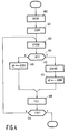
- Figure 4 shows in flowchart form a routine for achieving the uniform scaling by a variable factor using the compiled filter.
- the flow chart will be broadly similar for any process implemented with a compiled processing function according to the invention, with only the detail changing within the individual steps.
- At 400 information is received of the locations of rows of input pixel values.
- the apparatus receives from the user the desired scaling factors, cropping information and so forth.
- a filter subroutine is compiled and the filtering can begin.
- a current vertical position is determined, taking into account the cropping information and the vertical scaling factor.
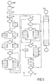
- Figure 5 shows schematic flowcharts COMP and FILT corresponding to the compiling routine of step 402 (Listing 1) and the compiled row filter routine 408 (Listing 2).
- the individual steps of the routines are not identified in the flowchart for reasons of space but the step reference letters A to R of Listing 1 are included in the flowchart COMP, to aid the comparison.
- the flowchart uses the normal convention to distinguish between simple actions, shown as rectangular boxes, and decision points, shown as diamond (rhomboid) boxes.
- the steps H-R and the test at G'' are executed once for every output pixel value to be generated by the compiled row filter routine FILT.
- the compiling process COMP therefore includes no less than ten decision points (conditional branches) for every pixel of the row.
- the flowchart FILT shows that the compiled row filter of Listing 2 includes only a linear sequence of simple actions, with no decision points.
- step 401 (COMP) is performed only once for the image
- step 408 (FILT) is performed for every row of the image to be filtered, with a decision 414 per row to detect the last row of the image.
- the number of decisions involved is therefore ten times the number of pixels in a row plus one times the number of rows.
- this formula gives an "overhead" of 4096 decisions in addition to the actions necessary to generate the output image pixel values.
- a conventional generic filter routine would perform a process corresponding effectively to the step 401 (COMP) for every row of the image, as illustrated by step 414' in broken lines in Figure 5. This would then involve performing the same ten decisions (loop H to G") for every single pixel of the image.
- To implement a variable filter using a conventional software method would thus involve an overhead of nearly a million decisions for the same size of image. With any typical microprocessor this overhead will add significantly to the time taken to filter the image.
- the decision overhead required in the novel filter implementation of Figure 4 is comparatively negligible, and leads to a much faster filtering of images.
- the decision overhead by the conventional method will quadruple, while that by the novel method will only double.
- the invention is of course not limited to zoom and filter operations, nor is the filtering limited to linear interpolation. Rotations may also be effected, either directly or as a succession of two shear operations, as is known in the art.
- the skilled reader will appreciate that the current pixel position ("inputposition" in Listing 1) will vary in two dimensions, not just along a row. Many other variations will be apparent, for example in the number of input samples being combined (kernel size), the use of hardware multipliers instead of look-up tables and so forth.
- the compiled filter program segment will occupy some kilobytes of program memory while in use.
Landscapes
- Engineering & Computer Science (AREA)
- Physics & Mathematics (AREA)
- General Physics & Mathematics (AREA)
- Theoretical Computer Science (AREA)
- Multimedia (AREA)
- Signal Processing (AREA)
- Image Processing (AREA)
- Apparatus For Radiation Diagnosis (AREA)
- Ultra Sonic Daignosis Equipment (AREA)
- Display Devices Of Pinball Game Machines (AREA)
- Automatic Focus Adjustment (AREA)
- Digital Computer Display Output (AREA)
- Controls And Circuits For Display Device (AREA)
- Processing Or Creating Images (AREA)
- Studio Circuits (AREA)
Applications Claiming Priority (2)
| Application Number | Priority Date | Filing Date | Title |
|---|---|---|---|
| GB9127108 | 1991-12-20 | ||
| GB919127108A GB9127108D0 (en) | 1991-12-20 | 1991-12-20 | Image processing arrangements |
Publications (3)
| Publication Number | Publication Date |
|---|---|
| EP0550088A2 true EP0550088A2 (de) | 1993-07-07 |
| EP0550088A3 EP0550088A3 (de) | 1994-03-23 |
| EP0550088B1 EP0550088B1 (de) | 1998-05-20 |
Family
ID=10706625
Family Applications (1)
| Application Number | Title | Priority Date | Filing Date |
|---|---|---|---|
| EP92203886A Expired - Lifetime EP0550088B1 (de) | 1991-12-20 | 1992-12-14 | Bildverarbeitungsanordnung |
Country Status (12)
| Country | Link |
|---|---|
| EP (1) | EP0550088B1 (de) |
| JP (1) | JPH05274425A (de) |
| KR (1) | KR930015767A (de) |
| CN (1) | CN1073791A (de) |
| AT (1) | ATE166473T1 (de) |
| AU (1) | AU662029B2 (de) |
| BR (1) | BR9205047A (de) |
| CA (1) | CA2085712A1 (de) |
| DE (1) | DE69225572T2 (de) |
| GB (1) | GB9127108D0 (de) |
| MX (1) | MX9207107A (de) |
| SG (1) | SG44030A1 (de) |
Cited By (1)
| Publication number | Priority date | Publication date | Assignee | Title |
|---|---|---|---|---|
| EP0683472A3 (de) * | 1994-05-20 | 1996-04-03 | Ibm | Geometrische Transformation von Bilderdaten. |
Families Citing this family (3)
| Publication number | Priority date | Publication date | Assignee | Title |
|---|---|---|---|---|
| DE69842250D1 (de) | 1997-06-24 | 2011-06-16 | Sharp Kk | Optisches Wiedergabegerät und optisches Speichersystem mit diesem Gerät und einem Medium |
| JP4926886B2 (ja) * | 2007-08-24 | 2012-05-09 | 富士フイルム株式会社 | 画像処理装置、画像処理プログラム |
| CN106175839A (zh) * | 2015-04-30 | 2016-12-07 | 烟台鑫丰源电站设备有限公司 | 用于超声相控阵的扇形扫描成像的扫描检测方法和装置 |
Family Cites Families (3)
| Publication number | Priority date | Publication date | Assignee | Title |
|---|---|---|---|---|
| EP0232081B1 (de) * | 1986-01-22 | 1994-03-30 | Konica Corporation | Bildverarbeitungssystem mit Fähigkeit zum Vergrössungs- und Reduzier-Betrieb |
| EP0312235A3 (de) * | 1987-10-13 | 1991-09-11 | AT&T Corp. | Graphischer Bildeditor |
| JP2722123B2 (ja) * | 1989-12-08 | 1998-03-04 | パイオニア株式会社 | 車載ナビゲーション装置 |
-
1991
- 1991-12-14 SG SG1996009516A patent/SG44030A1/en unknown
- 1991-12-20 GB GB919127108A patent/GB9127108D0/en active Pending
-
1992
- 1992-12-09 MX MX9207107A patent/MX9207107A/es not_active IP Right Cessation
- 1992-12-14 EP EP92203886A patent/EP0550088B1/de not_active Expired - Lifetime
- 1992-12-14 DE DE69225572T patent/DE69225572T2/de not_active Expired - Fee Related
- 1992-12-14 AT AT92203886T patent/ATE166473T1/de active
- 1992-12-16 AU AU30197/92A patent/AU662029B2/en not_active Ceased
- 1992-12-17 BR BR9205047A patent/BR9205047A/pt not_active Application Discontinuation
- 1992-12-17 CA CA002085712A patent/CA2085712A1/en not_active Abandoned
- 1992-12-17 CN CN92114468A patent/CN1073791A/zh active Pending
- 1992-12-17 KR KR1019920024551A patent/KR930015767A/ko not_active Ceased
- 1992-12-21 JP JP4340572A patent/JPH05274425A/ja active Pending
Cited By (2)
| Publication number | Priority date | Publication date | Assignee | Title |
|---|---|---|---|---|
| EP0683472A3 (de) * | 1994-05-20 | 1996-04-03 | Ibm | Geometrische Transformation von Bilderdaten. |
| US5838297A (en) * | 1994-05-20 | 1998-11-17 | International Business Machines Corporation | Method for color image scaling and other geometrical transformations |
Also Published As
| Publication number | Publication date |
|---|---|
| JPH05274425A (ja) | 1993-10-22 |
| ATE166473T1 (de) | 1998-06-15 |
| SG44030A1 (en) | 1997-11-14 |
| KR930015767A (ko) | 1993-07-24 |
| CA2085712A1 (en) | 1993-06-21 |
| GB9127108D0 (en) | 1992-02-19 |
| AU3019792A (en) | 1993-06-24 |
| DE69225572T2 (de) | 1998-11-26 |
| EP0550088A3 (de) | 1994-03-23 |
| DE69225572D1 (de) | 1998-06-25 |
| AU662029B2 (en) | 1995-08-17 |
| CN1073791A (zh) | 1993-06-30 |
| EP0550088B1 (de) | 1998-05-20 |
| BR9205047A (pt) | 1993-06-22 |
| MX9207107A (es) | 1993-07-01 |
Similar Documents
| Publication | Publication Date | Title |
|---|---|---|
| US7155601B2 (en) | Multi-element operand sub-portion shuffle instruction execution | |
| US6041404A (en) | Dual function system and method for shuffling packed data elements | |
| US5923316A (en) | Optimized color space conversion | |
| EP0013069B1 (de) | Datenverarbeitungsgerät und Verfahren zur Verarbeitung von Video-Information | |
| CA2190797C (en) | High speed digital video decompression | |
| US6211892B1 (en) | System and method for performing an intra-add operation | |
| US5625374A (en) | Method for parallel interpolation of images | |
| US5369418A (en) | Display apparatus, a method of storing an image and a storage device wherein an image has been stored | |
| TWI251787B (en) | Apparatus, method and system for filtering two-dimensional (2-D) data | |
| Harney et al. | The i750 video processor: A total multimedia solution | |
| EP0551990A1 (de) | Verfahren und Vorrichtung zur Kompression von digitalen Videosignalen | |
| EP0550088B1 (de) | Bildverarbeitungsanordnung | |
| JPS6049332B2 (ja) | マイクロプログラム制御方式 | |
| JP2776489B2 (ja) | ビデオ画像のシーケンス内の変化の位置を符号化する方法 | |
| JP3106060B2 (ja) | 信号プロセッサ | |
| CN1497592A (zh) | 存储受控单元的控制命令的存储媒体 | |
| US5977986A (en) | Image encoding for faster decoding | |
| US6774952B1 (en) | Bandwidth management | |
| EP0404397B1 (de) | Bildverarbeitungssystem | |
| JPH0778084A (ja) | マルチメディアシステム | |
| US6307553B1 (en) | System and method for performing a MOVHPS-MOVLPS instruction | |
| US6741294B2 (en) | Digital signal processor and digital signal processing method | |
| US5426514A (en) | Method of gray scaling facsimile images | |
| JP3163975B2 (ja) | 符号化プロセッサ | |
| JPH05219468A (ja) | 静止画固体記憶装置 |
Legal Events
| Date | Code | Title | Description |
|---|---|---|---|
| PUAI | Public reference made under article 153(3) epc to a published international application that has entered the european phase |
Free format text: ORIGINAL CODE: 0009012 |
|
| AK | Designated contracting states |
Kind code of ref document: A2 Designated state(s): AT BE CH DE DK ES FR GB IT LI NL SE |
|
| PUAL | Search report despatched |
Free format text: ORIGINAL CODE: 0009013 |
|
| AK | Designated contracting states |
Kind code of ref document: A3 Designated state(s): AT BE CH DE DK ES FR GB IT LI NL SE |
|
| 17P | Request for examination filed |
Effective date: 19940908 |
|
| 17Q | First examination report despatched |
Effective date: 19960723 |
|
| GRAG | Despatch of communication of intention to grant |
Free format text: ORIGINAL CODE: EPIDOS AGRA |
|
| RHK1 | Main classification (correction) |
Ipc: G06T 3/00 |
|
| GRAG | Despatch of communication of intention to grant |
Free format text: ORIGINAL CODE: EPIDOS AGRA |
|
| GRAH | Despatch of communication of intention to grant a patent |
Free format text: ORIGINAL CODE: EPIDOS IGRA |
|
| GRAH | Despatch of communication of intention to grant a patent |
Free format text: ORIGINAL CODE: EPIDOS IGRA |
|
| GRAA | (expected) grant |
Free format text: ORIGINAL CODE: 0009210 |
|
| AK | Designated contracting states |
Kind code of ref document: B1 Designated state(s): AT BE CH DE DK ES FR GB IT LI NL SE |
|
| PG25 | Lapsed in a contracting state [announced via postgrant information from national office to epo] |
Ref country code: IT Free format text: LAPSE BECAUSE OF FAILURE TO SUBMIT A TRANSLATION OF THE DESCRIPTION OR TO PAY THE FEE WITHIN THE PRE;WARNING: LAPSES OF ITALIAN PATENTS WITH EFFECTIVE DATE BEFORE 2007 MAY HAVE OCCURRED AT ANY TIME BEFORE 2007. THE CORRECT EFFECTIVE DATE MAY BE DIFFERENT FROM THE ONE RECORDED.SCRIBED TIME-LIMIT Effective date: 19980520 Ref country code: NL Free format text: LAPSE BECAUSE OF FAILURE TO SUBMIT A TRANSLATION OF THE DESCRIPTION OR TO PAY THE FEE WITHIN THE PRESCRIBED TIME-LIMIT Effective date: 19980520 Ref country code: CH Free format text: LAPSE BECAUSE OF FAILURE TO SUBMIT A TRANSLATION OF THE DESCRIPTION OR TO PAY THE FEE WITHIN THE PRESCRIBED TIME-LIMIT Effective date: 19980520 Ref country code: BE Free format text: LAPSE BECAUSE OF FAILURE TO SUBMIT A TRANSLATION OF THE DESCRIPTION OR TO PAY THE FEE WITHIN THE PRESCRIBED TIME-LIMIT Effective date: 19980520 Ref country code: AT Free format text: LAPSE BECAUSE OF FAILURE TO SUBMIT A TRANSLATION OF THE DESCRIPTION OR TO PAY THE FEE WITHIN THE PRESCRIBED TIME-LIMIT Effective date: 19980520 Ref country code: ES Free format text: THE PATENT HAS BEEN ANNULLED BY A DECISION OF A NATIONAL AUTHORITY Effective date: 19980520 Ref country code: LI Free format text: LAPSE BECAUSE OF FAILURE TO SUBMIT A TRANSLATION OF THE DESCRIPTION OR TO PAY THE FEE WITHIN THE PRESCRIBED TIME-LIMIT Effective date: 19980520 |
|
| REF | Corresponds to: |
Ref document number: 166473 Country of ref document: AT Date of ref document: 19980615 Kind code of ref document: T |
|
| REG | Reference to a national code |
Ref country code: CH Ref legal event code: EP |
|
| REF | Corresponds to: |
Ref document number: 69225572 Country of ref document: DE Date of ref document: 19980625 |
|
| ET | Fr: translation filed | ||
| PG25 | Lapsed in a contracting state [announced via postgrant information from national office to epo] |
Ref country code: SE Free format text: LAPSE BECAUSE OF FAILURE TO SUBMIT A TRANSLATION OF THE DESCRIPTION OR TO PAY THE FEE WITHIN THE PRESCRIBED TIME-LIMIT Effective date: 19980820 Ref country code: DK Free format text: LAPSE BECAUSE OF FAILURE TO SUBMIT A TRANSLATION OF THE DESCRIPTION OR TO PAY THE FEE WITHIN THE PRESCRIBED TIME-LIMIT Effective date: 19980820 |
|
| RAP4 | Party data changed (patent owner data changed or rights of a patent transferred) |
Owner name: PHILIPS ELECTRONICS UK LIMITED Owner name: KONINKLIJKE PHILIPS ELECTRONICS N.V. |
|
| REG | Reference to a national code |
Ref country code: FR Ref legal event code: CD |
|
| NLV1 | Nl: lapsed or annulled due to failure to fulfill the requirements of art. 29p and 29m of the patents act | ||
| REG | Reference to a national code |
Ref country code: CH Ref legal event code: PL |
|
| PG25 | Lapsed in a contracting state [announced via postgrant information from national office to epo] |
Ref country code: GB Free format text: LAPSE BECAUSE OF NON-PAYMENT OF DUE FEES Effective date: 19981214 |
|
| PLBE | No opposition filed within time limit |
Free format text: ORIGINAL CODE: 0009261 |
|
| 26N | No opposition filed | ||
| GBPC | Gb: european patent ceased through non-payment of renewal fee |
Effective date: 19981214 |
|
| PG25 | Lapsed in a contracting state [announced via postgrant information from national office to epo] |
Ref country code: FR Free format text: LAPSE BECAUSE OF NON-PAYMENT OF DUE FEES Effective date: 19990831 |
|
| REG | Reference to a national code |
Ref country code: FR Ref legal event code: ST |
|
| PG25 | Lapsed in a contracting state [announced via postgrant information from national office to epo] |
Ref country code: DE Free format text: LAPSE BECAUSE OF NON-PAYMENT OF DUE FEES Effective date: 19991001 |