EP0550880A2 - Dispositif de formation d'images - Google Patents
Dispositif de formation d'images Download PDFInfo
- Publication number
- EP0550880A2 EP0550880A2 EP92121856A EP92121856A EP0550880A2 EP 0550880 A2 EP0550880 A2 EP 0550880A2 EP 92121856 A EP92121856 A EP 92121856A EP 92121856 A EP92121856 A EP 92121856A EP 0550880 A2 EP0550880 A2 EP 0550880A2
- Authority
- EP
- European Patent Office
- Prior art keywords
- toner
- control grid
- image
- electrodes
- transfer belt
- Prior art date
- Legal status (The legal status is an assumption and is not a legal conclusion. Google has not performed a legal analysis and makes no representation as to the accuracy of the status listed.)
- Granted
Links
Images








Classifications
-
- B—PERFORMING OPERATIONS; TRANSPORTING
- B41—PRINTING; LINING MACHINES; TYPEWRITERS; STAMPS
- B41J—TYPEWRITERS; SELECTIVE PRINTING MECHANISMS, i.e. MECHANISMS PRINTING OTHERWISE THAN FROM A FORME; CORRECTION OF TYPOGRAPHICAL ERRORS
- B41J2/00—Typewriters or selective printing mechanisms characterised by the printing or marking process for which they are designed
- B41J2/385—Typewriters or selective printing mechanisms characterised by the printing or marking process for which they are designed characterised by selective supply of electric current or selective application of magnetism to a printing or impression-transfer material
- B41J2/41—Typewriters or selective printing mechanisms characterised by the printing or marking process for which they are designed characterised by selective supply of electric current or selective application of magnetism to a printing or impression-transfer material for electrostatic printing
- B41J2/415—Typewriters or selective printing mechanisms characterised by the printing or marking process for which they are designed characterised by selective supply of electric current or selective application of magnetism to a printing or impression-transfer material for electrostatic printing by passing charged particles through a hole or a slit
- B41J2/4155—Typewriters or selective printing mechanisms characterised by the printing or marking process for which they are designed characterised by selective supply of electric current or selective application of magnetism to a printing or impression-transfer material for electrostatic printing by passing charged particles through a hole or a slit for direct electrostatic printing [DEP]
-
- G—PHYSICS
- G03—PHOTOGRAPHY; CINEMATOGRAPHY; ANALOGOUS TECHNIQUES USING WAVES OTHER THAN OPTICAL WAVES; ELECTROGRAPHY; HOLOGRAPHY
- G03G—ELECTROGRAPHY; ELECTROPHOTOGRAPHY; MAGNETOGRAPHY
- G03G15/00—Apparatus for electrographic processes using a charge pattern
- G03G15/22—Apparatus for electrographic processes using a charge pattern involving the combination of more than one step according to groups G03G13/02 - G03G13/20
- G03G15/34—Apparatus for electrographic processes using a charge pattern involving the combination of more than one step according to groups G03G13/02 - G03G13/20 in which the powder image is formed directly on the recording material, e.g. by using a liquid toner
- G03G15/344—Apparatus for electrographic processes using a charge pattern involving the combination of more than one step according to groups G03G13/02 - G03G13/20 in which the powder image is formed directly on the recording material, e.g. by using a liquid toner by selectively transferring the powder to the recording medium, e.g. by using a LED array
- G03G15/346—Apparatus for electrographic processes using a charge pattern involving the combination of more than one step according to groups G03G13/02 - G03G13/20 in which the powder image is formed directly on the recording material, e.g. by using a liquid toner by selectively transferring the powder to the recording medium, e.g. by using a LED array by modulating the powder through holes or a slit
-
- G—PHYSICS
- G03—PHOTOGRAPHY; CINEMATOGRAPHY; ANALOGOUS TECHNIQUES USING WAVES OTHER THAN OPTICAL WAVES; ELECTROGRAPHY; HOLOGRAPHY
- G03G—ELECTROGRAPHY; ELECTROPHOTOGRAPHY; MAGNETOGRAPHY
- G03G2217/00—Details of electrographic processes using patterns other than charge patterns
- G03G2217/0008—Process where toner image is produced by controlling which part of the toner should move to the image- carrying member
- G03G2217/0025—Process where toner image is produced by controlling which part of the toner should move to the image- carrying member where the toner starts moving from behind the electrode array, e.g. a mask of holes
Definitions
- This method consists of steps for converting an electric signal of image information taken from an original source into a light signal by means of a laser or LED head; exposing to said light signal a photo-sensitive image carrier uniformly charged in advance with statistic electricity; producing a latent image on the photo-sensitive surface according to the light's intensity; letting the toner from the toner carrier make contact with or move on to the latent image to develop the image on the photo-sensitive surface; electrically transferring the toner image to the recording element and then fixing the toner image on the recording element by pressing and/or heating.
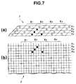
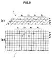
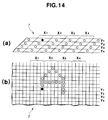
- Fig.14(a) shows openings of the control grid and (b) shows areas corresponding thereto on the transfer belt.
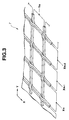
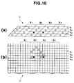
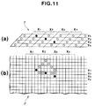
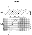
- the control grid has therein openings (XY %), each of which is a space (e.g., opening X N Y N enclosed by conductors X NL , X NR and Y NL , Y NR ) wherein an amount of toner passing therethrough is controlled by the action of the unit control electrodes (e.g., X N and Y N ) when the control voltage is applied thereto.
- openings XY (7), each of which is a space (e.g., opening X N Y N enclosed by conductors X NL , X NR and Y NL , Y NR ) wherein an amount of toner passing therethrough is controlled by the action of the unit control electrodes (e.g., X N and Y N ) when the control voltage is applied thereto.
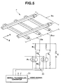
- a buffer/driver circuit 33 (Fig.5) provided, respectively, for each of the control units of X-electrodes and Y-electrodes is designed to select a controlled voltage of -100v at ON position and of -300v at OFF position according to an electric signal to be described later.
- this circuit is composed of a power source E, resistors R1 and R2, a transistor T1 and a photo-coupler P1.
Landscapes
- Physics & Mathematics (AREA)
- General Physics & Mathematics (AREA)
- Printers Or Recording Devices Using Electromagnetic And Radiation Means (AREA)
- Electrostatic Charge, Transfer And Separation In Electrography (AREA)
- Dot-Matrix Printers And Others (AREA)
- Electrophotography Using Other Than Carlson'S Method (AREA)
Priority Applications (1)
| Application Number | Priority Date | Filing Date | Title |
|---|---|---|---|
| EP96114841A EP0751443B1 (fr) | 1992-01-07 | 1992-12-23 | Appareil de formation d'images |
Applications Claiming Priority (2)
| Application Number | Priority Date | Filing Date | Title |
|---|---|---|---|
| JP4000588A JPH05177866A (ja) | 1992-01-07 | 1992-01-07 | 画像形成装置 |
| JP588/92 | 1992-01-07 |
Related Child Applications (2)
| Application Number | Title | Priority Date | Filing Date |
|---|---|---|---|
| EP96114841A Division EP0751443B1 (fr) | 1992-01-07 | 1992-12-23 | Appareil de formation d'images |
| EP96114841.8 Division-Into | 1996-09-16 |
Publications (3)
| Publication Number | Publication Date |
|---|---|
| EP0550880A2 true EP0550880A2 (fr) | 1993-07-14 |
| EP0550880A3 EP0550880A3 (fr) | 1993-08-04 |
| EP0550880B1 EP0550880B1 (fr) | 1997-04-02 |
Family
ID=11477889
Family Applications (2)
| Application Number | Title | Priority Date | Filing Date |
|---|---|---|---|
| EP92121856A Expired - Lifetime EP0550880B1 (fr) | 1992-01-07 | 1992-12-23 | Dispositif de formation d'images |
| EP96114841A Expired - Lifetime EP0751443B1 (fr) | 1992-01-07 | 1992-12-23 | Appareil de formation d'images |
Family Applications After (1)
| Application Number | Title | Priority Date | Filing Date |
|---|---|---|---|
| EP96114841A Expired - Lifetime EP0751443B1 (fr) | 1992-01-07 | 1992-12-23 | Appareil de formation d'images |
Country Status (4)
| Country | Link |
|---|---|
| US (1) | US5559586A (fr) |
| EP (2) | EP0550880B1 (fr) |
| JP (1) | JPH05177866A (fr) |
| DE (2) | DE69231341T2 (fr) |
Cited By (2)
| Publication number | Priority date | Publication date | Assignee | Title |
|---|---|---|---|---|
| EP0660201A3 (fr) * | 1993-12-27 | 1996-05-15 | Sharp Kk | Appareil de formation d'images. |
| US5585893A (en) * | 1994-06-22 | 1996-12-17 | Sharp Kabushiki Kaisha | Image forming apparatus |
Families Citing this family (32)
| Publication number | Priority date | Publication date | Assignee | Title |
|---|---|---|---|---|
| SE503955C2 (sv) * | 1994-09-19 | 1996-10-07 | Array Printers Ab | Metod och anordning för matning av tonerpartiklar i en printerenhet |
| WO1996018506A1 (fr) * | 1994-12-15 | 1996-06-20 | Array Printers Ab | Systeme d'impression en serie a depot direct de particules de poudre |
| JP3411434B2 (ja) * | 1994-12-27 | 2003-06-03 | シャープ株式会社 | 画像形成装置 |
| SE506483C2 (sv) | 1996-03-12 | 1997-12-22 | Ito Engineering Ab | Tryckverk av toner-jet typ |
| SE506484C2 (sv) | 1996-03-12 | 1997-12-22 | Ito Engineering Ab | Tryckverk av toner-jet-typ med elektriskt skärmad matris |
| US5971526A (en) * | 1996-04-19 | 1999-10-26 | Array Printers Ab | Method and apparatus for reducing cross coupling and dot deflection in an image recording apparatus |
| US5997133A (en) * | 1996-11-21 | 1999-12-07 | Nec Corporation | Inkjet recording apparatus having a minimum number of ejection electrode driving circuits and method for driving same |
| US5966152A (en) * | 1996-11-27 | 1999-10-12 | Array Printers Ab | Flexible support apparatus for dynamically positioning control units in a printhead structure for direct electrostatic printing |
| US5984456A (en) * | 1996-12-05 | 1999-11-16 | Array Printers Ab | Direct printing method utilizing dot deflection and a printhead structure for accomplishing the method |
| US6011944A (en) * | 1996-12-05 | 2000-01-04 | Array Printers Ab | Printhead structure for improved dot size control in direct electrostatic image recording devices |
| US6012801A (en) | 1997-02-18 | 2000-01-11 | Array Printers Ab | Direct printing method with improved control function |
| US6109730A (en) * | 1997-03-10 | 2000-08-29 | Array Printers Ab Publ. | Direct printing method with improved control function |
| US6017115A (en) * | 1997-06-09 | 2000-01-25 | Array Printers Ab | Direct printing method with improved control function |
| US6132029A (en) * | 1997-06-09 | 2000-10-17 | Array Printers Ab | Direct printing method with improved control function |
| JPH10337898A (ja) * | 1997-06-10 | 1998-12-22 | Sharp Corp | 画像形成装置 |
| US6257708B1 (en) | 1997-12-19 | 2001-07-10 | Array Printers Ab | Direct electrostatic printing apparatus and method for controlling dot position using deflection electrodes |
| US6086186A (en) * | 1997-12-19 | 2000-07-11 | Array Printers Ab | Apparatus for positioning a control electrode array in a direct electrostatic printing device |
| US6027206A (en) * | 1997-12-19 | 2000-02-22 | Array Printers Ab | Method and apparatus for cleaning the printhead structure during direct electrostatic printing |
| US6070967A (en) * | 1997-12-19 | 2000-06-06 | Array Printers Ab | Method and apparatus for stabilizing an intermediate image receiving member during direct electrostatic printing |
| US6209990B1 (en) | 1997-12-19 | 2001-04-03 | Array Printers Ab | Method and apparatus for coating an intermediate image receiving member to reduce toner bouncing during direct electrostatic printing |
| US6030070A (en) * | 1997-12-19 | 2000-02-29 | Array Printers Ab | Direct electrostatic printing method and apparatus |
| US6199971B1 (en) | 1998-02-24 | 2001-03-13 | Arrray Printers Ab | Direct electrostatic printing method and apparatus with increased print speed |
| US6074045A (en) * | 1998-03-04 | 2000-06-13 | Array Printers Ab | Printhead structure in an image recording device |
| US6174048B1 (en) | 1998-03-06 | 2001-01-16 | Array Printers Ab | Direct electrostatic printing method and apparatus with apparent enhanced print resolution |
| US6081283A (en) * | 1998-03-19 | 2000-06-27 | Array Printers Ab | Direct electrostatic printing method and apparatus |
| US6082850A (en) * | 1998-03-19 | 2000-07-04 | Array Printers Ab | Apparatus and method for controlling print density in a direct electrostatic printing apparatus by adjusting toner flow with regard to relative positioning of rows of apertures |
| US6102525A (en) * | 1998-03-19 | 2000-08-15 | Array Printers Ab | Method and apparatus for controlling the print image density in a direct electrostatic printing apparatus |
| EP0965455A1 (fr) | 1998-06-15 | 1999-12-22 | Array Printers Ab | Méthode et appareil d'impression électrostatique directe |
| ATE215238T1 (de) | 1998-06-15 | 2002-04-15 | Array Printers Ab | Verfahren und vorrichtung für direktes elektrostatisches drucken |
| JP2006095767A (ja) * | 2004-09-28 | 2006-04-13 | Fuji Photo Film Co Ltd | 画像形成装置 |
| EP1986054A1 (fr) * | 2007-04-24 | 2008-10-29 | AGC Flat Glass Europe SA | Unité de développement pour dispositif d'impression électrophotographique sur verre ou matériau en céramique |
| JP2013237245A (ja) * | 2012-05-17 | 2013-11-28 | Fuji Xerox Co Ltd | 画像記録装置 |
Family Cites Families (14)
| Publication number | Priority date | Publication date | Assignee | Title |
|---|---|---|---|---|
| JPS5741673A (en) * | 1980-08-25 | 1982-03-08 | Konishiroku Photo Ind Co Ltd | Copying device |
| JPH0647298B2 (ja) * | 1986-04-22 | 1994-06-22 | 富士ゼロックス株式会社 | 粉体画像記録方法 |
| US4690539A (en) * | 1986-05-27 | 1987-09-01 | Xerox Corporation | Transfer apparatus |
| SE459724B (sv) * | 1987-12-08 | 1989-07-31 | Larson Prod Ab Ove | Saett och anordning foer att framstaella ett latent elektriskt laddningsmoenster |
| US4780733A (en) * | 1987-12-31 | 1988-10-25 | Xerox Corporation | Printing apparatus and toner/developer delivery system therefor |
| SE8902090D0 (sv) * | 1989-06-07 | 1989-06-07 | Array Printers Ab | Saett att foerbaettra utskriftsprestanda foer skrivare samt anordningar foer genomfoerande av saettet |
| JPH03168767A (ja) * | 1989-11-29 | 1991-07-22 | Kyocera Corp | 画像形成方法 |
| JP2911045B2 (ja) * | 1989-11-29 | 1999-06-23 | 京セラ株式会社 | 画像形成装置 |
| US5374949A (en) * | 1989-11-29 | 1994-12-20 | Kyocera Corporation | Image forming apparatus |
| JP2968544B2 (ja) * | 1989-11-29 | 1999-10-25 | 京セラ株式会社 | 画像形成装置 |
| JP2930241B2 (ja) * | 1989-11-29 | 1999-08-03 | 京セラ株式会社 | 画像形成装置 |
| JP3080961B2 (ja) * | 1989-11-29 | 2000-08-28 | 京セラ株式会社 | 画像形成装置 |
| SE464284B (sv) * | 1990-01-03 | 1991-04-08 | Array Printers Ab | Saett att eliminera korskoppling mellan svaertningspunkter vid skrivare samt anordning foer genomfoerande av saettet |
| US5078087A (en) * | 1991-03-11 | 1992-01-07 | Xerox Corporation | Development apparatus |
-
1992
- 1992-01-07 JP JP4000588A patent/JPH05177866A/ja active Pending
- 1992-12-23 EP EP92121856A patent/EP0550880B1/fr not_active Expired - Lifetime
- 1992-12-23 EP EP96114841A patent/EP0751443B1/fr not_active Expired - Lifetime
- 1992-12-23 DE DE69231341T patent/DE69231341T2/de not_active Expired - Fee Related
- 1992-12-23 DE DE69218751T patent/DE69218751T2/de not_active Expired - Fee Related
-
1995
- 1995-11-21 US US08/561,142 patent/US5559586A/en not_active Expired - Fee Related
Cited By (3)
| Publication number | Priority date | Publication date | Assignee | Title |
|---|---|---|---|---|
| EP0660201A3 (fr) * | 1993-12-27 | 1996-05-15 | Sharp Kk | Appareil de formation d'images. |
| US5606402A (en) * | 1993-12-27 | 1997-02-25 | Sharp Kabushiki Kaisha | Electrostatic image former with improved toner control grid |
| US5585893A (en) * | 1994-06-22 | 1996-12-17 | Sharp Kabushiki Kaisha | Image forming apparatus |
Also Published As
| Publication number | Publication date |
|---|---|
| EP0751443B1 (fr) | 2000-08-09 |
| EP0751443A3 (fr) | 1997-01-15 |
| EP0550880B1 (fr) | 1997-04-02 |
| DE69218751T2 (de) | 1997-11-13 |
| DE69218751D1 (de) | 1997-05-07 |
| EP0550880A3 (fr) | 1993-08-04 |
| DE69231341D1 (de) | 2000-09-14 |
| DE69231341T2 (de) | 2001-02-01 |
| EP0751443A2 (fr) | 1997-01-02 |
| US5559586A (en) | 1996-09-24 |
| JPH05177866A (ja) | 1993-07-20 |
Similar Documents
| Publication | Publication Date | Title |
|---|---|---|
| US5559586A (en) | Image forming device having control grid with applied voltage of the same polarity as toner | |
| US5966151A (en) | Image forming apparatus | |
| JPH0630901B2 (ja) | 電荷潜像パターンを生成する方法およびこの方法を実施するための装置 | |
| CA1137539A (fr) | Imprimante electrophotographique a sources lumineuses multiples et variables en intensite | |
| EP0510963B1 (fr) | Méthode et appareil d'impression | |
| US5216453A (en) | Electrophotographic printer | |
| US5353050A (en) | Recording electrode for multicolor recording | |
| EP0717327B1 (fr) | Appareil de formation d'images comprenant chargement sélectif de toner appliqué à un support de toner | |
| US6154238A (en) | Scanning print head | |
| US6170935B1 (en) | Image forming apparatus that forms image on a medium by jumping developer | |
| JPH1076698A (ja) | 画像形成装置 | |
| US6056390A (en) | Image forming apparatus wherein the velocity of the toner supporting medium is higher than recording medium transport velocity | |
| US5655184A (en) | Ionographic printing with improved ion source | |
| US6270196B1 (en) | Tandem type of direct printing apparatus using gating apertures for supplying toner | |
| US4791494A (en) | Multiple variable light source printer | |
| JPH10337898A (ja) | 画像形成装置 | |
| JP3319936B2 (ja) | 画像形成装置 | |
| EP0860289A1 (fr) | Appareil de formation d'images | |
| JPH11320948A (ja) | 画像形成装置 | |
| JPH1142807A (ja) | 画像形成装置 | |
| JPH0920029A (ja) | 画像形成装置 | |
| US6270195B1 (en) | Image forming apparatus using gates and electrodes for selectively passing toner | |
| JPH11348340A (ja) | 飛翔型画像形成装置 | |
| JPH08142393A (ja) | 画像形成装置 | |
| JPH09207373A (ja) | 画像形成装置 |
Legal Events
| Date | Code | Title | Description |
|---|---|---|---|
| PUAI | Public reference made under article 153(3) epc to a published international application that has entered the european phase |
Free format text: ORIGINAL CODE: 0009012 |
|
| PUAL | Search report despatched |
Free format text: ORIGINAL CODE: 0009013 |
|
| AK | Designated contracting states |
Kind code of ref document: A2 Designated state(s): DE FR GB |
|
| AK | Designated contracting states |
Kind code of ref document: A3 Designated state(s): DE FR GB |
|
| 17P | Request for examination filed |
Effective date: 19931103 |
|
| 17Q | First examination report despatched |
Effective date: 19950207 |
|
| GRAG | Despatch of communication of intention to grant |
Free format text: ORIGINAL CODE: EPIDOS AGRA |
|
| GRAH | Despatch of communication of intention to grant a patent |
Free format text: ORIGINAL CODE: EPIDOS IGRA |
|
| GRAH | Despatch of communication of intention to grant a patent |
Free format text: ORIGINAL CODE: EPIDOS IGRA |
|
| GRAA | (expected) grant |
Free format text: ORIGINAL CODE: 0009210 |
|
| AK | Designated contracting states |
Kind code of ref document: B1 Designated state(s): DE FR GB |
|
| DX | Miscellaneous (deleted) | ||
| REF | Corresponds to: |
Ref document number: 69218751 Country of ref document: DE Date of ref document: 19970507 |
|
| ET | Fr: translation filed | ||
| PLBE | No opposition filed within time limit |
Free format text: ORIGINAL CODE: 0009261 |
|
| STAA | Information on the status of an ep patent application or granted ep patent |
Free format text: STATUS: NO OPPOSITION FILED WITHIN TIME LIMIT |
|
| 26N | No opposition filed | ||
| REG | Reference to a national code |
Ref country code: GB Ref legal event code: IF02 |
|
| PGFP | Annual fee paid to national office [announced via postgrant information from national office to epo] |
Ref country code: FR Payment date: 20061208 Year of fee payment: 15 |
|
| PGFP | Annual fee paid to national office [announced via postgrant information from national office to epo] |
Ref country code: GB Payment date: 20061220 Year of fee payment: 15 |
|
| PGFP | Annual fee paid to national office [announced via postgrant information from national office to epo] |
Ref country code: DE Payment date: 20061221 Year of fee payment: 15 |
|
| GBPC | Gb: european patent ceased through non-payment of renewal fee |
Effective date: 20071223 |
|
| PG25 | Lapsed in a contracting state [announced via postgrant information from national office to epo] |
Ref country code: DE Free format text: LAPSE BECAUSE OF NON-PAYMENT OF DUE FEES Effective date: 20080701 |
|
| REG | Reference to a national code |
Ref country code: FR Ref legal event code: ST Effective date: 20081020 |
|
| PG25 | Lapsed in a contracting state [announced via postgrant information from national office to epo] |
Ref country code: GB Free format text: LAPSE BECAUSE OF NON-PAYMENT OF DUE FEES Effective date: 20071223 |
|
| PG25 | Lapsed in a contracting state [announced via postgrant information from national office to epo] |
Ref country code: FR Free format text: LAPSE BECAUSE OF NON-PAYMENT OF DUE FEES Effective date: 20071231 |