EP0551648A2 - Procédé, système et carte pour le contrôle d'un équipement électronique, notamment d'une installations de télécommunications - Google Patents
Procédé, système et carte pour le contrôle d'un équipement électronique, notamment d'une installations de télécommunications Download PDFInfo
- Publication number
- EP0551648A2 EP0551648A2 EP92121871A EP92121871A EP0551648A2 EP 0551648 A2 EP0551648 A2 EP 0551648A2 EP 92121871 A EP92121871 A EP 92121871A EP 92121871 A EP92121871 A EP 92121871A EP 0551648 A2 EP0551648 A2 EP 0551648A2
- Authority
- EP
- European Patent Office
- Prior art keywords
- test
- board
- sequences
- computer
- bus
- Prior art date
- Legal status (The legal status is an assumption and is not a legal conclusion. Google has not performed a legal analysis and makes no representation as to the accuracy of the status listed.)
- Withdrawn
Links
- 238000012360 testing method Methods 0.000 title claims abstract description 92
- 238000000034 method Methods 0.000 title claims abstract description 16
- 230000004044 response Effects 0.000 claims description 23
- 230000015654 memory Effects 0.000 claims description 14
- 238000004891 communication Methods 0.000 claims description 6
- 238000010998 test method Methods 0.000 claims description 5
- 238000012545 processing Methods 0.000 claims description 3
- 235000000332 black box Nutrition 0.000 abstract description 3
- 229920001896 polybutyrate Polymers 0.000 description 7
- BHPFDLWDNJSMOS-UHFFFAOYSA-N 2-(9,10-diphenylanthracen-2-yl)-9,10-diphenylanthracene Chemical compound C1=CC=CC=C1C(C1=CC=C(C=C11)C=2C=C3C(C=4C=CC=CC=4)=C4C=CC=CC4=C(C=4C=CC=CC=4)C3=CC=2)=C(C=CC=C2)C2=C1C1=CC=CC=C1 BHPFDLWDNJSMOS-UHFFFAOYSA-N 0.000 description 2
- 230000000712 assembly Effects 0.000 description 2
- 238000000429 assembly Methods 0.000 description 2
- 230000000694 effects Effects 0.000 description 2
- 230000006399 behavior Effects 0.000 description 1
- 230000005540 biological transmission Effects 0.000 description 1
- 238000006243 chemical reaction Methods 0.000 description 1
- 238000007796 conventional method Methods 0.000 description 1
- 238000011990 functional testing Methods 0.000 description 1
- 230000010354 integration Effects 0.000 description 1
- 238000012552 review Methods 0.000 description 1
- 230000011664 signaling Effects 0.000 description 1
- 238000004088 simulation Methods 0.000 description 1
Images

Classifications
-
- G—PHYSICS
- G01—MEASURING; TESTING
- G01R—MEASURING ELECTRIC VARIABLES; MEASURING MAGNETIC VARIABLES
- G01R31/00—Arrangements for testing electric properties; Arrangements for locating electric faults; Arrangements for electrical testing characterised by what is being tested not provided for elsewhere
- G01R31/28—Testing of electronic circuits, e.g. by signal tracer
- G01R31/317—Testing of digital circuits
- G01R31/31712—Input or output aspects
- G01R31/31717—Interconnect testing
Definitions
- the present invention relates to a method,a system and a board for testing an electronic equipment, particularly a telecommunication equipment of the type comprising printed board assemblies interconnected through a bus and communicating each other in time division according to a predetermined protocol.
- PCM line monitors which de facto do not carry out any test but limit themselves to giving information on data travelling on such lines,are connected to the particular type of contemplated signalling.
- This object is achieved by the method of testing an electronic equipment having the characteristics set forth in claim 1, by the system having tie characteristics set forth in claim 8 and by the board having the characteristics set forth in claim 9.Further advantageous aspects of the present invention are set forth in the subclaims.
- PBAs printed Board Assemblies
- such boards are connected and communicate each other through a bus according to a well defined protocol; in case of telecommunication equipments, e.g. concentrators or exchange, the structure of such bus and the protocol correspond, as a rule,to a serial bus on which multiple PCM signals (24 or 32 channels) travel with a certain rate (64 Kbits/s, 2 Mbits/s, 4 Mbits/s).
- the complexity of the test is reduced and made independent of the architectural complexity of the electronic equipment: consequently a greater test completeness and also a greater test reliability can be obtained since the boards, each time tested, operate as if they were in the real working environment, i.e. the test is transparent to them.
- the interface being unique, a sole test system is sufficient by using different test sequences, of course.
- EE designates an electronic equipment, to which the test method and system according to the present invention are to be applied, comprising a number of boards PBA and a bus DB.
- the boards PBA are provided with an interface BI and are electrically connected with bus DB through such interface BI.
- the boards PBA communicate each other in time division according to a predetermined protocol.
- the method according to the present invention suggests to functionally test the boards PBA of the equipment EE one at a time through a suitable test system (TS, fig.2.) : the test of the equipment is then divided in a number, equal to the number of boards PBA, of board tests.
- TS test system
- test system (TS, fig.2) is connected to the board (PBAT, fig.2) to be tested through a test bus (TB, fig.2) structurally and functionally identical to the bus DB of the equipment, after having disconnected it (PBAT)from the latter (DB), or (TS) is connected to the equipment bus DB.
- the board test passes through the following steps :
- test system (TS, fig.2) be connected to the equipment bus DB, it is necessary to put first an addressing phase of the test board (PBAT, fig.2) before sending the sequence; such addressing phase can be merely composed of a temporary mechanical interruption of the activity of other boards not to be tested.
- memorization step a) will be preceded by a step of reception by the operator of the test sequence in a suitable format
- memorization step d) will be followed by a step of outputting the response sequence in a suitable format
- test sequences used in various cycles can be equal or different according to the board to be tested and the test strategy used.
- test sequences can be fixed in advance, before starting the test operation, or can be chosen during the test operation : e.g. the test sequence relative to a cycle can be chosen according to one or more response sequences relative to previous cycles.
- the preparation of the test sequences and the analysis of the response sequences can be also executed in an automatic manner, e.g. on the basis of technical specifications of the electronic equipment as a whole and of single boards.
- test system TS is connected through a test bus TB to a board to be tested PBAT of the electronic equipment EE shown in fig.1,or also to the case of testing an entire electronic equipment EE equipped with such an interface BI for its inputs and outputs.
- test system TS is connected to the bus DB of the equipment EE is anyhow structurally the same, as said.
- the board PBAT to be tested is equipped with an interface BI which test bus TB is connected to.
- test system TS comprised a computer PC adapted to memorize and process said test and response sequences,and a test board PBA electrically connected to computer PC and designed to receive from computer PC test sequences and retransmit them on test bus TB,to receive from test bus TB response sequences,and retransmit them to computer PC, and to receive and transmit control commands from and to computer PC.
- test board TBA is conceptually composed of:
- Sending of a test sequence and reception of said response sequence occur, according to the cases already seen, either over the bus DB of the equipment EE or over the test bus TB.
- connection of interface CI with the two interfaces OI and II must be considered as logic ones since such sequences follow the above-mentioned paths;they may correspond also to real electrical paths but there is nothing to prevent the device from executing processes on them and therefore the physical paths from passing through such device.
- timing signal occurs, as a rule, from one of the two busses. Sometimes such a signal can be obtained from signals travelling over the bus itself. Very often at least a timing signal is contemplated in the bus : in case of computers it is known as clock, in case of serial busses for multichannel PCM signals there are two timing signals, one for the bit and one for identifying the frame beginnings.
- Computer PC is advantageously a personal computer ; in this case, given the relative simplicity of the remaining circuitry, which is often realized with broad use of integrated circuits,the remaining circuitry can be located on a test board TPBA to be connected directly to the bus of the personal computer : interface CI to the computer shall be then a well known interface for personal computer bus.
- signals travelling over the bus can be of the type multichannel PCM or V24,in which case input interface II and output interface OI must be adapted to operate on such kind of signals : circuital solutions suitable for realizing them can be found in circuits of the boards PBA of the equipment to be tested.
- interfaces II and OI are provided with internal memories designed to memorize data temporarily.
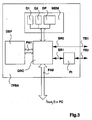
- Such board consists essentially of a communication processor QRC,electrically connected to a random access memory MEM.
- a processor QRC is described in the European Patent Application EP91120547 and contains inside it,in an its integrated embodiment,two serial interfaces (having inputs/outputs SRO and SR1)of type multichannel PCM,two parallel interfaces (having inputs/outputs PA0 and PA1),an interface for the connection with an external memory, a control device and an internal memory.
- Processor QRC is able to configurate memory MEM as a number of independent memory blocks of various types,e.g. FIFO,LIFO,circular queue,multipoint memory.
- Connected with one of the parallel ports,PA0 in fig.3, is a processor,computer PC in fig.3,able to control and determine the behaviour of processor QRC.
- memory MEM is configurated as two FIFO memory blocks Q1 and Q2 also called queues:and the processor QRC accumulates in queue Q1 the test sequences as they are received by computer PC and in queue Q2 the response sequences as they are received by one of the serial ports SR0 and SR1.
- the handling of queues Q1 and Q2 is completely under the control of processor QRC as far as write and read out are concerned.
- the choice of the serial port is carried out through sending of suitable commands by computer PC.
- a protocol interface PI able to convert the multichannel PCM signal into a type V24 signal.Therefore the choice of the two ports depends on the electronic equipments to be tested.
- a digital signal processor DSP can be electrically connected to the second parallel port PA1 to operate digital processing on the test sequences to be transmitted and on the received response sequences.
- the computer PC transfers the program to be processed by processor DSP; moreover,processor DSP uses the remaining cells of block DP,not occupied by the program,as working storage.
Landscapes
- Engineering & Computer Science (AREA)
- General Engineering & Computer Science (AREA)
- Physics & Mathematics (AREA)
- General Physics & Mathematics (AREA)
- Test And Diagnosis Of Digital Computers (AREA)
Applications Claiming Priority (4)
| Application Number | Priority Date | Filing Date | Title |
|---|---|---|---|
| ITMI920060 | 1992-01-15 | ||
| ITMI920060A IT1258771B (it) | 1992-01-15 | 1992-01-15 | Metodo e sistema per testare una apparecchiatura elettronica in particolare per telecomunicazioni |
| ITMI922121 | 1992-09-15 | ||
| ITMI922121A IT1255599B (it) | 1992-09-15 | 1992-09-15 | Metodo, sistema e piastra per testare una apparecchiatura elettronica in particolare per telecomunicazioni |
Publications (2)
| Publication Number | Publication Date |
|---|---|
| EP0551648A2 true EP0551648A2 (fr) | 1993-07-21 |
| EP0551648A3 EP0551648A3 (en) | 1993-12-08 |
Family
ID=26330820
Family Applications (1)
| Application Number | Title | Priority Date | Filing Date |
|---|---|---|---|
| EP19920121871 Withdrawn EP0551648A3 (en) | 1992-01-15 | 1992-12-23 | Method of, system and board for testing an electronic equipment, particularly a telecommunication equipment |
Country Status (1)
| Country | Link |
|---|---|
| EP (1) | EP0551648A3 (fr) |
Cited By (1)
| Publication number | Priority date | Publication date | Assignee | Title |
|---|---|---|---|---|
| US5787147A (en) * | 1995-12-21 | 1998-07-28 | Ericsson Inc. | Test message generator in a telecommunications network |
Family Cites Families (2)
| Publication number | Priority date | Publication date | Assignee | Title |
|---|---|---|---|---|
| US4176780A (en) * | 1977-12-06 | 1979-12-04 | Ncr Corporation | Method and apparatus for testing printed circuit boards |
| GB2189890B (en) * | 1986-04-30 | 1990-02-14 | Plessey Co Plc | A unit for testing digital telecommunications exchange equipment |
-
1992
- 1992-12-23 EP EP19920121871 patent/EP0551648A3/en not_active Withdrawn
Cited By (1)
| Publication number | Priority date | Publication date | Assignee | Title |
|---|---|---|---|---|
| US5787147A (en) * | 1995-12-21 | 1998-07-28 | Ericsson Inc. | Test message generator in a telecommunications network |
Also Published As
| Publication number | Publication date |
|---|---|
| EP0551648A3 (en) | 1993-12-08 |
Similar Documents
| Publication | Publication Date | Title |
|---|---|---|
| CA2082608C (fr) | Reseau de commutation telephonique milticanal a formats de signalisation multiples et a interconnexion selectionnable pour chaque canal | |
| US4955054A (en) | Integrated telecommunication system with improved digital voice response | |
| US4525830A (en) | Advanced network processor | |
| CA1065977A (fr) | Reseau de commutation pour reseau pcm tdm | |
| CA1171946A (fr) | Matrice de commutation a repartition dans le temps | |
| CA1203875A (fr) | Circuit de retour pour verifier un systeme de commutation | |
| US5592653A (en) | Interface conversion device | |
| GB1582583A (en) | Digital switching arrangements for stored programme control telecommunications systems | |
| EP0419750B1 (fr) | Mécanisme de distribution pour établir des communications entre des interfaces d'utilisateur d'un système de communication | |
| EP0551648A2 (fr) | Procédé, système et carte pour le contrôle d'un équipement électronique, notamment d'une installations de télécommunications | |
| GB1581838A (en) | I/o bus transceiver for a data processing system | |
| CA1121894A (fr) | Multiplexeur decodeur de supervision de circuit digital pour le declenchement par la terre ou la signalisation par fils e et m sur une portee commune t1 | |
| US4493073A (en) | Maintenance of stored program controlled switching systems | |
| US4347601A (en) | Method and system for processing coded information transmitted during cyclically successive time frames | |
| US4509168A (en) | Digital remote switching unit | |
| US4532624A (en) | Parity checking arrangement for a remote switching unit network | |
| JPS5814120B2 (ja) | 時分割交換センタ用信号転送方式 | |
| RU2775703C1 (ru) | Многоканальное устройство межмашинного прямого доступа к памяти | |
| US4905236A (en) | Circuit arrangement for designational reading of information of a bit group oriented, continuous information stream at an ISDN-oriented interface | |
| US4514842A (en) | T-S-T-S-T Digital switching network | |
| EP0369116B1 (fr) | Commande de matrice de commutation MRT | |
| EP0351959A2 (fr) | Commande de canaux multiples | |
| EP0260793A2 (fr) | Bus bidirectionnel de données | |
| JP2521957B2 (ja) | 伝送システム | |
| US4127745A (en) | Date time-multiplex switching network for use in a telecommunications exchange |
Legal Events
| Date | Code | Title | Description |
|---|---|---|---|
| PUAI | Public reference made under article 153(3) epc to a published international application that has entered the european phase |
Free format text: ORIGINAL CODE: 0009012 |
|
| AK | Designated contracting states |
Kind code of ref document: A2 Designated state(s): BE DE ES FR GB IT NL SE |
|
| PUAL | Search report despatched |
Free format text: ORIGINAL CODE: 0009013 |
|
| AK | Designated contracting states |
Kind code of ref document: A3 Designated state(s): BE DE ES FR GB IT NL SE |
|
| STAA | Information on the status of an ep patent application or granted ep patent |
Free format text: STATUS: THE APPLICATION IS DEEMED TO BE WITHDRAWN |
|
| 18D | Application deemed to be withdrawn |
Effective date: 19940609 |