EP0554825B1 - Direktkontakt-Bildsensor und Herstellungsverfahren dafür - Google Patents
Direktkontakt-Bildsensor und Herstellungsverfahren dafür Download PDFInfo
- Publication number
- EP0554825B1 EP0554825B1 EP93101546A EP93101546A EP0554825B1 EP 0554825 B1 EP0554825 B1 EP 0554825B1 EP 93101546 A EP93101546 A EP 93101546A EP 93101546 A EP93101546 A EP 93101546A EP 0554825 B1 EP0554825 B1 EP 0554825B1
- Authority
- EP
- European Patent Office
- Prior art keywords
- image sensor
- optical fiber
- fiber array
- transparent
- direct contact
- Prior art date
- Legal status (The legal status is an assumption and is not a legal conclusion. Google has not performed a legal analysis and makes no representation as to the accuracy of the status listed.)
- Expired - Lifetime
Links
Images




Classifications
-
- H—ELECTRICITY
- H04—ELECTRIC COMMUNICATION TECHNIQUE
- H04N—PICTORIAL COMMUNICATION, e.g. TELEVISION
- H04N1/00—Scanning, transmission or reproduction of documents or the like, e.g. facsimile transmission; Details thereof
- H04N1/024—Details of scanning heads ; Means for illuminating the original
- H04N1/028—Details of scanning heads ; Means for illuminating the original for picture information pick-up
- H04N1/03—Details of scanning heads ; Means for illuminating the original for picture information pick-up with photodetectors arranged in a substantially linear array
- H04N1/031—Details of scanning heads ; Means for illuminating the original for picture information pick-up with photodetectors arranged in a substantially linear array the photodetectors having a one-to-one and optically positive correspondence with the scanned picture elements, e.g. linear contact sensors
- H04N1/0311—Details of scanning heads ; Means for illuminating the original for picture information pick-up with photodetectors arranged in a substantially linear array the photodetectors having a one-to-one and optically positive correspondence with the scanned picture elements, e.g. linear contact sensors using an array of elements to project the scanned image elements onto the photodetectors
- H04N1/0312—Details of scanning heads ; Means for illuminating the original for picture information pick-up with photodetectors arranged in a substantially linear array the photodetectors having a one-to-one and optically positive correspondence with the scanned picture elements, e.g. linear contact sensors using an array of elements to project the scanned image elements onto the photodetectors using an array of optical fibres or rod-lenses
-
- H—ELECTRICITY
- H04—ELECTRIC COMMUNICATION TECHNIQUE
- H04N—PICTORIAL COMMUNICATION, e.g. TELEVISION
- H04N1/00—Scanning, transmission or reproduction of documents or the like, e.g. facsimile transmission; Details thereof
- H04N1/00519—Constructional details not otherwise provided for, e.g. housings, covers
- H04N1/00557—Connection or assembly of components or elements
-
- H—ELECTRICITY
- H04—ELECTRIC COMMUNICATION TECHNIQUE
- H04N—PICTORIAL COMMUNICATION, e.g. TELEVISION
- H04N1/00—Scanning, transmission or reproduction of documents or the like, e.g. facsimile transmission; Details thereof
- H04N1/024—Details of scanning heads ; Means for illuminating the original
- H04N1/028—Details of scanning heads ; Means for illuminating the original for picture information pick-up
- H04N1/03—Details of scanning heads ; Means for illuminating the original for picture information pick-up with photodetectors arranged in a substantially linear array
- H04N1/031—Details of scanning heads ; Means for illuminating the original for picture information pick-up with photodetectors arranged in a substantially linear array the photodetectors having a one-to-one and optically positive correspondence with the scanned picture elements, e.g. linear contact sensors
- H04N1/0311—Details of scanning heads ; Means for illuminating the original for picture information pick-up with photodetectors arranged in a substantially linear array the photodetectors having a one-to-one and optically positive correspondence with the scanned picture elements, e.g. linear contact sensors using an array of elements to project the scanned image elements onto the photodetectors
-
- H—ELECTRICITY
- H04—ELECTRIC COMMUNICATION TECHNIQUE
- H04N—PICTORIAL COMMUNICATION, e.g. TELEVISION
- H04N1/00—Scanning, transmission or reproduction of documents or the like, e.g. facsimile transmission; Details thereof
- H04N1/024—Details of scanning heads ; Means for illuminating the original
- H04N1/028—Details of scanning heads ; Means for illuminating the original for picture information pick-up
- H04N1/03—Details of scanning heads ; Means for illuminating the original for picture information pick-up with photodetectors arranged in a substantially linear array
- H04N1/031—Details of scanning heads ; Means for illuminating the original for picture information pick-up with photodetectors arranged in a substantially linear array the photodetectors having a one-to-one and optically positive correspondence with the scanned picture elements, e.g. linear contact sensors
- H04N1/0315—Details of scanning heads ; Means for illuminating the original for picture information pick-up with photodetectors arranged in a substantially linear array the photodetectors having a one-to-one and optically positive correspondence with the scanned picture elements, e.g. linear contact sensors using photodetectors and illumination means mounted on separate supports or substrates or mounted in different planes
- H04N1/0316—Details of scanning heads ; Means for illuminating the original for picture information pick-up with photodetectors arranged in a substantially linear array the photodetectors having a one-to-one and optically positive correspondence with the scanned picture elements, e.g. linear contact sensors using photodetectors and illumination means mounted on separate supports or substrates or mounted in different planes illuminating the scanned image elements through the plane of the photodetector, e.g. back-light illumination
-
- H—ELECTRICITY
- H10—SEMICONDUCTOR DEVICES; ELECTRIC SOLID-STATE DEVICES NOT OTHERWISE PROVIDED FOR
- H10F—INORGANIC SEMICONDUCTOR DEVICES SENSITIVE TO INFRARED RADIATION, LIGHT, ELECTROMAGNETIC RADIATION OF SHORTER WAVELENGTH OR CORPUSCULAR RADIATION
- H10F39/00—Integrated devices, or assemblies of multiple devices, comprising at least one element covered by group H10F30/00, e.g. radiation detectors comprising photodiode arrays
- H10F39/80—Constructional details of image sensors
Definitions
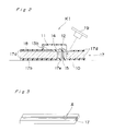
- the optical fiber array plate 17 includes a transparent substrate 17b, an optical fiber array 15, light shielding layers 17d formed on upper and lower faces of the transparent substrate 17b and a transparent resinous layer 17e formed on the lower face of the transparent substrate 17b such that the transparent resinous layer 17e is brought into close contact with an original document 10.
- the flexible circuit conductive substrate 38b is bonded to the transparent substrate 37b of the optical fiber array plate 37 with transparent insulating resin such as phenol epoxy resin, epoxy resin, etc. by using a press so as to extend flat relative to the transparent substrate 37b without being curved.
- transparent insulating resin such as phenol epoxy resin, epoxy resin, etc.
- this transparent insulating resin desirably has a thickness of not more than 50 ⁇ m, preferably, 10 to 25 ⁇ m.
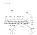
- a thin glass sheet of about 50 ⁇ m in thickness on which a transparent electrode is formed as the transparent conductive layer 47e may be used as the transparent film substrate 47c. Since the transparent film substrate 47c which is brought into contact with an original document 40 is required to have a high flatness, the transparent film substrate 47c is secured to the translucent carrier 47f through the carrier 47h and is fixed to the semiconductor image sensor chip 41 through the transparent resin 44b.
- the transparent resin 44b may be (a) silicone type or acrylic type photo-setting resin, (b) thermosetting resin or (c) resin setting at room temperature.
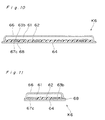
- Figs. 10 and 11 show a direct contact type image sensor K6 employing a transparent film substrate 67c, according to a sixth embodiment of the present invention.
- the image sensor K6 includes circuit conductive layers 68 formed on the upper face of the transparent film substrate 67c, a semiconductor image sensor chip 61 acting as a semiconductor device, bump electrodes 63b provided on the semiconductor image sensor chip 61, a transparent photo-setting and insulating resin 64 for mounting the semiconductor image sensor chip 61 on the transparent film substrate 67c, a transparent protective layer 66 for protecting the semiconductor image sensor chip 61 and a photosensor array 62 provided in the semiconductor image sensor chip 61.
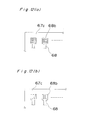
- a portion 68b of each of the circuit conductive layers 68 is brought into contact with the corresponding bump electrode 63b and may have a latticed shape and a forked shape as shown in Figs. 12(a) and 12(b), respectively.
- the transparent film substrate 67c made of polyallylate (PA), polyether sulfone (PES), polyethylene terephthalate (PET), etc.
- metal such as copper is formed by deposition method or sputtering method or by using a foil and then, is subjected to photolithography.
- the circuit conductive layers 68 are obtained.
- a preset amount of the acrylate type transparent photo-setting and insulating resin 64 is applied to a predetermined location of the transparent film substrate 67c by stamping method or screen printing method. Then, the semiconductor image sensor chip 61 is placed in face-down orientation such that the bump electrode 63b is brought into contact with the corresponding circuit conductive layer 68.
- the transparent photo-setting and insulating resin 64 be made of urethane acrylate type resin or epoxy acrylate type resin.
- the transparent photo-setting and insulating resin 64 covered by the circuit conductive layers 68 is set securely and electrical connection of the semiconductor image sensor chip 61 is improved.
- the image sensor K6 is resistant against combination of a high temperature of 85 °C and a high humidity of 85 %, a high temperature of 85 °C, a low temperature of -40 °C and thermal shocks ranging from -40 °C to 85 °C and thus, has high reliability sufficient for practical use.
- Figs. 13 and 14 show an image sensor K7 employing a transparent film substrate 77c, according to a seventh embodiment of the present invention.
- the image sensor K7 includes a circuit conductive layer 78 formed on the upper face of the transparent film substrate 77c, a semiconductor image sensor chip 71, a bump electrode 73b provided on the semiconductor image sensor chip 71, transparent photo-setting and insulating resin 74 for mounting the semiconductor image sensor chip 71 on the transparent film substrate 77c, a transparent protective layer 76 for protecting the semiconductor image sensor chip 71, a photosensor array 72 provided in the semiconductor image sensor chip 71 and light shielding layers 71b and 77c.
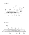
- Figs. 15 and 16 show construction of the semiconductor image sensor chip 71.
- the transparent film substrate 77c has a thickness of 25 to 200 ⁇ m and is formed by a sheet of polyallylate (PA), polyether sulfone (PES), polyethylene terephthalate (PET), etc.
- Metal such as copper or the like is formed on the upper face of the transparent film substrate 77c to a thickness of 2 to 20 ⁇ m by deposition method or sputtering method or by using a foil and then, is subjected to photolithography. As a result, the circuit conductive layer 78 is obtained.
- a preset amount of the acrylate type transparent photo-setting and insulating resin 74 is applied to a predetermined location of the transparent film substrate 77c by stamping method or screen printing method.
- the semiconductor image sensor chip 71 is placed in face-down orientation such that the bump electrode 73b is brought into contact with the corresponding circuit conductive layer 78. Subsequently, while a predetermined pressure is being applied to the semiconductor image sensor chip 71 from above, light is irradiated to the transparent photo-setting and insulating resin 74 through the transparent film substrate 77c so as to set the transparent photo-setting and insulating resin 74. Thereafter, by applying resin, e.g., transparent silicone resin to the semiconductor image sensor chip 71 with a dispenser, the transparent protective layer 76 is formed. From a standpoint of bonding property and optical sensitivity, it is desirable that the transparent photo-setting and insulating resin 74 be made of urethane acrylate type resin or epoxy acrylate type resin.
- the lower face of the transparent film substrate 77c is brought into close contact with an original document 70 and the original document 70 is illuminated from above by a LED array 79 through a slit formed by the semiconductor image sensor chip 71 and the light shielding layer 71b, the transparent protective layer 76, the transparent photo-setting and insulating resin 74 and the transparent film substrate 77c. Then, optical data from the original document 70 is directly fed to the photosensor array 72 through the transparent film substrate 77c and the transparent photo-setting and insulating resin 74 such that information of the original document is read.
- optical data from the original document 70 can be read by the image sensor K7 without the need for providing a lens system and without optical crosstalk by the light shielding layer 77d at high resolution in which an MTF has a value of 50 % for a chart having 4 line pairs/mm but the image sensor K7 itself can be remarkably reduced in size.
Landscapes
- Engineering & Computer Science (AREA)
- Multimedia (AREA)
- Signal Processing (AREA)
- Facsimile Heads (AREA)
Claims (11)
- Direktkontakt-Bildsensor (K1) mit:gekennzeichnet durcheiner Platte (17, 37) mit einer Anordnung optischer Fasern, welche ein transparentes Substrat (17b, 37b) und eine Anordnung (15) optischer Fasern einschließt, die in das transparente Substrat eingeschmolzen sind, und welche Ober- und Unterseiten aufweist, derart daß die Unterseite der Platte mit einer Anordnung optischer Fasern in dichten Kontakt mit einem Originaldokument (10) gebracht werden kann;wobei die Anordnung (15) optischer Fasern durch mindestens eine Vielzahl von optischen Fasern (15a) gebildet ist, welche in einer Reihe angeordnet sind, und wobei die optischen Fasern (15a) jeweils einen in ihrer Mitte angeordneten Kern (15b), eine Hülle (15c), welche den Kern (15b) umgibt, und einen optischen Absorber (15d), welcher die Hülle (15c) beschichtet, enthält;einem Halbleiterbildsensorchip (11), welcher eine Fotosensoranordnung (12) aufweist, und auf der Oberseite der Platte (17, 37) mit einer Anordnung optischer Fasern angebracht ist, derart daß die Fotosensoranordnung (12) optisch mit einer Unterseite der Anordnung (15) optischer Fasern durch die Anordnung optischer Fasern verbunden ist;einer elektrisch leitenden Leitungsschicht (18), welche auf einer Oberseite des transparenten Substrates (17b, 37b) angeordnet ist;einer Anschlußelektrode (13b), welche auf einer Unterseite des Halbleiterbildsensorschips (11) angebracht ist, um so in Kontakt mit der elektrisch leitenden Leitungsschicht (18) zu kommen;einer Lichtquelle (19) zum Beleuchten des Originaldokuments (10);eine erste Lichtabschirmschicht (17d), welche an anderen Abschnitten der Unterseite der Platte (17) mit einer Anordnung optischer Fasern angeordnet sind als jene, die der Anordnung (15) optischer Fasern entsprechen; undeine zweite Lichtabschirmschicht (17d), welche an anderen Abschnitten der Oberseite der Platte (17) mit einer Anordnung optischer Fasern angeordnet sind als jene, die der Anordnung (15) optischer Fasern entsprechen, und einen Schlitz, um es dem Licht der Lichtquelle (19) zu erlauben, dort hindurchzutreten;wobei der Halbleiterbildsensorchip (11) auf der Oberseite der Platte (17) mit einer Anordnung optischer Fasern durch transparenten Fotosatz und isolierendes Harz (14) angebracht ist.
- Direktkontakt-Bildsensor (K1) nach Anspruch 1, weiterhin enthaltend:
eine transparente harzige Schicht (17e), welche über die gesamte Unterseite der Platte (17) mit einer Anordnung optischer Fasern angeordnet ist. - Direktkontakt-Bildsensor (K1) nach Anspruch 2, wobei die transparente harzige Schicht (17e) einen Brechungsindex gleich dem des Kerns (15b) jedes der optischen Fasern (15a) aufweist.
- Direktkontakt-Bildsensor (K1) nach Anspruch 2, wobei die transparente harzige Schicht (17e) und die erste Lichtabschirmschicht (17d) eine Bleistifthärte von nicht weniger als 3H aufweisen.
- Direktkontakt-Bildsensor (K3) nach den Ansprüchen 1 oder 2, weiterhin enthaltend:
eine dritte Lichtabschirmschicht (37d), welche auf einer gesamten Seitenfläche der Platte (37) mit einer Anordnung optischer Fasern angeordnet ist. - Direktkontakt-Bildsensor (K1) nach Anspruch 1, wobei die leitende Leitungsschicht (18) durch ein Dickschichtdruckverfahren gebildet ist.
- Direktkontakt-Bildsensor (K1) nach Anspruch 1, wobei die leitende Leitungsschicht (18) durch ein Dünnschichtdruckverfahren gebildet ist.
- Direktkontakt-Bildsensor (K3) nach Anspruch 1, wobei die elektrische Leitungsschicht (18) durch ein flexibles, leitendes Leitungssubstrat (38b) gebildet ist.
- Direktkontakt-Bildsensor (K3) nach Anspruch 8, wobei die Anschlußelektrode (33b) für das flexible, leitende Leitungssubstrat (38b) eine Höhe von nicht mehr als 100 µm aufweist.
- Direktkontakt-Bildsensor (K1) nach Anspruch 1, wobei die Lichtquelle (19) oberhalb der Oberseite der Platte (17) mit einer Anordnung optischer Fasern angeordnet ist, und das Licht von der Lichtquelle (19) durch die Hülle (15c) von dem optischen Absorber (15d) auf den Kern (15b) auftrifft, um so auf das Originaldokument (10) durch die Platte (17) mit einer Anordnung optischer Fasern gestrahlt zu werden.
- Direktkontakt-Bildsensor (K3) nach Anspruch 10, weiterhin enthaltend: eine Transportwalze (30b) zum Zuführen des Originaldokuments (30) in eine Ausleseposition eines Lesegerätes;wobei reflektiertes Licht von dem Originaldokument, welches durch die Lichtquelle (39) eingestrahlt wird, zu der Fotosensoranordnung (32) geführt wird, um in ein elektrisches Signal umgewandelt zu werden, so daß ein Bild des Originaldokuments (30) gelesen wird;wobei die Transportwalze (30b) aus elektrisch leitfähigem Gummi mit einem Flächenwiderstand von nicht mehr als 107 Ω/□ gebildet ist.
Applications Claiming Priority (6)
| Application Number | Priority Date | Filing Date | Title |
|---|---|---|---|
| JP18615/92 | 1992-02-04 | ||
| JP4018615A JPH0630191A (ja) | 1992-02-04 | 1992-02-04 | 密着型イメージセンサ及びイメージセンサユニット |
| JP99240/92 | 1992-04-20 | ||
| JP4099240A JPH05300323A (ja) | 1992-04-20 | 1992-04-20 | 画像読み取り装置 |
| JP264511/92 | 1992-10-02 | ||
| JP4264511A JPH06121112A (ja) | 1992-10-02 | 1992-10-02 | 密着型イメージセンサの製造方法およびイメージセンサユニット |
Publications (2)
| Publication Number | Publication Date |
|---|---|
| EP0554825A1 EP0554825A1 (de) | 1993-08-11 |
| EP0554825B1 true EP0554825B1 (de) | 1998-10-28 |
Family
ID=27282290
Family Applications (1)
| Application Number | Title | Priority Date | Filing Date |
|---|---|---|---|
| EP93101546A Expired - Lifetime EP0554825B1 (de) | 1992-02-04 | 1993-02-02 | Direktkontakt-Bildsensor und Herstellungsverfahren dafür |
Country Status (4)
| Country | Link |
|---|---|
| US (1) | US5835142A (de) |
| EP (1) | EP0554825B1 (de) |
| KR (1) | KR970011025B1 (de) |
| DE (1) | DE69321745T2 (de) |
Families Citing this family (50)
| Publication number | Priority date | Publication date | Assignee | Title |
|---|---|---|---|---|
| KR0125137B1 (ko) * | 1993-10-14 | 1997-12-01 | 미타라이 하지메 | 밀착형 이미지센서 |
| US6654064B2 (en) * | 1997-05-23 | 2003-11-25 | Canon Kabushiki Kaisha | Image pickup device incorporating a position defining member |
| US6090687A (en) * | 1998-07-29 | 2000-07-18 | Agilent Technolgies, Inc. | System and method for bonding and sealing microfabricated wafers to form a single structure having a vacuum chamber therein |
| JP4197217B2 (ja) * | 2000-05-08 | 2008-12-17 | 株式会社半導体エネルギー研究所 | 装置 |
| EP1158775A1 (de) | 2000-05-15 | 2001-11-28 | EASTMAN KODAK COMPANY (a New Jersey corporation) | Bildaufnahmevorrichtung mit integrierter Farbbeleuchtung |
| US6669802B2 (en) * | 2000-12-21 | 2003-12-30 | Spenco | Composite riser |
| FR2819103B1 (fr) * | 2000-12-29 | 2003-12-12 | St Microelectronics Sa | Boitier semi-conducteur optique a pastille transparente et son procede de fabrication |
| IL159113A (en) * | 2002-11-27 | 2008-11-26 | Given Imaging Ltd | Method and device of imaging with an imager having a fiber plate cover |
| US7275292B2 (en) * | 2003-03-07 | 2007-10-02 | Avago Technologies Wireless Ip (Singapore) Pte. Ltd. | Method for fabricating an acoustical resonator on a substrate |
| US7191662B2 (en) * | 2003-06-09 | 2007-03-20 | Motorola, Inc. | Polymer-based sensor apparatus and method |
| US7294919B2 (en) * | 2003-11-26 | 2007-11-13 | Avago Technologies General Ip (Singapore) Pte. Ltd. | Device having a complaint element pressed between substrates |
| US7615833B2 (en) * | 2004-07-13 | 2009-11-10 | Avago Technologies Wireless Ip (Singapore) Pte. Ltd. | Film bulk acoustic resonator package and method of fabricating same |
| US7811961B2 (en) * | 2004-08-12 | 2010-10-12 | Ford Global Technologies, Llc | Methods and formulations for enhancing NH3 adsorption capacity of selective catalytic reduction catalysts |
| US7388454B2 (en) | 2004-10-01 | 2008-06-17 | Avago Technologies Wireless Ip Pte Ltd | Acoustic resonator performance enhancement using alternating frame structure |
| US8981876B2 (en) | 2004-11-15 | 2015-03-17 | Avago Technologies General Ip (Singapore) Pte. Ltd. | Piezoelectric resonator structures and electrical filters having frame elements |
| US7202560B2 (en) | 2004-12-15 | 2007-04-10 | Avago Technologies Wireless Ip (Singapore) Pte. Ltd. | Wafer bonding of micro-electro mechanical systems to active circuitry |
| US7791434B2 (en) | 2004-12-22 | 2010-09-07 | Avago Technologies Wireless Ip (Singapore) Pte. Ltd. | Acoustic resonator performance enhancement using selective metal etch and having a trench in the piezoelectric |
| US7369013B2 (en) | 2005-04-06 | 2008-05-06 | Avago Technologies Wireless Ip Pte Ltd | Acoustic resonator performance enhancement using filled recessed region |
| FR2888043B1 (fr) * | 2005-07-01 | 2007-11-30 | Atmel Grenoble Soc Par Actions | Capteur d'image a galette de fibres optiques |
| US7737807B2 (en) | 2005-10-18 | 2010-06-15 | Avago Technologies Wireless Ip (Singapore) Pte. Ltd. | Acoustic galvanic isolator incorporating series-connected decoupled stacked bulk acoustic resonators |
| TW200729364A (en) * | 2006-01-26 | 2007-08-01 | Ind Tech Res Inst | Circuit substrate and packaging thereof and method for fabricating the packaging |
| US7746677B2 (en) | 2006-03-09 | 2010-06-29 | Avago Technologies Wireless Ip (Singapore) Pte. Ltd. | AC-DC converter circuit and power supply |
| US7479685B2 (en) | 2006-03-10 | 2009-01-20 | Avago Technologies General Ip (Singapore) Pte. Ltd. | Electronic device on substrate with cavity and mitigated parasitic leakage path |
| US20080180389A1 (en) * | 2007-01-26 | 2008-07-31 | Michael Kelly | Optical-based interconnect for integrated circuits and related system and method |
| US8320704B2 (en) * | 2007-09-21 | 2012-11-27 | Gatan, Inc. | Method for creating reference images in electron microscopes |
| US7732977B2 (en) | 2008-04-30 | 2010-06-08 | Avago Technologies Wireless Ip (Singapore) | Transceiver circuit for film bulk acoustic resonator (FBAR) transducers |
| US7855618B2 (en) | 2008-04-30 | 2010-12-21 | Avago Technologies Wireless Ip (Singapore) Pte. Ltd. | Bulk acoustic resonator electrical impedance transformers |
| CN102308208B (zh) * | 2008-12-23 | 2014-12-03 | 3M创新有限公司 | 具有微孔有机硅酸盐材料的有机化学传感器 |
| US8248185B2 (en) | 2009-06-24 | 2012-08-21 | Avago Technologies Wireless Ip (Singapore) Pte. Ltd. | Acoustic resonator structure comprising a bridge |
| US8902023B2 (en) | 2009-06-24 | 2014-12-02 | Avago Technologies General Ip (Singapore) Pte. Ltd. | Acoustic resonator structure having an electrode with a cantilevered portion |
| US8193877B2 (en) | 2009-11-30 | 2012-06-05 | Avago Technologies Wireless Ip (Singapore) Pte. Ltd. | Duplexer with negative phase shifting circuit |
| US8796904B2 (en) | 2011-10-31 | 2014-08-05 | Avago Technologies General Ip (Singapore) Pte. Ltd. | Bulk acoustic resonator comprising piezoelectric layer and inverse piezoelectric layer |
| US9243316B2 (en) | 2010-01-22 | 2016-01-26 | Avago Technologies General Ip (Singapore) Pte. Ltd. | Method of fabricating piezoelectric material with selected c-axis orientation |
| US8962443B2 (en) | 2011-01-31 | 2015-02-24 | Avago Technologies General Ip (Singapore) Pte. Ltd. | Semiconductor device having an airbridge and method of fabricating the same |
| US9425764B2 (en) | 2012-10-25 | 2016-08-23 | Avago Technologies General Ip (Singapore) Pte. Ltd. | Accoustic resonator having composite electrodes with integrated lateral features |
| US9048812B2 (en) | 2011-02-28 | 2015-06-02 | Avago Technologies General Ip (Singapore) Pte. Ltd. | Bulk acoustic wave resonator comprising bridge formed within piezoelectric layer |
| US9136818B2 (en) | 2011-02-28 | 2015-09-15 | Avago Technologies General Ip (Singapore) Pte. Ltd. | Stacked acoustic resonator comprising a bridge |
| US9203374B2 (en) | 2011-02-28 | 2015-12-01 | Avago Technologies General Ip (Singapore) Pte. Ltd. | Film bulk acoustic resonator comprising a bridge |
| US9148117B2 (en) | 2011-02-28 | 2015-09-29 | Avago Technologies General Ip (Singapore) Pte. Ltd. | Coupled resonator filter comprising a bridge and frame elements |
| US9154112B2 (en) | 2011-02-28 | 2015-10-06 | Avago Technologies General Ip (Singapore) Pte. Ltd. | Coupled resonator filter comprising a bridge |
| US9083302B2 (en) | 2011-02-28 | 2015-07-14 | Avago Technologies General Ip (Singapore) Pte. Ltd. | Stacked bulk acoustic resonator comprising a bridge and an acoustic reflector along a perimeter of the resonator |
| US9444426B2 (en) | 2012-10-25 | 2016-09-13 | Avago Technologies General Ip (Singapore) Pte. Ltd. | Accoustic resonator having integrated lateral feature and temperature compensation feature |
| US8575820B2 (en) | 2011-03-29 | 2013-11-05 | Avago Technologies General Ip (Singapore) Pte. Ltd. | Stacked bulk acoustic resonator |
| US8889485B2 (en) * | 2011-06-08 | 2014-11-18 | Semprius, Inc. | Methods for surface attachment of flipped active componenets |
| US8350445B1 (en) | 2011-06-16 | 2013-01-08 | Avago Technologies Wireless Ip (Singapore) Pte. Ltd. | Bulk acoustic resonator comprising non-piezoelectric layer and bridge |
| US8922302B2 (en) | 2011-08-24 | 2014-12-30 | Avago Technologies General Ip (Singapore) Pte. Ltd. | Acoustic resonator formed on a pedestal |
| US10498940B2 (en) * | 2016-04-29 | 2019-12-03 | Deuk Soo Jang | Endoscope |
| US20180090524A1 (en) * | 2016-09-26 | 2018-03-29 | China Water Level CSP Co., Ltd. | Image sensor package and method of packaging the same |
| RU2647223C1 (ru) * | 2016-12-29 | 2018-03-14 | Общество с ограниченной ответственностью "Научно-технический центр "МТ" (ООО "НТЦ-МТ") | Способ монтажа многоэлементного матричного фотодетектора |
| KR102631633B1 (ko) * | 2021-08-17 | 2024-02-01 | 주식회사 유니아이 | 박막 필름의 정밀 두께 측정 시스템 |
Family Cites Families (14)
| Publication number | Priority date | Publication date | Assignee | Title |
|---|---|---|---|---|
| NL135097C (de) * | 1964-05-11 | |||
| US4063360A (en) * | 1974-04-25 | 1977-12-20 | Dentsply Research & Development Corporation | Orthodontic bracket assembly and method for attachment |
| EP0216236B1 (de) * | 1985-09-24 | 1991-01-16 | Mitsubishi Rayon Co., Ltd. | Transparentes elektrisch leitfähiges Material und Verfahren zu seiner Herstellung |
| DE3789846T2 (de) * | 1986-10-07 | 1994-09-22 | Canon Kk | Bildablesesystem. |
| JP2702131B2 (ja) * | 1987-06-12 | 1998-01-21 | キヤノン株式会社 | 画像読取装置及び該装置を有する画像情報読取装置 |
| JPS648668A (en) * | 1987-06-30 | 1989-01-12 | Sharp Kk | Contact type image sensor |
| JPS6415970A (en) * | 1987-07-09 | 1989-01-19 | Canon Kk | Image reading equipment |
| EP0299704B1 (de) * | 1987-07-17 | 1992-03-18 | Sharp Kabushiki Kaisha | Bildsensor des Kontakttyps |
| EP0328011B1 (de) * | 1988-02-10 | 1995-01-11 | Kanegafuchi Kagaku Kogyo Kabushiki Kaisha | Photodetektorenanordnung und Lesegerät |
| JPH088624B2 (ja) * | 1988-03-14 | 1996-01-29 | 株式会社日立製作所 | 完全密着型読取センサ及び読取センサアセンブリ |
| DE68926448T2 (de) * | 1988-10-14 | 1996-12-12 | Matsushita Electric Ind Co Ltd | Bildsensor und verfahren zu dessen herstellung |
| US5004905A (en) * | 1988-11-10 | 1991-04-02 | Sharp Kabushiki Kaisha | Contact type image sensor with a fiber array coated in part with an absorber |
| DE69009259T2 (de) * | 1989-02-02 | 1994-10-13 | Matsushita Electric Ind Co Ltd | Verfahren zum Zusammensetzen von Halbleiteranordnungen. |
| US5172851A (en) * | 1990-09-20 | 1992-12-22 | Matsushita Electronics Corporation | Method of forming a bump electrode and manufacturing a resin-encapsulated semiconductor device |
-
1993
- 1993-02-02 EP EP93101546A patent/EP0554825B1/de not_active Expired - Lifetime
- 1993-02-02 DE DE69321745T patent/DE69321745T2/de not_active Expired - Fee Related
- 1993-02-04 KR KR93001461A patent/KR970011025B1/ko not_active Expired - Fee Related
-
1995
- 1995-06-07 US US08/487,971 patent/US5835142A/en not_active Expired - Fee Related
Also Published As
| Publication number | Publication date |
|---|---|
| KR970011025B1 (en) | 1997-07-05 |
| US5835142A (en) | 1998-11-10 |
| KR930018928A (ko) | 1993-09-22 |
| DE69321745D1 (de) | 1998-12-03 |
| DE69321745T2 (de) | 1999-10-07 |
| EP0554825A1 (de) | 1993-08-11 |
Similar Documents
| Publication | Publication Date | Title |
|---|---|---|
| EP0554825B1 (de) | Direktkontakt-Bildsensor und Herstellungsverfahren dafür | |
| US5032718A (en) | Photo sensor array and reader with hexagonal fiber bundles | |
| US5121225A (en) | Photoelectric converter and image reading apparatus mounting the same | |
| EP1253442B1 (de) | Röntgenstrahlungs-bildsensor | |
| US5261013A (en) | Photoelectric converter and image reading apparatus mounting the same | |
| EP0299704B1 (de) | Bildsensor des Kontakttyps | |
| US4977313A (en) | Facsimile equipment with direct-contact-type image sensor | |
| EP0594195B1 (de) | Direktkontakt-Bildsensor, eine Bildsensoreinheit und Verfahren zu deren Herstellung | |
| EP0600487B1 (de) | Bildsensorvorrichtung für direkten Kontakt und Bildsensoreinheit | |
| JPH0794634A (ja) | 光学素子用回路基板 | |
| EP0297798B1 (de) | Bildsensor vom Typ Kontakt | |
| US5229596A (en) | Image sensor having specific detector structure | |
| JP3260021B2 (ja) | 完全密着型イメージセンサ | |
| EP0402860A2 (de) | Bildabtaster des Kontakttyps | |
| US6350980B1 (en) | Imaging assembly with a side mounted optical detector for a scanner | |
| EP0475370B1 (de) | Kompaktes Bilderzeugungsgerät mit verbesserten optischen Eigenschaften für elektronische Endoskope | |
| JPH06121112A (ja) | 密着型イメージセンサの製造方法およびイメージセンサユニット | |
| JPH05303058A (ja) | 光ファイバアレイ基板および光ファイバアレイ基板を用いた完全密着型イメージセンサ | |
| JP2907238B2 (ja) | 画像読取装置 | |
| JP3055382B2 (ja) | 完全密着型イメージセンサ及びユニット | |
| US5204762A (en) | Image reading device | |
| JPH0625018Y2 (ja) | 密着型イメージセンサ | |
| JP3255762B2 (ja) | 完全密着型イメージセンサユニット | |
| JPH06178047A (ja) | 完全密着型イメージセンサユニット及び製造方法 | |
| JPH06350066A (ja) | 完全密着型イメージセンサ及びその製造方法 |
Legal Events
| Date | Code | Title | Description |
|---|---|---|---|
| PUAI | Public reference made under article 153(3) epc to a published international application that has entered the european phase |
Free format text: ORIGINAL CODE: 0009012 |
|
| 17P | Request for examination filed |
Effective date: 19930202 |
|
| AK | Designated contracting states |
Kind code of ref document: A1 Designated state(s): DE FR GB |
|
| 17Q | First examination report despatched |
Effective date: 19960704 |
|
| GRAG | Despatch of communication of intention to grant |
Free format text: ORIGINAL CODE: EPIDOS AGRA |
|
| GRAG | Despatch of communication of intention to grant |
Free format text: ORIGINAL CODE: EPIDOS AGRA |
|
| GRAH | Despatch of communication of intention to grant a patent |
Free format text: ORIGINAL CODE: EPIDOS IGRA |
|
| GRAH | Despatch of communication of intention to grant a patent |
Free format text: ORIGINAL CODE: EPIDOS IGRA |
|
| GRAH | Despatch of communication of intention to grant a patent |
Free format text: ORIGINAL CODE: EPIDOS IGRA |
|
| GRAA | (expected) grant |
Free format text: ORIGINAL CODE: 0009210 |
|
| AK | Designated contracting states |
Kind code of ref document: B1 Designated state(s): DE FR GB |
|
| REF | Corresponds to: |
Ref document number: 69321745 Country of ref document: DE Date of ref document: 19981203 |
|
| ET | Fr: translation filed | ||
| PLBE | No opposition filed within time limit |
Free format text: ORIGINAL CODE: 0009261 |
|
| STAA | Information on the status of an ep patent application or granted ep patent |
Free format text: STATUS: NO OPPOSITION FILED WITHIN TIME LIMIT |
|
| 26N | No opposition filed | ||
| REG | Reference to a national code |
Ref country code: GB Ref legal event code: IF02 |
|
| PGFP | Annual fee paid to national office [announced via postgrant information from national office to epo] |
Ref country code: DE Payment date: 20060126 Year of fee payment: 14 |
|
| PGFP | Annual fee paid to national office [announced via postgrant information from national office to epo] |
Ref country code: GB Payment date: 20060201 Year of fee payment: 14 |
|
| PGFP | Annual fee paid to national office [announced via postgrant information from national office to epo] |
Ref country code: FR Payment date: 20060220 Year of fee payment: 14 |
|
| GBPC | Gb: european patent ceased through non-payment of renewal fee |
Effective date: 20070202 |
|
| REG | Reference to a national code |
Ref country code: FR Ref legal event code: ST Effective date: 20071030 |
|
| PG25 | Lapsed in a contracting state [announced via postgrant information from national office to epo] |
Ref country code: DE Free format text: LAPSE BECAUSE OF NON-PAYMENT OF DUE FEES Effective date: 20070901 |
|
| PG25 | Lapsed in a contracting state [announced via postgrant information from national office to epo] |
Ref country code: GB Free format text: LAPSE BECAUSE OF NON-PAYMENT OF DUE FEES Effective date: 20070202 Ref country code: FR Free format text: LAPSE BECAUSE OF NON-PAYMENT OF DUE FEES Effective date: 20070228 |