EP0555748A1 - Etage amplificateur à contre-réaction - Google Patents
Etage amplificateur à contre-réaction Download PDFInfo
- Publication number
- EP0555748A1 EP0555748A1 EP93101630A EP93101630A EP0555748A1 EP 0555748 A1 EP0555748 A1 EP 0555748A1 EP 93101630 A EP93101630 A EP 93101630A EP 93101630 A EP93101630 A EP 93101630A EP 0555748 A1 EP0555748 A1 EP 0555748A1
- Authority
- EP
- European Patent Office
- Prior art keywords
- amplifier stage
- network
- stage according
- capacitor
- amplifier
- Prior art date
- Legal status (The legal status is an assumption and is not a legal conclusion. Google has not performed a legal analysis and makes no representation as to the accuracy of the status listed.)
- Granted
Links
- 239000003990 capacitor Substances 0.000 claims abstract description 24
- 230000003287 optical effect Effects 0.000 claims abstract description 6
- 230000005540 biological transmission Effects 0.000 claims description 6
- 230000004044 response Effects 0.000 description 8
- 238000010586 diagram Methods 0.000 description 7
- 238000011161 development Methods 0.000 description 2
- 230000018109 developmental process Effects 0.000 description 2
- 238000004519 manufacturing process Methods 0.000 description 2
- 239000013307 optical fiber Substances 0.000 description 2
- 230000006978 adaptation Effects 0.000 description 1
- 230000003321 amplification Effects 0.000 description 1
- 230000008901 benefit Effects 0.000 description 1
- 230000000903 blocking effect Effects 0.000 description 1
- 230000008859 change Effects 0.000 description 1
- 238000013016 damping Methods 0.000 description 1
- 230000001419 dependent effect Effects 0.000 description 1
- 238000003199 nucleic acid amplification method Methods 0.000 description 1
- 230000009467 reduction Effects 0.000 description 1
- 230000009466 transformation Effects 0.000 description 1
Images


Classifications
-
- H—ELECTRICITY
- H03—ELECTRONIC CIRCUITRY
- H03G—CONTROL OF AMPLIFICATION
- H03G5/00—Tone control or bandwidth control in amplifiers
- H03G5/02—Manually-operated control
- H03G5/04—Manually-operated control in untuned amplifiers
- H03G5/10—Manually-operated control in untuned amplifiers having semiconductor devices
- H03G5/12—Manually-operated control in untuned amplifiers having semiconductor devices incorporating negative feedback
-
- H—ELECTRICITY
- H03—ELECTRONIC CIRCUITRY
- H03F—AMPLIFIERS
- H03F3/00—Amplifiers with only discharge tubes or only semiconductor devices as amplifying elements
- H03F3/04—Amplifiers with only discharge tubes or only semiconductor devices as amplifying elements with semiconductor devices only
- H03F3/08—Amplifiers with only discharge tubes or only semiconductor devices as amplifying elements with semiconductor devices only controlled by light
Definitions
- the invention is based on an amplifier stage, in particular for receiving devices of optical transmission systems with a capacitor in the negative feedback branch.
- Broadband amplifier stages are often fed back in direct current via an emitter resistor.
- a capacitor is often connected in parallel with this emitter resistor in order to compensate for the drop in gain at high frequencies. It is often not possible to individually adjust the frequency response of such an amplifier stage.
- the value of the capacitor cannot be set in single-ended operation.
- the value of the negative feedback capacitor C can be set via the bias voltage U St , but only in a narrow range. This also presupposes that the capacitor C is implemented as a pn junction (capacitance diode), for example [1] to [3].
- the object of the invention is to design a negative feedback amplifier stage so that the frequency and phase response of an amplifier in the upper frequency range, without significant change in the LF gain, individually is adjustable.
- This object is solved by the features of claim 1.
- the further claims show further developments on this or an advantageous use.
- the measures of the invention allow an optimal adaptation of the frequency and phase response of an amplifier in a given transmission system, the system data of which can vary. They also make it possible to subsequently compensate for uncertainties in the design and fluctuations in the manufacture of the amplifier, which is particularly important in the case of monolithically integrated circuits.
- the invention is suitable, for example, for the output stage in a preamplifier for optical receiving systems with bit rates in the Gbit / s range.
- FIG. 2 shows, as an exemplary embodiment of the invention, a negative feedback amplifier stage (transadmittance stage) with the transistor T1.
- the input of the stage is I and the output designated with Q.
- the resistor R2 lies between the supply voltage U O and the collector and the negative feedback resistor R1 between the emitter and ground.
- a capacitor C1 is connected to the emitter, to which an adjustable network NW is connected in series.
- This network NW has an adjustable complex output impedance Z, so that a series circuit comprising capacitor C1 and output impedance Z is connected in parallel with resistor R1.
- the network NW allows the amount and phase of the frequency response of the amplifier stage to be set individually over a wide range without changing the AF gain.
- the network NW is designed such that its DC output voltage can also be varied.
- Both a DC voltage component UA and the AC voltage component important for the frequency response are located at the output. Details of the structure of the network NW are described below. If the capacitor is designed as a pn junction, the capacitance of the capacitor C1 can be set by varying the output voltage, which leads to greater flexibility. In contrast to the known solutions, the latter configuration also allows adjustability in single-cycle operation.
- a further increase in flexibility, in particular with regard to the setting of the frequency and phase response, can be achieved in that at the node K (emitter of the transistor T1) a plurality of capacitors C1 ', C2' ... and corresponding adjustable networks NW ', NW' '. .. attack (Fig. 3).
- a network NW is shown below, which consists of two transistor stages - emitter follower stages EF1 and EF2 (FIG. 4).
- the amount and phase of the output impedance Z are set by setting the emitter currents I1 and I2 of these emitter follower stages connected in series.
- the DC output voltage UA of the network NW is set by varying the voltage UST at the input (base of EF2) of the network.
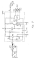
- FIG. 9 shows the structure of a complete transimpedance preamplifier, which contains the negative feedback amplifier stage with setting network NW at the output. It should be noted in FIG. 9 that the reference potential is interchanged with earlier images (FIG. 2). This preamplifier is driven directly by a photodiode, the equivalent circuit diagram of which is shown before input I of the preamplifier.
- the transimpedance is 750 ⁇ and the data rate is 6.5 Gbit / s.
- the capacitor C1 corresponds to the capacitor C1 of the example presented.
- the negative feedback via only one stage at the input by means of resistor R F leads to a frequency response characteristic with a higher bandwidth and fewer stability problems.
- caused by the single-stage negative feedback at high frequencies can be compensated by setting the network NW. 10 shows two examples with different increases in
- the phase chant of the amplifier can also be optimized in a simple manner by means of the network NW.
Landscapes
- Engineering & Computer Science (AREA)
- Power Engineering (AREA)
- Amplifiers (AREA)
- Optical Communication System (AREA)
Applications Claiming Priority (2)
| Application Number | Priority Date | Filing Date | Title |
|---|---|---|---|
| DE4204324 | 1992-02-14 | ||
| DE4204324 | 1992-02-14 |
Publications (2)
| Publication Number | Publication Date |
|---|---|
| EP0555748A1 true EP0555748A1 (fr) | 1993-08-18 |
| EP0555748B1 EP0555748B1 (fr) | 1998-05-13 |
Family
ID=6451641
Family Applications (1)
| Application Number | Title | Priority Date | Filing Date |
|---|---|---|---|
| EP93101630A Expired - Lifetime EP0555748B1 (fr) | 1992-02-14 | 1993-02-03 | Etage amplificateur à contre-réaction |
Country Status (3)
| Country | Link |
|---|---|
| EP (1) | EP0555748B1 (fr) |
| AT (1) | ATE166192T1 (fr) |
| DE (1) | DE59308517D1 (fr) |
Citations (2)
| Publication number | Priority date | Publication date | Assignee | Title |
|---|---|---|---|---|
| BE649319A (fr) * | 1963-07-11 | 1964-10-16 | ||
| EP0242439A2 (fr) * | 1986-04-23 | 1987-10-28 | Tektronix, Inc. | Amplificateur à large bande à compensation active haute fréquence |
-
1993
- 1993-02-03 AT AT93101630T patent/ATE166192T1/de not_active IP Right Cessation
- 1993-02-03 EP EP93101630A patent/EP0555748B1/fr not_active Expired - Lifetime
- 1993-02-03 DE DE59308517T patent/DE59308517D1/de not_active Expired - Fee Related
Patent Citations (2)
| Publication number | Priority date | Publication date | Assignee | Title |
|---|---|---|---|---|
| BE649319A (fr) * | 1963-07-11 | 1964-10-16 | ||
| EP0242439A2 (fr) * | 1986-04-23 | 1987-10-28 | Tektronix, Inc. | Amplificateur à large bande à compensation active haute fréquence |
Non-Patent Citations (2)
| Title |
|---|
| NACHRICHTEN TECHNIK ELEKTRONIK Bd. 35, Nr. 11, 1985, BERLIN DD Seiten 429 - 431 W. BAIER ET AL 'GEGENGEKOPPELTE DOPPELSTUFE IN OPTISCHEN EMPF[NGERN' * |
| RADIO FERNSEHEN ELEKTRONIK Bd. 26, Nr. 9, 1977, BERLIN DD Seite 316 'FELDST[RKEABH[NGIGE BANDBREITEN-REGELUNG IN AM-RUNDFUNKEMPF[NGERN' * |
Also Published As
| Publication number | Publication date |
|---|---|
| ATE166192T1 (de) | 1998-05-15 |
| EP0555748B1 (fr) | 1998-05-13 |
| DE59308517D1 (de) | 1998-06-18 |
Similar Documents
| Publication | Publication Date | Title |
|---|---|---|
| DE69219359T2 (de) | Transimpedanzverstärker | |
| DE3723778C2 (fr) | ||
| DE69603369T2 (de) | Begrenzender hochfrequenz-differenz-kettenverstärker | |
| DE102004043241B4 (de) | Transimpedanzverstärker mit veränderbarer Ausgangsamplitude und weitem Eingangsdynamikbereich | |
| DE69224677T2 (de) | Programmierbarer Verstärker | |
| DE69026720T2 (de) | Fiberoptischer Transimpedanz Empfänger | |
| DE1901804C3 (de) | Stabilisierter Differentialverstärker | |
| DE69424985T2 (de) | Transimpedanzverstärkerschaltung mit variablen Rückkopplungs- und Lastwiderstandsschaltungen | |
| DE69222161T2 (de) | System zur Abstimmung eines Qualitätsfaktors | |
| DE2950584C2 (de) | Schaltungsanordnung mit steuerbarem Widerstand | |
| DE69226862T2 (de) | Frequenzabstimmungssystem für ein Paar C-Transkonduktanzoperationsverstärker | |
| DE3420068C2 (fr) | ||
| DE19645417C2 (de) | Eingangsschutz für Verstärker mit großer Bandbreite | |
| DE69225589T2 (de) | Vorverstärker | |
| DE69717390T2 (de) | Eine niedrige Verzerrung mit grosser Amplitude enthaltende Abwärtsmischschaltung mit Filter und Verstärker | |
| DE2828697C2 (fr) | ||
| DE4433594C2 (de) | Biquad-Filter | |
| DE68920399T2 (de) | Filterschaltungsanordnung. | |
| DE2811626A1 (de) | Filter fuer digital-analog-wandler | |
| DE2438883B2 (de) | Durch rueckkopplung stabilisierte verstaerkeranordnung | |
| DE2836583C2 (fr) | ||
| DE69200132T2 (de) | Breitbandverstärkerstufe mit automatischer Verstärkungsregelung und Offsetregelung. | |
| DE1909721A1 (de) | Elektrische Schaltung zur Erzeugung von Vorspannungen | |
| DE2539586A1 (de) | Wechselspannungs-gleichspannungs- wandlersystem | |
| DE69120555T2 (de) | Breitband-Signalverstärker |
Legal Events
| Date | Code | Title | Description |
|---|---|---|---|
| PUAI | Public reference made under article 153(3) epc to a published international application that has entered the european phase |
Free format text: ORIGINAL CODE: 0009012 |
|
| 17P | Request for examination filed |
Effective date: 19930603 |
|
| AK | Designated contracting states |
Kind code of ref document: A1 Designated state(s): AT CH DE FR GB LI NL |
|
| 17Q | First examination report despatched |
Effective date: 19951109 |
|
| RAP1 | Party data changed (applicant data changed or rights of an application transferred) |
Owner name: ROBERT BOSCH GMBH |
|
| GRAG | Despatch of communication of intention to grant |
Free format text: ORIGINAL CODE: EPIDOS AGRA |
|
| GRAG | Despatch of communication of intention to grant |
Free format text: ORIGINAL CODE: EPIDOS AGRA |
|
| GRAH | Despatch of communication of intention to grant a patent |
Free format text: ORIGINAL CODE: EPIDOS IGRA |
|
| GRAH | Despatch of communication of intention to grant a patent |
Free format text: ORIGINAL CODE: EPIDOS IGRA |
|
| GRAA | (expected) grant |
Free format text: ORIGINAL CODE: 0009210 |
|
| AK | Designated contracting states |
Kind code of ref document: B1 Designated state(s): AT CH DE FR GB LI NL |
|
| REF | Corresponds to: |
Ref document number: 166192 Country of ref document: AT Date of ref document: 19980515 Kind code of ref document: T |
|
| REG | Reference to a national code |
Ref country code: CH Ref legal event code: EP |
|
| REF | Corresponds to: |
Ref document number: 59308517 Country of ref document: DE Date of ref document: 19980618 |
|
| GBT | Gb: translation of ep patent filed (gb section 77(6)(a)/1977) |
Effective date: 19980714 |
|
| ET | Fr: translation filed | ||
| PG25 | Lapsed in a contracting state [announced via postgrant information from national office to epo] |
Ref country code: GB Free format text: LAPSE BECAUSE OF NON-PAYMENT OF DUE FEES Effective date: 19990203 Ref country code: AT Free format text: LAPSE BECAUSE OF NON-PAYMENT OF DUE FEES Effective date: 19990203 |
|
| PG25 | Lapsed in a contracting state [announced via postgrant information from national office to epo] |
Ref country code: LI Free format text: LAPSE BECAUSE OF NON-PAYMENT OF DUE FEES Effective date: 19990228 Ref country code: CH Free format text: LAPSE BECAUSE OF NON-PAYMENT OF DUE FEES Effective date: 19990228 |
|
| PLBE | No opposition filed within time limit |
Free format text: ORIGINAL CODE: 0009261 |
|
| STAA | Information on the status of an ep patent application or granted ep patent |
Free format text: STATUS: NO OPPOSITION FILED WITHIN TIME LIMIT |
|
| 26N | No opposition filed | ||
| PG25 | Lapsed in a contracting state [announced via postgrant information from national office to epo] |
Ref country code: NL Free format text: LAPSE BECAUSE OF NON-PAYMENT OF DUE FEES Effective date: 19990901 |
|
| GBPC | Gb: european patent ceased through non-payment of renewal fee |
Effective date: 19990203 |
|
| REG | Reference to a national code |
Ref country code: CH Ref legal event code: PL |
|
| PG25 | Lapsed in a contracting state [announced via postgrant information from national office to epo] |
Ref country code: FR Free format text: LAPSE BECAUSE OF NON-PAYMENT OF DUE FEES Effective date: 19991029 |
|
| PG25 | Lapsed in a contracting state [announced via postgrant information from national office to epo] |
Ref country code: DE Free format text: LAPSE BECAUSE OF NON-PAYMENT OF DUE FEES Effective date: 19991201 |
|
| REG | Reference to a national code |
Ref country code: FR Ref legal event code: ST |