EP0556596B1 - Volldifferentieller spannungsgesteuerter Oszillator des Relaxationstyps und Verfahren zu dessen Betrieb - Google Patents
Volldifferentieller spannungsgesteuerter Oszillator des Relaxationstyps und Verfahren zu dessen Betrieb Download PDFInfo
- Publication number
- EP0556596B1 EP0556596B1 EP93101061A EP93101061A EP0556596B1 EP 0556596 B1 EP0556596 B1 EP 0556596B1 EP 93101061 A EP93101061 A EP 93101061A EP 93101061 A EP93101061 A EP 93101061A EP 0556596 B1 EP0556596 B1 EP 0556596B1
- Authority
- EP
- European Patent Office
- Prior art keywords
- terminal
- output
- capacitor
- transconductance amplifier
- coupled
- Prior art date
- Legal status (The legal status is an assumption and is not a legal conclusion. Google has not performed a legal analysis and makes no representation as to the accuracy of the status listed.)
- Expired - Lifetime
Links
- 238000000034 method Methods 0.000 title claims description 4
- 239000003990 capacitor Substances 0.000 claims description 53
- 230000005540 biological transmission Effects 0.000 claims description 37
- 230000008878 coupling Effects 0.000 claims description 4
- 238000010168 coupling process Methods 0.000 claims description 4
- 238000005859 coupling reaction Methods 0.000 claims description 4
- 230000007850 degeneration Effects 0.000 claims description 2
- 238000007599 discharging Methods 0.000 claims description 2
- 230000000295 complement effect Effects 0.000 description 9
- 238000010586 diagram Methods 0.000 description 8
- 239000013078 crystal Substances 0.000 description 7
- 208000037516 chromosome inversion disease Diseases 0.000 description 4
- 230000035945 sensitivity Effects 0.000 description 4
- 230000007423 decrease Effects 0.000 description 3
- 239000000758 substrate Substances 0.000 description 3
- 230000003292 diminished effect Effects 0.000 description 2
- 230000000694 effects Effects 0.000 description 2
- 238000005516 engineering process Methods 0.000 description 2
- 239000007787 solid Substances 0.000 description 2
- 238000004891 communication Methods 0.000 description 1
- 238000012986 modification Methods 0.000 description 1
- 230000004048 modification Effects 0.000 description 1
- 230000010355 oscillation Effects 0.000 description 1
- 238000012545 processing Methods 0.000 description 1
- 239000004065 semiconductor Substances 0.000 description 1
- 238000012546 transfer Methods 0.000 description 1
Images

Classifications
-
- H—ELECTRICITY
- H03—ELECTRONIC CIRCUITRY
- H03K—PULSE TECHNIQUE
- H03K3/00—Circuits for generating electric pulses; Monostable, bistable or multistable circuits
- H03K3/02—Generators characterised by the type of circuit or by the means used for producing pulses
- H03K3/023—Generators characterised by the type of circuit or by the means used for producing pulses by the use of differential amplifiers or comparators, with internal or external positive feedback
- H03K3/0231—Astable circuits
Definitions
- This invention relates generally to electrical circuits, and more particularly, to voltage controlled oscillators (VCOs).
- VCOs voltage controlled oscillators
- VCOs Voltage controlled oscillators
- PLLs phase locked loops
- a VCO receives an input voltage, and generates an output signal at a frequency proportional to the input voltage.
- VCOs are known in the art.
- One type is a crystal-controlled VCO.
- the crystal VCO includes an inverter connected across the terminals of a crystal.
- One capacitor has a first terminal connected to a first terminal of the crystal and another terminal connected to the input voltage.
- a second capacitor has a first terminal connected to a second terminal of the crystal and another terminal connected to a negative power supply voltage.
- a varactor is connected between the second terminal of the first capacitor and the negative power supply voltage.
- a ring oscillator has an odd number of inversion stages.
- the output of the last stage is connected to the input of the first stage. Oscillation occurs because a given logic state on the input of a first inversion stage propagates through an odd number of inversion stages.
- a signal inverted from the original input of the first stage eventually is presented to the input of the first stage.
- the output of the last stage thus oscillates at a frequency determined by the propagation delay through all the stages.
- a ring oscillator may be made into a VCO by making the delay proportional to the input voltage.
- each inverter stage includes a standard CMOS inverter.
- the ring oscillator VCO includes an additional transistor in the CMOS inverter.
- a P- or N-channel transistor is connected between the source of the transistor of the same conductivity type and the source-side supply. The input voltage is then applied to the gate of the additional transistor, thus controlling the switching speed.
- the relaxation oscillator relies on charging times of a capacitor to determine the frequency of the output signal. As the input voltage varies, the rate of charging of the capacitor similarly varies.
- the ring and relaxation oscillator VCOs are each susceptible to noise-induced jitter on the output signal.
- the crystal VCO requires both an external crystal and varactor, which are expensive in terms of both component cost and pin count. Thus, new VCO designs with intolerance to noise-induced jitter and low cost are needed.
- a fully-differential relaxation-type voltage controlled oscillator comprising a charging capacitor having first and second terminals, a comparator having first and second inputs respectively coupled to said first and second terminals of said charging capacitor, for providing third and fourth output signals in response thereto, said comparator having a predetermined hysteresis, means for latching said third and fourth output signals to provide said first and second output signals of the relaxation-type voltage controlled oscillator, and an operational transconductance amplifier for receiving an input voltage, characterised by: said operational transconductance amplifier providing first and second differential currents respectively to first and second output terminals in response thereto; and means for coupling either, said first output terminal of said operational transconductance amplifier to said first terminal of said charging capacitor and said second output terminal of said operational transconductance amplifier to said second terminal of said charging capacitor, or said first output terminal of said operational transconductance amplifier to said second terminal of said charging capacitor and said second output terminal of said operational transconductance amplifier to said first terminal of said
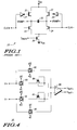
- FIG. 1 illustrates in partial schematic form and partial logic diagram form a relaxation-type voltage-controlled oscillator (VCO) core known in the prior art.
- VCO voltage-controlled oscillator
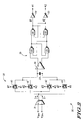
- FIG. 2 illustrates in partial schematic form and partial logic diagram form a preferred embodiment of a fully differential relaxation-type VCO in accordance with the present invention.
- FIG. 3 illustrates in partial schematic form and partial logic diagram form the operational transconductance amplifier of FIG. 2.
- FIG. 4 illustrates in partial schematic form and partial logic diagram form the comparator with hysteresis of FIG. 2.
- FIG. 1 illustrates in partial schematic form and partial logic diagram form a relaxation-type voltage-controlled oscillator (VCO) core 20 known in the prior art.
- VCO core 20 was disclosed by Wakayama and Abidi in "A 30-MHz Low-Jitter High Linearity CMOS Voltage Controlled Oscillator", IEEE Journal of Solid State Circuits , vol. SC-22, no. 6, December 1987, pp. 1074-1081.
- VCO core 20 includes NPN transistors 21 and 22, N-channel transistors 23 and 24, a capacitor 25, an N-channel transistor 26, and inverters 27 and 28.
- Transistors 21 and 22 each have a collector connected to a power supply voltage terminal labelled "V DD ", a base, and an emitter, the emitters of transistors 21 and 22 respectively providing signals labelled "VRAMP-" and "VRAMP+".
- V DD is a more-positive power supply voltage terminal typically at 5.0 volts.
- Transistor 23 has a drain connected to the emitter of transistor 21, a gate for receiving a clock signal labelled "CLK+”, and a source.
- Transistor 24 has drain connected to the emitter of transistor 22, a gate for receiving a clock signal labelled "CLK-”, and a source connected to the source of transistor 23.
- Capacitor 25 has a first terminal connected to the emitter of transistor 21, and a second terminal connected to the emitter of transistor 22.
- Transistor 26 has a drain connected to the sources of transistors 23 and 24, a gate for receiving a signal labelled "I BIAS ", and a source connected to a power supply voltage terminal labelled "V SS ".
- V SS is a more-negative power supply voltage terminal and is typically at zero volts.
- Inverter 27 has an input terminal for receiving signal CLK+, and an output terminal connected to the base of transistor 21.
- Inverter 28 has an input terminal for receiving signal CLK-, and an output terminal connected to the base of transistor 21.
- Signals CLK+ and CLK- are output signals of the VCO of which VCO core 20 is a part and are substantially complementary.
- I BIAS is a voltage which biases transistor 26 to conduct a current proportional to an input voltage (not shown).
- signal CLK+ is a logic high (and signal CLK- is a logic low)
- transistor 23 is conductive and transistor 24 is nonconductive.
- Inverter 28 provides a logic high voltage at the base of transistor 22, causing the second terminal of capacitor 25 to be at (V DD - V BE ), where V BE represents a forward-biased diode voltage drop.
- Transistors 23 and 26 decrease signal VRAMP- (the voltage at the first terminal of capacitor 25) at a rate determined by both the amount of current conducted through transistor 26 (which in turn depends on signal I BIAS ), and the value of capacitor 25. Since I BIAS is proportional to the input voltage, the rate at which capacitor 25 charges is determined by the input voltage.
- a differential dynamic latch (not shown) reverses the logic states of signals CLK+ and CLK-.
- a VCO based on VCO core 20 has a high sensitivity to power supply noise.
- the logic high voltages of inverters 27 and 28 are substantially at V DD , and the logic high voltages of VRAMP+ and VRAMP- are clamped at (V DD - V BE ).
- V DD - V BE the logic high voltages of VRAMP+ and VRAMP- are clamped at (V DD - V BE ).
- any noise on V DD affects the rate of charging of capacitor 25, and hence the period of signals CLK+ and CLK-.
- the gain of VCO core 20 is very high, and if the VCO is used in a PLL, any noise on the PLL's loop filter (not shown) is multiplied by the gain of VCO core 20.
- a new VCO with low jitter but also with low power supply sensitivity is needed.
- FIG. 2 illustrates in partial schematic form and partial logic diagram form a preferred embodiment of a fully differential relaxation-type VCO 30 in accordance with the present invention.
- VCO 30 includes generally an operational transconductance amplifier (OTA) 31, a selective switching portion 32, a capacitor 33, a comparator with hysteresis 34, and a latching portion 35.
- OTA operational transconductance amplifier
- Selective switching portion 32 includes transfer gates 40-44.
- Latching portion 35 includes NAND gates 50-53, and inverters 54 and 55.
- OTA 31 has a positive input terminal for receiving a signal labelled "V IN+ ", a negative input terminal for receiving a signal labelled "V IN- “, a positive output terminal for providing an output current signal labelled "I+”, and a negative output terminal for providing an output current signal labelled "I-"
- transmission gate 40 has a first terminal connected to the negative output terminal of OTA 31, a second terminal, a true control terminal for receiving signal F1, and a complement input terminal for receiving a signal labelled F1 ⁇ .
- Transmission gate 41 has a first terminal connected to the positive output terminal of OTA 31, a second terminal connected to the second terminal of transmission gate 40, a true control terminal for receiving signal F2, and a complement input terminal for receiving a signal labelled F2 ⁇ .
- Transmission gate 42 has a first terminal connected to the negative output terminal of OTA 31, a second terminal, a true control terminal for receiving signal F2, and a complement input terminal for receiving a signal labelled F2 ⁇ .
- Transmission gate 43 has a first terminal connected to the positive output terminal of OTA 31, a second terminal connected to the second terminal of transmission gate 42, a true control terminal for receiving signal F1, and a complement input terminal for receiving a signal labelled F1 ⁇ .
- Capacitor 33 has a first terminal connected to the second terminals of transmission gates 40 and 41, and a second terminal connected to the second terminals of transmission gates 42 and 43.
- Comparator 34 has a positive input terminal connected to the second terminals of transmission gates 40 and 41, a negative input terminal connected to the second terminals of transmission gates 42 and 43, a positive output terminal, and a negative output terminal.
- NAND gate 50 has a first input terminal connected to the positive output terminal of comparator 34, a second input terminal, and an output terminal.
- NAND gate 51 has a first input terminal connected to the output terminal of NAND gate 50, a second input terminal connected to the negative output terminal of comparator 34, and an output terminal connected to the second input terminal of NAND gate 50.
- NAND gate 52 has a first input terminal connected to the output terminal of NAND gate 50, a second input terminal, and an output terminal for providing signal F1 ⁇ .
- NAND gate 53 has a first input terminal connected to the output terminal of NAND gate 52, a second input terminal connected to the output terminal of NAND gate 51, and an output terminal connected to the second input terminal of NAND gate 52 and providing output signal F2 ⁇ thereon.
- Inverter 54 has an input terminal connected to the output terminal of NAND gate 52, and an output terminal for providing signal F1.
- Inverter 55 has an input terminal connected to the output terminal of NAND gate 53, and an output terminal for providing signal F2.
- OTA 31 receives a differential input voltage (between V IN+ and V IN- ) and provides differential current signals I+ and I- in response.
- signals F1 and F1 ⁇ are active at their respective logic states ("during F1")
- transmission gates 40 and 43 are active. Assuming V IN+ > V IN- , currents I+ and I- together provide positive charging between the second and first terminals of capacitor 33. Alternatively, if the first terminal of capacitor 33 is considered the positive terminal and the second terminal the negative terminal, then during F1, capacitor 33 is discharged.
- transmission gates 41 and 42 are active. Assuming V IN+ > V IN- , currents I+ and I- together provide positive charging between the first and second terminals of capacitor 33. Alternatively, during F2, capacitor 33 is charged. If, however, V IN+ ⁇ V IN- , then the periods of charging and discharging are reversed.
- comparator 34 detects a positive voltage between its positive and negative inputs, and provides a logic high voltage at the positive output terminal and a logic low voltage at the negative output terminal.
- NAND gates 50 and 51 form an SR flip flop, which is set in response to a logic high at the positive output terminal of comparator 34, and is reset in response to a logic high at the negative output terminal of comparator 34.
- NAND gates 52 and 53 function similarly and provide signals F1 ⁇ and F2 ⁇ in response. Signals F1 ⁇ and F2 ⁇ have approximately a fifty-percent duty cycle. After inversion by inverters 54 and 55, signals F1 and F2 also have a duty cycle of very nearly fifty percent.
- VCO 30 substantially decreases power supply voltage sensitivity.
- OTA 31 and comparator 34 are fully differential, and thus have high power-supply rejection ratio (PSRR) and common-mode rejection ratio (CMRR).
- PSRR power-supply rejection ratio
- CMRR common-mode rejection ratio
- OTA 31 charges capacitor 33 relative to its common-mode voltage, rather than relative to V DD or V SS . Since OTA 31 includes common-mode feedback, any noise on the common-mode voltage will be quickly compensated. Since the hysteresis of comparator 34 is approximately 0.8 volts, OTA 31 must only provide a 0.8-volt swing on capacitor 33.
- VCO 30 has a power supply sensitivity of less than 0.5%/volt and consumes only 25 milliwatts (mW) at 25 megahertz (MHz) operating frequency. It will be apparent to those skilled in the art, however, that this performance will vary somewhat with respect to different factors such as the designs of OTA 31 and comparator 34, and minimum gate length.
- FIG. 3 illustrates in partial schematic form and partial logic diagram form operational transconductance amplifier 31 of FIG. 2.
- OTA 31 includes P-channel transistors 60 and 61, N-channel transistors 62 and 63, P-channel transistors 64-67, a resistor 68, P-channel transistors 69 and 70, N-channel transistors 71 and 72, and a common-mode feedback block 75.
- Transistor 60 has a source connected to V DD , a gate for receiving a bias signal labelled "I BIAS ", and a drain.
- Transistor 61 has a source connected to the drain of transistor 60, a gate for receiving a bias voltage labelled "V1", and a drain for providing current I-.
- Transistor 62 has a drain connected to the drain of transistor 61, a gate for receiving a bias voltage labelled "V2", and a source.
- Transistor 63 has a drain connected to the source of transistor 62, a gate for receiving a signal labelled "V CMFB ", and a source connected to V SS .
- Transistor 64 has a source connected to V DD , a gate for receiving a bias signal labelled "I BIAS ", and a drain.
- Transistor 65 has a source connected to the drain of transistor 64, a gate for receiving signal V IN+ , and a drain connected to the drain of transistor 63.
- Transistor 66 has a source connected to V DD , a gate for receiving signal "I BIAS ", and a drain.
- Transistor 67 has a source connected to the drain of transistor 66, a gate for receiving signal V IN- , and a drain.
- Resistor 68 has a first terminal connected to the drain of transistor 64, and a second terminal connected to the drain of transistor 67.
- Transistor 69 has a source connected to V DD , a gate for receiving signal "I BIAS ", and a drain.
- Transistor 70 has a source connected to the drain of transistor 69, a gate for receiving bias voltage V2, and a drain for providing current I+.
- Transistor 71 has a drain connected to the drain of transistor 71, a gate for receiving bias voltage V2, and a source connected to the drain of transistor 67.
- Transistor 72 has a drain connected to the source of transistor 71, a gate for receiving signal V CMFB , and a source connected to V SS .
- Common-mode feedback block 75 has input terminals for receiving signals I+ and I-, and an output terminal for providing signal V CMFB .
- OTA 31 is a standard folded cascode operational amplifier with source degeneration.
- V1 and V2 are voltages sufficient to bias the transistors to which they are respectively applied into saturation.
- the differential voltage between V IN+ and V IN- results in differentially greater or lesser currents I+ and I-.
- Resistor 68 is added to linearize the output. For a large value of R, the transconductance is fixed and is approximately equal to (1/R).
- Common mode feedback block 75 senses the common mode voltage between the output nodes and alters signal V CMFB in response to a difference between the sensed common mode voltage and input reference voltage V REF .
- V REF is any desired reference voltage such as an analog ground reference voltage which is typically midway between V DD and V SS . It should be appreciated that other OTAs may also be used.
- FIG. 4 illustrates in partial schematic form and partial logic diagram form comparator with hysteresis 34 of FIG. 2.
- Comparator 34 includes transmission gates 80-83, P-channel transistors 84 and 85, and a comparator 86.
- Transmission gate 80 has a first terminal for receiving a voltage labelled "V+", a second terminal, a true control terminal for receiving signal F1, and a complement control terminal for receiving signal F1 ⁇ .
- the first terminal of transmission gate 80 forms the positive input terminal of comparator 34 and V+ is an input voltage corresponding to the voltages at the first terminal of capacitor 33 of FIG. 2.
- Transmission gate 81 has an first terminal for receiving a voltage labelled "V-", a second terminal, a true control terminal for receiving signal F2, and a complement control terminal for receiving signal F2 ⁇ .
- the first terminal of transmission gate 80 forms the negative input terminal of comparator 34 and V- is an input voltage corresponding to the voltages at the second terminal of capacitor 33 of FIG. 2.
- Transmission gate 82 has a first terminal for receiving signal V+, a second terminal, a true control terminal for receiving signal F2, and a complement input terminal for receiving a signal labelled F2 ⁇ .
- Transmission gate 83 has a first terminal for receiving signal V-, a second terminal, a true control terminal for receiving signal F1, and a complement input terminal for receiving a signal labelled F1 ⁇ .
- Transistor 84 has a source connected to the second terminal of transmission gate 80, a gate, and a bulk or substrate connected to a drain thereof.
- Transistor 85 has a source connected to the second terminal of transmission gate 81, a gate, and a bulk or substrate connected to a drain thereof.
- Comparator 86 has a positive input terminal connected to the second terminal of transmission gate 82 and to the drain of transistor 84, a negative input terminal connected to the second terminal of transmission gate 83 and to the drain of transistor 85, a positive output terminal for providing a signal labelled "V OUT+ ", and a negative output terminal for providing a signal labelled "V OUT- ".
- Signal V OUT+ is a voltage provided to the first input terminal of NAND gate 50 of FIG. 1
- signal V OUT- is a voltage provided to the second terminal of NAND gate 51 of FIG. 1.
- Comparator 34 provides a digital hysteresis and is more intolerant to variations in processing than other known designs.
- Comparator 86 is a conventional CMOS comparator which provides V OUT+ at a CMOS logic high voltage (approximately V DD ) and V OUT- at a CMOS logic low voltage (approximately V SS ) when the voltage at the positive input exceeds the voltage at the negative input thereof. Conversely, when the voltage at the negative input exceeds the voltage at the positive input thereof, V OUT+ is at a CMOS logic low and V OUT- is at a CMOS logic high.
- Transistors 84 and 85 provide a relatively-fixed voltage drop by having both their gates and their bulks tied to their respective drains. Thus, transistors 84 and 85 have a negative body effect or back bias, resulting in a diminished threshold voltage.
- transistors 84 and 85 each have gate widths of 80 microns and gate lengths of 4 microns, resulting in a threshold voltage of about 0.4 volts, compared to a threshold voltage of approximately 1.0 volts for a comparable P-channel transistor with a substrate connected to V DD .
- transmission gates 80 and 83 are conductive, and transmission gates 81 and 82 are nonconductive.
- Positive input voltage V+ is offset by the voltage drop through transistor 84; i.e., V+ must exceed V- by 0.4 volts for comparator 86 to switch.
- transmission gates 80 and 83 are nonconductive, and transmission gates 81 and 82 are conductive.
- Negative input voltage V- is offset by the voltage drop through transistor 85; i.e., V- must exceed V+ by 0.4 volts for comparator 86 to switch.
- comparator 34 provides a hysteresis of about 0.8 volts. This diminished hysteresis reduces the voltage swing required across capacitor 33 of FIG. 2.
Landscapes
- Manipulation Of Pulses (AREA)
- Inductance-Capacitance Distribution Constants And Capacitance-Resistance Oscillators (AREA)
- Stabilization Of Oscillater, Synchronisation, Frequency Synthesizers (AREA)
Claims (8)
- Ein volldifferentieller spannungsgesteuerter Oszillator (30) vom Relaxationstyp, umfassend eine Ladekapazität (33) mit einem ersten und einem zweiten Anschluß, einen Komparator (34) mit einem ersten und einem zweiten Eingang, die entsprechend an den ersten und den zweiten Anschluß der Ladekapazität (33) gekoppelt sind, um als Antwort darauf ein drittes und ein viertes Ausgangssignal zu schaffen, wobei der Komperator (34) eine vorbestimmte Hysterese hat, eine Einrichtung (35) zum Latchen des dritten und vierten Ausgangssignals, um das erste und das zweite Ausgangssignal des spannungsgesteuerten Oszillators (30) vom Relaxationstyp zu schaffen, und einen Transkonduktanzverstärker (31) zum Aufnehmen einer Eingangsspannung, gekennzeichnet durch:einen Transkonduktanzverstärker (31), der als Antwort einen ersten und einen zweiten differentiellen Strom entsprechend an den ersten und den zweiten Ausgangsanschluß liefert; undeine Einrichtung (32) zum selektiven Koppeln, als Antwort auf das erste und das zweite Ausgangssignal des spannungsgesteuerten Oszillators (30) vom Relaxationstyp, von entweder dem ersten Ausgangsanschluß des Transkonduktanzverstärkers (31) mit dem ersten Anschluß der Ladekapazität (33) und dem zweiten Ausgangsanschluß des Transkonduktanzverstärkers (31) mit dem zweiten Anschluß der Ladekapazität (33), oder dem ersten Ausgangsanschluß des Transkonduktanzverstärkers (31) mit dem zweiten Anschluß der Ladekapazität (33) und dem zweiten Ausgangsanschluß des Transkonduktanzverstärkers (31) mit dem ersten Anschluß der Ladekapazität (33).
- Der spannungsgesteuerte Oszillator (30) nach Anspruch 1, in welchem der Transkonduktanzverstärker (31) die Eingangsspannung zwischen den positiven und negativen Eingangsanschlüssen desselben empfängt.
- Der spannungsgesteuerte Oszillator (30) nach Anspruch 1, in welchem der Transkonduktanzverstärker (31) dadurch gekennzeichnet ist, daß er ein gefalteter Kaskoden-Transkonduktanzverstärker mit Quellendegenerierung ist.
- Der spannungsgesteuerte Osziallator (30) nach Anspruch 1, in welchem der Transkonduktanzverstärker (31) eine Einrichtung (75) zum Einstellen einer Gleichtaktspannung desselben umfaßt.
- Der spannungsgesteuerte Oszillator (30) nach Anspruch 1, in welchem die Einrichtung (32) zum Koppeln umfaßt:ein erstes Transfergatter (41), das einen ersten Anschluß, der mit dem positiven Ausgangsanschluß des Transkonduktanzverstärkers (31) gekoppelt ist, und einen zweiten Anschluß, der mit dem ersten Anschluß der Kapazität (33) gekoppelt ist, aufweist und als Antwort auf das zweite Ausgangssignal des Oszillators (30) aktiviert wird; undein zweites Transfergatter (42), das einen ersten Anschluß, der an den negativen Ausgangsanschluß des Transkonduktanzverstärkers (31) gekoppelt ist, und einen zweiten Anschluß, der an den zweiten Anschluß der Kapazität (33) gekoppelt ist, aufweist und als Antwort auf das zweite Ausgangssignal des Oszillators (30) aktiviert wird.
- Der spannungsgesteuerte Oszillator (30) nach Anspruch 5, in welchem die Einrichtung (32) zum Koppeln weiter aufweist:ein drittes Transfergatter (40), das einen ersten Anschluß, der an den negativen Ausgangsanschluß des Transkonduktanzverstärkers (31) gekoppelt ist, und einen zweiten Anschluß, der an den ersten Anschluß der Kapazität (33) gekoppelt ist, aufweist und als Antwort auf das erste Ausgangssignal des Oszillators (30) aktiviert wird; undein viertes Transfergatter (43), das einen ersten Anschluß, der an den positiven Ausgangsanschluß des Transkonduktanzverstärkers (31) gekoppelt ist, und einen zweiten Anschluß, der an den zweiten Anschluß der Kapazität (33) gekoppelt ist, aufweist und als Antwort auf das erste Ausgangssignal des Oszillators (30) aktiviert wird.
- Der spannungsgesteuerte Oszillator (30) nach Anspruch 1, in welchem der Komparator (34) aufweist:ein erstes Transfergatter (80), das einen ersten Anschluß, der an den ersten Anschluß der Ladekapazität (33) gekoppelt ist, sowie einen zweiten Anschluß aufweist und als Antwort auf das erste Ausgangssignal operativ ist;ein zweites Transfergatter (81), das einen ersten Anschluß, der an den zweiten Anschluß der Ladekapazität (33) gekoppelt ist, sowie einen zweiten Anschluß aufweist und als Antwort auf das zweite Ausgangssignal operativ ist;ein drittes Transfergatter (82), das einen ersten Anschluß, der an den ersten Anschluß der Ladekapazität (33) gekoppelt ist, sowie einen zweiten Anschluß aufweist und als Antwort auf das zweite Ausgangssignal operativ ist;ein viertes Transfergatter (83), das einen ersten Anschluß, der an den zweiten Anschluß der Ladekapazität (33) gekoppelt ist, sowie einen zweiten Anschluß aufweist und als Antwort auf das erste Ausgangssignal operativ ist;einen ersten P-Kanal-Transistor (84) mit einer Quelle, die an den zweiten Anschluß des ersten Transfergatters (80) gekoppelt ist, einem Gate, einer Senke, die an das Gate gekoppelt ist, und einem Volumen, das an die Senke gekoppelt ist;einen zweiten P-Kanal-Transistor (85) mit einer Quelle, die an den zweiten Anschluß des zweiten Transfergatters (81) gekoppelt ist, einem Gate, einer Senke, die an das Gate gekoppelt ist, und einem Volumen, das an die Senke gekoppelt ist; undeine Komparatorschaltung (86) mit einem positiven Eingangsanschluß, der an die Senke des ersten P-Kanal-Transistors (84) gekoppelt ist, einem negativen Eingangsanschluß, der an die Senke des zweiten P-Kanal-Transistors (85) gekoppelt ist, einem positiven Ausgangsanschluß zur Lieferung des dritten Ausgangssignals und einem negativen Ausgangsanschluß zur Lieferung des vierten Ausgangssignals.
- Ein Verfahren zum Schaffen eines ersten und eines zweiten Ausgangssignals mit einer Frequenz, die proportional zu einer Eingangsspannung ist, wobei das erste und das zweite Ausgangssignal entgegengesetzte Phasen haben, umfassend die Schritte des Schaffens des ersten Ausgangssignals mit einem logischen Hochpegel und des zweiten Ausgangssignals mit einem logischen Tiefpegel als Antwort auf eine Spannung zwischen einem ersten Anschluß einer Kapazität (33) und einem zweiten Anschluß der Kapazität (33), welche einen ersten vorbestimmten Wert übersteigt, des Schaffens des ersten Ausgangssignals mit einem logischen Tiefpegel und des zweiten Ausgangssignals mit einem logischen Hochpegel als Antwort auf eine Spannung zwischen dem zweiten Anschluß der Kapazität (33) und dem ersten Anschluß der Kapazität (33), welche einen zweiten vorbestimmten Wert übersteigt, und des Aufnehmens einer Eingangsspannung an dem Eingang eines Transkonduktanzverstärkers (31), dadurch gekennzeichnet, daß das Verfahren weiter die Schritte aufweist:Laden der Kapazität (33) mit der Ausgabe eines differentiellen Stromsignals des Transkonduktanzverstärkers (31) als Antwort auf das erste Ausgangssignal; undEntladen der Kapazität (33) mit der Ausgabe eines differentiellen Stromsignals des Transkonduktanzverstärkers (31) als Antwort auf das zweite Ausgangssignal.
Applications Claiming Priority (2)
| Application Number | Priority Date | Filing Date | Title |
|---|---|---|---|
| US835835 | 1992-02-18 | ||
| US07/835,835 US5194831A (en) | 1992-02-18 | 1992-02-18 | Fully-differential relaxation-type voltage controlled oscillator and method therefor |
Publications (2)
| Publication Number | Publication Date |
|---|---|
| EP0556596A1 EP0556596A1 (de) | 1993-08-25 |
| EP0556596B1 true EP0556596B1 (de) | 1997-04-09 |
Family
ID=25270595
Family Applications (1)
| Application Number | Title | Priority Date | Filing Date |
|---|---|---|---|
| EP93101061A Expired - Lifetime EP0556596B1 (de) | 1992-02-18 | 1993-01-25 | Volldifferentieller spannungsgesteuerter Oszillator des Relaxationstyps und Verfahren zu dessen Betrieb |
Country Status (4)
| Country | Link |
|---|---|
| US (1) | US5194831A (de) |
| EP (1) | EP0556596B1 (de) |
| JP (1) | JPH0645878A (de) |
| DE (1) | DE69309519T2 (de) |
Families Citing this family (18)
| Publication number | Priority date | Publication date | Assignee | Title |
|---|---|---|---|---|
| US5426384A (en) * | 1993-12-27 | 1995-06-20 | Motorola, Inc. | Voltage controlled oscillator (VCO) with symmetrical output and logic gate for use in same |
| US5428318A (en) * | 1994-02-15 | 1995-06-27 | At&T Corp. | Voltage controlled ring oscillator producing a sum output |
| US5559892A (en) * | 1994-03-28 | 1996-09-24 | Knowles Electronics, Inc. | Impedence buffering MOS circuit with dynamically reduced threshold voltage, as for use in an output buffer of a hearing aid amplifier |
| US5446413A (en) * | 1994-05-20 | 1995-08-29 | Knowles Electronics, Inc. | Impedance circuit for a miniature hearing aid |
| JP3023591B2 (ja) * | 1995-01-25 | 2000-03-21 | 日本プレシジョン・サーキッツ株式会社 | 電圧制御発振回路 |
| US6278336B1 (en) * | 1998-02-27 | 2001-08-21 | Texas Instruments Incorporated | Low-current oscillator with hysteresis input buffer |
| JP3753925B2 (ja) * | 2000-05-12 | 2006-03-08 | 株式会社ルネサステクノロジ | 半導体集積回路 |
| US6686806B2 (en) | 2000-12-14 | 2004-02-03 | Tropian, Inc. | Ring VCO based on RC timing |
| TW541788B (en) * | 2002-06-19 | 2003-07-11 | Ind Tech Res Inst | The frequency-tuning loop used in the transconductor-capacitor filter |
| KR100440634B1 (ko) * | 2002-09-09 | 2004-07-19 | 한국전자통신연구원 | 연속시간 필터의 자동튜닝장치 |
| KR100445998B1 (ko) * | 2002-09-30 | 2004-08-25 | 인티그런트 테크놀로지즈(주) | 트랜스컨덕터-커패시터 필터의 디지털 튜닝 회로 |
| JP2004297631A (ja) * | 2003-03-28 | 2004-10-21 | Nec Electronics Corp | コモンモード電圧制御回路及びコモンモード電圧制御方法 |
| US7663442B2 (en) * | 2005-03-28 | 2010-02-16 | Intel Corporation | Data receiver including a transconductance amplifier |
| US8373502B1 (en) * | 2011-09-20 | 2013-02-12 | Hong Kong Applied Science and Technology Research Institute Company Limited | Gm-C filter tuning circuit based on relaxation oscillator |
| CN103312298B (zh) * | 2013-07-05 | 2015-07-29 | 东南大学 | 一种提高频率-控制电流线性度的张弛振荡器 |
| US10181840B1 (en) * | 2014-08-21 | 2019-01-15 | National Technology & Engineering Solutions Of Sandia, Llc | Gm-C filter and multi-phase clock circuit |
| CN108092502B (zh) * | 2017-12-27 | 2019-11-22 | 西安电子科技大学 | 双模式宽负载范围降压型开关电容dc-dc转换器 |
| CN113839649B (zh) * | 2021-09-16 | 2023-11-21 | 英韧科技(上海)有限公司 | 张弛振荡器、集成电路和电子设备 |
Citations (1)
| Publication number | Priority date | Publication date | Assignee | Title |
|---|---|---|---|---|
| EP0401552A2 (de) * | 1989-06-05 | 1990-12-12 | Motorola, Inc. | Differentialer Kipposzillator |
Family Cites Families (1)
| Publication number | Priority date | Publication date | Assignee | Title |
|---|---|---|---|---|
| JPS62260420A (ja) * | 1986-04-28 | 1987-11-12 | シ−メンス、アクチエンゲゼルシヤフト | 集積nmos回路装置 |
-
1992
- 1992-02-18 US US07/835,835 patent/US5194831A/en not_active Expired - Lifetime
-
1993
- 1993-01-25 EP EP93101061A patent/EP0556596B1/de not_active Expired - Lifetime
- 1993-01-25 DE DE69309519T patent/DE69309519T2/de not_active Expired - Fee Related
- 1993-02-12 JP JP5046120A patent/JPH0645878A/ja active Pending
Patent Citations (1)
| Publication number | Priority date | Publication date | Assignee | Title |
|---|---|---|---|---|
| EP0401552A2 (de) * | 1989-06-05 | 1990-12-12 | Motorola, Inc. | Differentialer Kipposzillator |
Also Published As
| Publication number | Publication date |
|---|---|
| DE69309519D1 (de) | 1997-05-15 |
| US5194831A (en) | 1993-03-16 |
| JPH0645878A (ja) | 1994-02-18 |
| EP0556596A1 (de) | 1993-08-25 |
| DE69309519T2 (de) | 1997-11-13 |
Similar Documents
| Publication | Publication Date | Title |
|---|---|---|
| US5194831A (en) | Fully-differential relaxation-type voltage controlled oscillator and method therefor | |
| US6084452A (en) | Clock duty cycle control technique | |
| US6385265B1 (en) | Differential charge pump | |
| US5426384A (en) | Voltage controlled oscillator (VCO) with symmetrical output and logic gate for use in same | |
| US5621340A (en) | Differential comparator for amplifying small swing signals to a full swing output | |
| US7298183B2 (en) | High frequency divider circuits and methods | |
| US5565817A (en) | Ring oscillator having accelerated charging and discharging of capacitors | |
| US7102342B2 (en) | Current reference circuit with voltage-to-current converter having auto-tuning function | |
| US6469585B1 (en) | Low phase noise ring-type voltage controlled oscillator | |
| US5469116A (en) | Clock generator circuit with low current frequency divider | |
| US5298870A (en) | Voltage controlled ring oscillator having differential amplifier stages | |
| JPH06104638A (ja) | 電流/電圧制御される高速オッシレータ回路 | |
| US6075419A (en) | High speed wide tuning range multi-phase output ring oscillator | |
| US5585764A (en) | High-speed voltage controlled oscillator which is insensitive to changes in power supply voltage | |
| US20020190798A1 (en) | Ring oscillator circuit and a delay circuit | |
| US5714912A (en) | VCO supply voltage regulator | |
| EP0361529B1 (de) | Spannungsgesteuerter Oszillator | |
| US5880579A (en) | VCO supply voltage regulator for PLL | |
| EP0771491B1 (de) | Phazenregelkreis mit einem grossen frequenzbereich und sehr niedrigem rauschen | |
| US6278334B1 (en) | Voltage controlled oscillator with accelerating and decelerating circuits | |
| US4383224A (en) | NMOS Crystal oscillator | |
| US7511584B2 (en) | Voltage controlled oscillator capable of operating in a wide frequency range | |
| JPH0856158A (ja) | 電圧制御発振器 | |
| JPH07202646A (ja) | 電圧制御発振回路 | |
| KR980012888A (ko) | 공통모드 발진 및 입력 히스테리시스를 방지하는 차동 지연 소자 |
Legal Events
| Date | Code | Title | Description |
|---|---|---|---|
| PUAI | Public reference made under article 153(3) epc to a published international application that has entered the european phase |
Free format text: ORIGINAL CODE: 0009012 |
|
| AK | Designated contracting states |
Kind code of ref document: A1 Designated state(s): DE FR GB IT |
|
| 17P | Request for examination filed |
Effective date: 19940210 |
|
| 17Q | First examination report despatched |
Effective date: 19950505 |
|
| GRAG | Despatch of communication of intention to grant |
Free format text: ORIGINAL CODE: EPIDOS AGRA |
|
| GRAH | Despatch of communication of intention to grant a patent |
Free format text: ORIGINAL CODE: EPIDOS IGRA |
|
| GRAH | Despatch of communication of intention to grant a patent |
Free format text: ORIGINAL CODE: EPIDOS IGRA |
|
| ITF | It: translation for a ep patent filed | ||
| GRAA | (expected) grant |
Free format text: ORIGINAL CODE: 0009210 |
|
| AK | Designated contracting states |
Kind code of ref document: B1 Designated state(s): DE FR GB IT |
|
| REF | Corresponds to: |
Ref document number: 69309519 Country of ref document: DE Date of ref document: 19970515 |
|
| ET | Fr: translation filed | ||
| PGFP | Annual fee paid to national office [announced via postgrant information from national office to epo] |
Ref country code: GB Payment date: 19971229 Year of fee payment: 6 |
|
| PGFP | Annual fee paid to national office [announced via postgrant information from national office to epo] |
Ref country code: FR Payment date: 19980116 Year of fee payment: 6 |
|
| PGFP | Annual fee paid to national office [announced via postgrant information from national office to epo] |
Ref country code: DE Payment date: 19980120 Year of fee payment: 6 |
|
| PLBE | No opposition filed within time limit |
Free format text: ORIGINAL CODE: 0009261 |
|
| STAA | Information on the status of an ep patent application or granted ep patent |
Free format text: STATUS: NO OPPOSITION FILED WITHIN TIME LIMIT |
|
| 26N | No opposition filed | ||
| PG25 | Lapsed in a contracting state [announced via postgrant information from national office to epo] |
Ref country code: GB Free format text: LAPSE BECAUSE OF NON-PAYMENT OF DUE FEES Effective date: 19990125 |
|
| GBPC | Gb: european patent ceased through non-payment of renewal fee |
Effective date: 19990125 |
|
| PG25 | Lapsed in a contracting state [announced via postgrant information from national office to epo] |
Ref country code: FR Free format text: LAPSE BECAUSE OF NON-PAYMENT OF DUE FEES Effective date: 19990930 |
|
| PG25 | Lapsed in a contracting state [announced via postgrant information from national office to epo] |
Ref country code: DE Free format text: LAPSE BECAUSE OF NON-PAYMENT OF DUE FEES Effective date: 19991103 |
|
| REG | Reference to a national code |
Ref country code: FR Ref legal event code: ST |
|
| PG25 | Lapsed in a contracting state [announced via postgrant information from national office to epo] |
Ref country code: IT Free format text: LAPSE BECAUSE OF NON-PAYMENT OF DUE FEES Effective date: 20050125 |