EP0557910A2 - Commutateur de cellules - Google Patents
Commutateur de cellules Download PDFInfo
- Publication number
- EP0557910A2 EP0557910A2 EP93102689A EP93102689A EP0557910A2 EP 0557910 A2 EP0557910 A2 EP 0557910A2 EP 93102689 A EP93102689 A EP 93102689A EP 93102689 A EP93102689 A EP 93102689A EP 0557910 A2 EP0557910 A2 EP 0557910A2
- Authority
- EP
- European Patent Office
- Prior art keywords
- output
- cell
- switch
- cells
- group
- Prior art date
- Legal status (The legal status is an assumption and is not a legal conclusion. Google has not performed a legal analysis and makes no representation as to the accuracy of the status listed.)
- Granted
Links
Images


Classifications
-
- H—ELECTRICITY
- H04—ELECTRIC COMMUNICATION TECHNIQUE
- H04L—TRANSMISSION OF DIGITAL INFORMATION, e.g. TELEGRAPHIC COMMUNICATION
- H04L12/00—Data switching networks
- H04L12/54—Store-and-forward switching systems
- H04L12/56—Packet switching systems
- H04L12/5601—Transfer mode dependent, e.g. ATM
-
- H—ELECTRICITY
- H04—ELECTRIC COMMUNICATION TECHNIQUE
- H04L—TRANSMISSION OF DIGITAL INFORMATION, e.g. TELEGRAPHIC COMMUNICATION
- H04L49/00—Packet switching elements
- H04L49/10—Packet switching elements characterised by the switching fabric construction
- H04L49/104—Asynchronous transfer mode [ATM] switching fabrics
- H04L49/105—ATM switching elements
- H04L49/106—ATM switching elements using space switching, e.g. crossbar or matrix
-
- H—ELECTRICITY
- H04—ELECTRIC COMMUNICATION TECHNIQUE
- H04L—TRANSMISSION OF DIGITAL INFORMATION, e.g. TELEGRAPHIC COMMUNICATION
- H04L49/00—Packet switching elements
- H04L49/15—Interconnection of switching modules
- H04L49/1515—Non-blocking multistage, e.g. Clos
- H04L49/153—ATM switching fabrics having parallel switch planes
-
- H—ELECTRICITY
- H04—ELECTRIC COMMUNICATION TECHNIQUE
- H04L—TRANSMISSION OF DIGITAL INFORMATION, e.g. TELEGRAPHIC COMMUNICATION
- H04L49/00—Packet switching elements
- H04L49/40—Constructional details, e.g. power supply, mechanical construction or backplane
- H04L49/405—Physical details, e.g. power supply, mechanical construction or backplane of ATM switches
-
- H—ELECTRICITY
- H04—ELECTRIC COMMUNICATION TECHNIQUE
- H04Q—SELECTING
- H04Q11/00—Selecting arrangements for multiplex systems
- H04Q11/04—Selecting arrangements for multiplex systems for time-division multiplexing
- H04Q11/0428—Integrated services digital network, i.e. systems for transmission of different types of digitised signals, e.g. speech, data, telecentral, television signals
- H04Q11/0478—Provisions for broadband connections
-
- H—ELECTRICITY
- H04—ELECTRIC COMMUNICATION TECHNIQUE
- H04L—TRANSMISSION OF DIGITAL INFORMATION, e.g. TELEGRAPHIC COMMUNICATION
- H04L12/00—Data switching networks
- H04L12/54—Store-and-forward switching systems
- H04L12/56—Packet switching systems
- H04L12/5601—Transfer mode dependent, e.g. ATM
- H04L2012/5625—Operations, administration and maintenance [OAM]
- H04L2012/5627—Fault tolerance and recovery
-
- H—ELECTRICITY
- H04—ELECTRIC COMMUNICATION TECHNIQUE
- H04L—TRANSMISSION OF DIGITAL INFORMATION, e.g. TELEGRAPHIC COMMUNICATION
- H04L12/00—Data switching networks
- H04L12/54—Store-and-forward switching systems
- H04L12/56—Packet switching systems
- H04L12/5601—Transfer mode dependent, e.g. ATM
- H04L2012/5638—Services, e.g. multimedia, GOS, QOS
- H04L2012/5646—Cell characteristics, e.g. loss, delay, jitter, sequence integrity
- H04L2012/565—Sequence integrity
-
- H—ELECTRICITY
- H04—ELECTRIC COMMUNICATION TECHNIQUE
- H04L—TRANSMISSION OF DIGITAL INFORMATION, e.g. TELEGRAPHIC COMMUNICATION
- H04L12/00—Data switching networks
- H04L12/54—Store-and-forward switching systems
- H04L12/56—Packet switching systems
- H04L12/5601—Transfer mode dependent, e.g. ATM
- H04L2012/5678—Traffic aspects, e.g. arbitration, load balancing, smoothing, buffer management
- H04L2012/5681—Buffer or queue management
Definitions
- the present invention relates generally to asynchronous transfer mode (ATM) networks and more particularly to a cell exchanging system for relaying cells and exchanging cells at a high speed.
- ATM asynchronous transfer mode
- ATM techniques have been proposed to switch voice data, video data, and other kinds of data.
- the ATM techniques are designed for use in a digital network such as an integrated services digital network (ISDN).
- ISDN integrated services digital network
- ATM techniques improve the utilization efficiency of transmission in switching by statistical multiplexing of fixed length packets of the data, known as cells, on a broad band transmission line.
- the architectures for practicing ATM techniques include switching architectures for switching cells through the network.
- Fig. 11 is a block diagram showing the change- over system of an ATM switch, which is described in Japanese Patent Lain-Open No. Hei 3-26038.
- the ATM switch is used to direct cells through the ATM network.
- this ATM switch is provided with two ATM switch systems #1 and #2, which have the same structure. Redundant switch systems are provided to enhance the robustness of the network.
- ATM buffer cell counters 31 a and 31 are provided in order to monitor the number of cells which are stored in the ATM switch buffers 30a and 30b. Each of the ATM buffer cell counters 31 a and 32b increments its count value each time an ATM cell is input to the corresponding ATM switch buffer 30a and 30b, and decrements its count value each time an ATM cell is output from the corresponding buffer. In this way, the ATM buffer cell counters 31 a and 31 b always monitor the number of cells that are stored in the respective ATM switch buffers 30a and 30b.
- Systems #1 and #2 are provided with respective difference detectors 33a and 33b, for comparing the count values of the ATM buffer cell counters 31 a and 31 b.
- Systems #1 and #2 are also provided with respective dummy cell markers 32a and 32b for writing dummy cells into the ATM switch buffers 30a and 30b, in accordance with the control signals sent from the difference detectors 33a and 33b.
- a plurality of ATM switches are disposed at intersections (cross points) of input and output paths so as to form a crossbar type ATM exchanging apparatus.
- each of the ATM switch buffers 30a and 30b stores the same cells "1 "-"2", as shown in Fig. 12A. Accordingly, each of the ATM buffer cell counters 31 a and 31 b has a counter value of "4".
- difference detector 33b detects the difference between the count values of the ATM buffer cell counters 31 a and 31 b.
- Difference detector 33b causes the dummy cell marker 32b to generate dummy cells (indicated by "0" entries) which are stored in the ATM switch buffer 30b until the difference in count values is eliminated. Dummy cells are, thus, stored until there is no difference between the count values of the ATM buffer cell counters 31 a an 31b, and hence the number of cells stored in the ATM switch buffer 30a equals the number of cells stored in the ATM switch buffer 30b.
- switch system #2 begins to operate in the same way as switch system #1.
- Fig. 13A shows a subsequent state in which the leading four cells in buffers 30a and 30b have been output and in which four new cells have been supplied to the ATM switch buffers.
- Fig. 13B shows the state in which two additional cells (six cells in total) have been supplied to the ATM switch buffers 30a and 30b and the leading three cells have been removed from the buffers 30a and 30b.
- switch system #2 cannot function as a "spare" system. In other words, switch system #2 cannot be called upon to assume the role previously served by switch system #1.
- switch system #2 can be changed over to assume the role of system #1.
- one control unit is shared by two switch systems so as to control which of a plurality of ATM systems for outputting cells to the same output path should output a cell.
- the status of cells stored in the switch buffers are the same for the two switch systems.
- the control units cannot be doubled.
- an object of the present invention to provide a cell exchanging apparatus which comprises two independent ATM switch systems and can perform change-over of the switches without duplication of cells and omission of the cells, and to provide a method therefor.
- an asynchronous transfer mode (ATM) cell exchanging apparatus distributes input cells to corresponding cell output lines.
- Each input cell includes a data portion and a header portion.
- the header portion includes address information that is used to direct the cell to its destination.
- the cell exchanging apparatus includes a first cell switch for distributing the input cells to a first set of switch output lines in accordance with address information of the header portions of the input cells.
- the cell exchanging apparatus also includes a second redundant cell switch for distributing the input cells to a second set of switch output lines in accordance with address information of the header portions of the input cells. Both the first and second cell switches generate idle cells when they input cells.
- the cell exchanging apparatus further includes a selection mechanism for determining which of the first and second sets of switch output lines is a currently selected switch of output lines that provides cells to the cell output lines.
- the selection mechanism is switchable between selecting the first set of switch output lines and the second set of switch output lines.
- the selection mechanism includes a confirmation mechanism for confirming that idle cells are output on each of the currently selected and spare sets of switch output lines before switching selection by the selection mechanism of cells from the currently selected set of switch output lines to the other set of switch output lines.
- the first cell switch and/or the second cell switch may be formed by a plurality of unit switches.
- the first and second cell switches may include arbitration logic for arbitrating competing requests to output a cell over a switch output line.
- each of the unit switches is provided with an output buffer that temporarily stores the cells to the output.
- the unit switches request permission to output a cell when a cell is stored in its output buffer.
- the arbitration circuit grants permission to one of the unit switches which are connected to a single switch output line and which are requesting permission to output a cell so that only the cell in the unit switch which is granted permission is output to the switch output line.
- the arbitration circuit instructs one of the unit switches to output an idle cell when no unit switch requests permission to output a cell.
- a cell exchanging apparatus which comprises a first cell switch which distributes cells input through input lines by destinations and a second cell switch which has the same configuration as the first cell switch; one cell switch operates as an active system and the other operates as a standby system.
- Cells input to the cell exchanging apparatus are fed through input selectors only to the cell switch operating as the active system, and output selectors output cells output from the cell switch as the active system to an external system as output of the cell exchanging apparatus.
- the cell switch in the standby mode changes to a new active cell switch which then starts to send cells to the output selectors.
- the cell switches as the active and standby systems can be changed over.
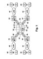
- Fig. 1 shows a digital transmission system in which the cell exchanging apparatus of the present invention may be used.
- the digital transmission system of Fig. 1 includes an ATM communication network 50.
- the system also includes terminals 40 that serve as the source and destination of cells that are passed across the network.
- the terminals are connected to local area networks (LANs) 42, which are, in turn, connected to cell multiplexing devices 44.
- LANs local area networks
- the cell multiplexing devices 44 serve as interfaces between LANs 42 and the ATM communication network 50.
- Cells originating from a terminal pass through a LAN 42 to a cell multiplexing device 44, wherein the cells are multiplexed across the ATM communication network 50.
- Each of the cell multiplexing devices 44 is connected to a number of logical channels 46.
- the cell multiplexer decides which channel the cells are transmitted across. In making this decision, the cell multiplexing device selects a particular channel 52 that leads to the destination terminal.
- the cells are demultiplexed by a cell multiplexer device 44 that is coupled to a LAN 42 leading to the destination terminal 40. The demultiplexed cells are then transmitted over the LAN 42 to the destination terminal 40.
- the ATM communication network 50 must include a number of switches to properly route cells across the network.
- the ATM network 50 is designed to operate at very high speeds (e.g., line bit-rates of 155 Mbps). As such, the switching must be done efficiently to maintain a high throughput.
- the present invention provides a cell exchanging apparatus that performs switching without omitting cells or repeating cells.
- a first preferred embodiment of a cell exchanging apparatus is shown in Fig. 2.
- the ATM cell exchanging apparatus of Fig. 2 is provided with a cell switch 11 for receiving cells from a plurality of input lines 2a to 2n (where n is a positive integer) and for outputting the received cells to a plurality of output lines 3a to 3n (where n is a positive integer).
- the ATM cell switching apparatus also includes an additional cell switch 12 that serves as a "spare cell” switch.
- This cell switch 12 has the same structure as cell switch 11 but has separate output lines 4a to 4m.
- Selectors 5a to 5m are coupled to the output lines 3a-3m and 4a-4m of the respective switches 11 and 12.
- the selectors 5a-5m select either the output lines 3a to 3m of cell switch 11 or the output lines 4a to 4m of cell switch 12.
- the selectors 5a to 5m output cells received from the selected lines through lines 6a to 6m.
- the selectors 5a to 5m make their choice of lines based on the system change-over signal. This signal will be described in more detail below.
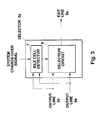
- Fig. 3 is a block diagram of the structure of selector 5a. Each of the other selectors 5b-5m has an identical construction.
- the selector 5a includes an idle cell detector 7, for judging whether or not an idle or idle cell is output on the output lines 3a and 4a.
- the cell switch 11 or 12 (Fig. 1) has no cell to output to one of its output lines, an idle cell is output in place of a normal cell.
- Each cell is typically 53 bytes in length, with 48 bytes of data and 5 bytes of header information.
- the cell switch 11 or 12 When the cell switch 11 or 12 generates an idle cell, it includes a 2-byte flag in the header information that identifies the cell as an idle cell.
- the idle cell detector 7 (Fig. 2) constantly monitors the output lines 3a to 4a of the two systems to determine whether any idle cells are output on lines 3a and 4a.
- the idle cell detector checks for the idle cell flag on incoming cells to determine whether the incoming cells are idle cells.
- the selector 5a further includes a selection circuit 8, for selecting either output line 3a or 4a and outputting the cell on the selected output line to the line 6a.
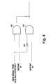
- Fig. 4 provides a more detailed view of one implementation of the selection circuit 8.
- the selection circuit includes two AND gates 54 and 56 and an inverter 60. If the system change- over signal is generated by an external system in response to a switch failure or any other event, the idle cell detector 7 (Fig. 2) swaps the cell switch from which it selects cells by switching the selection switch 8. Those skilled in the art will know of suitable mechanisms for generating such a system change-over signal. During normal operation, a swap signal sent from the idle cell detector 7 to the selection circuit 8 is high. As such, the cells output on line 3a (see Fig.
- the switching is performed only after detector 7 (Fig. 3) confirms that an idle cell is output to the output lines 3a and 4a of both systems.
- the systems are not switched immediately after the system change-over signal is generated but is switched only after an idle is output from both cell switches 11 and 12 to the respective output lines. It is, thus, possible to switch the systems by a very simple circuit structure which neither duplicates nor misses any cells, hence enhancing the throughput of the network.
- cell switches 11 and 12 are shown for illustrative purposes as having four input lines 2a to 2d and four output lines 3a to 3d. It is assumed that each cell has a fixed length, and that cells reach the input lines 2a to 2d at substantially random times, provided that the time interval between cells is equivalent to an integral multiple of the length of a cell. In other words, it is assumed that the input phases of the cells are normalized before they reach input lines 2a to 2d and that the cells are input from all the lines in the same phase.
- Fig. is a timing chart for signals which are input on the input lines 2a to 2d and output to the output lines 3a to 3d.
- the numerals provided at the top of the chart represent time slot numbers. Only one cell is input to one input line for each time slot.
- the numeral at the left portion of each cell represents an output line number
- the numeral at the middle portion of each cell represents an input line number
- the number at the right portion of each cell represents a time slot number.
- the output line numbers 1 to 4 correspond to the output lines 3a to 3d, respectively
- the input line numbers 1 to 4 correspond to the input lines 2a to 2d, respectively.
- the time slot numbers each represents the number of the time slot in which the cell was input.
- the time slots showing no cells are the time slots in which no cell was received or in which an idle cell has been output.
- the cells which are input to the cell switch 11 are distributed to the specified output line numbers and output during the next time slot, as a general rule. If a plurality of cells which are to be delivered to the same output line are input during the same time slot, the cells are output one after another in a predetermined order.
- the order may be determined in various ways. In this illustrative case, a method is employed which outputs the cells according to their input line numbers in a circular order of 1 - 2 - 3 - 4 -. However, this method for ordering the output of the cells is merely illustrative and other approaches may be equally viable.
- both of the cell switches 11 and 12 operate as described above, the order of outputting a plurality of cells which are to be delivered to the same address and which are input during the same time slot is sometimes different, depending upon the internal state of the cell switch. However, there is no time interval between the outputs of the cells. In other words, these plurality of cells are continuously output, and no idle cell is inserted between the cells.
- a plurality of cells when a plurality of cells are to be output to the same output line, they are output in a circular order, as described above.
- the order of outputting the cells is not critical to the present invention. In an extreme case, the cells may be output at random.
- Fig. 6 is a timing chart for signals which are input from the input lines 2a to 2d and output to the output line 3a of cell switch 11 and output line 4a of cell switch 12.
- the input cells are exchanged by the cell switches 11 and 12 so that the cells are output to output lines 3a and 4a.
- the cell received on input line 2a is output to the output line 3a, whereas the cell received on input line 2b is output on the output line 4a during time slot 2.
- the cell switches 11 and 12 exchange cells on the basis of the same control algorithm, but since the internal states of the cell switches 11 and 12 are not always the same, the order of outputting cells in cell switch 11 is sometimes different from the order in the cell switch 12, as shown in Fig. 6 (i.e., note the order in which the cells "111", “121", and “131” " are output on output lines 3a and 4a). In this case, if a changeover to system #2 occurs at time A in Fig. 6, a cell is duplicated or missed, as shown in Fig. 7A.
- the selector 5a (Fig. 3) which is connected to the output lines 3a and 4a receives a system change-over signal
- the selector 5a instructs the selection circuit 8 to switch after the idle cell detector 7 detects an idle cell which is output to the output lines of both systems at time B in Fig. 6. It is, thus, possible to switch systems without duplicating or missing a cell.
- the selectors 5a to 5m (see Fig. 2) switch the systems in this way independently of each other. Therefore, the operation of switching the systems in the entire ATM cell exchanging apparatus as a whole is completed when all the selectors 5a to 5m have finished the switching operation.
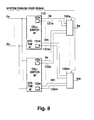
- a cell exchanging apparatus according to a second embodiment of the invention is described in conjunction with Fig. 8.
- Fig. 8 is a block diagram showing the configuration of the cell exchanging apparatus according to the second embodiment of the invention, wherein 2a-2n, 3a-3m, 4a-4m, and 6a-6m are input lines and output lines, as in the first embodiment shown in Fig. 2.
- a cell switch 110 (#1) contains cell monitors 121a-121m;
- a cell switch 120 (#2) contains cell monitors 122a-122m, as a feature of the cell exchanging apparatus according to the second embodiment.
- Each of the cell monitors 121 a-121 m and 122a-122m monitors the output state of a cell to each of switch output lines 3a-3m and 4a-4m, and outputs the monitor result as a cell presence/absence signal to each of cell presence/absence signal lines 131 a-131 m and 132a-132m. If a cell is output, the cell presence/absence signal indicates "cell presence”; if no cell is output, the signal indicates "cell absence".
- selectors 150a-150m used with the second embodiment have a simplified monitor mechanism. Instead, the cell monitors 121 a-121 m and 122a-122m in the cell switches 110 (#1) and 120 (#2) report the monitor results to the selectors 150a-150m. That is, the selectors 150a-150m of the second embodiment do not contain an idle cell detection circuit, and selection circuits are controlled in response to the cell presence/absence signals to the selectors 150a-150m.
- the operation of the cell exchanging apparatus according to the second embodiment is the same as that according to the first embodiment.
- the selectors 150a-150m are responsive to the cell presence/absence signals output by the cell monitors 121 a-121 m and 122a-122m for judging the timing at which an actual change-over can be performed. Entire change-over of the cell switches is completed upon termination of changing over at all the output selectors.
- Idle cells are detected by the output selectors or the cell monitors in the cell switches in the first and second embodiments, but may be detected elsewhere in the cell exchanging apparatus.
- Fig. 9 is a block diagram showing the configuration of the cell exchanging apparatus according to the third embodiment of the invention, wherein the cell exchanging apparatus contains cell switches 110 (#1) and 120 (#2) for exchanging input cells based on their destination information.
- Each of the cells consists of a header section containing an output line number as destination information and a data section containing data to be transmitted.
- each of the cell switches 110 (#1) and 120 (#2) has a buffer memory for each switch output line.
- the buffer memory is an output buffer for once storing cells before they are output to the switch output line corresponding to the buffer memory.
- the cell switch having such output buffers is called an output buffer type switch.
- the cell switch 110 (#1) operates as an active system and the cell switch 120 (#2) operates as a standby system.
- Input lines 2a-2n of the cell exchanging apparatus according to the third embodiment are connected to input selectors 141 a-141 n respectively. Output signals of the input selectors 141a-141n are connected to 151a-151n and 152a-152n, switch input lines of the cell switches 110 (#1) and 120 (#2).
- Switch output lines 3a-3m and 4a-4m, cell exchanging apparatus output lines 6a-6m, and output selectors 150a-150m are the same as those used with the second embodiment.
- cell monitors 121 a-121 m and 122a-122m and cell presence/absence signal lines 131 a-131 m and 132a-132m are the same as those used with the second embodiment.
- the cell exchanging apparatus further includes a controller 160 which grants cell output permission to the cell switch 110 (#1) or 120 (#2) for each switch output line.
- the output permission signals are fed on output permission signal lines 161 and 162 to the cell switches 110 (#1) and 120 (#2).
- the controller 160 grants cell output permission to the cell switch 110 (#1).
- Cells arriving at the cell exchanging apparatus input lines 2a-2n are output through the input selectors 141 a-141n to the switch input lines 151a-151n. Resultantly, the cells are input to the cell switch 110 (#1).
- the cell switch 110 (#1) performs the same operation as the cell switch 110 (#1) in the second embodiment for outputting the cells to the cell output lines 3a-3n.
- the cells output from the cell switch 110 are fed into the output selectors 150a-150m through which the cells are output to the cell exchanging apparatus output lines 6a-6m.
- the cell switch 120 is in the standby mode.
- the input selectors 141 a-141 select the switch input lines 152a-152n. Resultantly, the cells input to the input selectors are all sent to the cell switch 120 (#2) and not sent to the cell switch 110 (#1).
- the cell switch 120 (#2) performs the same processing as the cell switch 110 (#1) for the input cells except that the buffer memories of the cell switch 120 store the cells without outputting them because the cell switch 120 does not yet receive a cell output permission signal from the controller 160.
- Each of the buffer memories is an output buffer provided for each switch output line of the cell switches 110 (#1) and 120 (#2) for storing the cells to be output to the output line corresponding to the buffer.
- the cell switch 110 (#1) still continues to output cells to the switch output lines until the cells stored in the output buffers of the cell switch 110 are out.
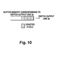
- the cell switch 120 (#2) when the system change-over signal is entered and feeding cells into the cell switch 120 (#2) is started, if four cells are stored in the buffer memory corresponding to the switch output line 3a of the cell switch 110 (#1) as shown in Fig. 10, the cell switch 110 (#1) outputs the cells in sequence.
- the cells which are input to the cell switch 120 (#2) for output to the switch output line 4a are stored in the buffer memory corresponding to the output line 4a.
- the cell presence/absence signal output through the cell presence/absence signal line 131 a is set to a value representing "cell absence" for informing the output selector 150a and the controller 160 that the cells to be output have gone.
- the output selector 150a selects the switch output line 4a instead of the switch output line 3a and the controller 160 sends a cell output permission signal to the cell switch 120 (#2) on the cell output permission signal line 162 for enabling the cells to be output through the switch output line 4a.
- the cell switch 120 (#2) starts to output the cells over the switch output line 4a.
- the third embodiment uses so-called output buffer type ATM switches having a buffer memory for each switch output line as the cell switches 110 (#1 ) and 120 (#2).
- the cell switch contains a buffer memory shared by the switch output lines.
- the cell switch can be operated like the output buffer type ATM switch by managing the addresses of the buffer memory into which cells are written.
- the cell switch having such a shared buffer memory is called a "shared buffer type ATM cell switch.”
- the cell presence/absence monitor function monitors the buffer memory addresses managed for each output line.
- the second embodiment uses so-called output buffer type ATM switches for the cell switches.
Landscapes
- Engineering & Computer Science (AREA)
- Computer Networks & Wireless Communication (AREA)
- Signal Processing (AREA)
- Physics & Mathematics (AREA)
- Mathematical Physics (AREA)
- Data Exchanges In Wide-Area Networks (AREA)
Applications Claiming Priority (3)
| Application Number | Priority Date | Filing Date | Title |
|---|---|---|---|
| JP36189/92 | 1992-02-24 | ||
| JP3618992A JP2671699B2 (ja) | 1991-11-15 | 1992-02-24 | セル交換装置 |
| JP3618992 | 1992-02-24 |
Publications (3)
| Publication Number | Publication Date |
|---|---|
| EP0557910A2 true EP0557910A2 (fr) | 1993-09-01 |
| EP0557910A3 EP0557910A3 (en) | 1995-12-13 |
| EP0557910B1 EP0557910B1 (fr) | 1999-12-29 |
Family
ID=12462783
Family Applications (1)
| Application Number | Title | Priority Date | Filing Date |
|---|---|---|---|
| EP19930102689 Expired - Lifetime EP0557910B1 (fr) | 1992-02-24 | 1993-02-19 | Commutateur de cellules |
Country Status (3)
| Country | Link |
|---|---|
| EP (1) | EP0557910B1 (fr) |
| CA (1) | CA2090101C (fr) |
| DE (1) | DE69327415T2 (fr) |
Cited By (2)
| Publication number | Priority date | Publication date | Assignee | Title |
|---|---|---|---|---|
| GB2383509A (en) * | 2001-12-21 | 2003-06-25 | Agere Systems Inc | Switching between active and standby switch fabrics with no loss of data |
| EP1158733A3 (fr) * | 2000-05-24 | 2004-05-26 | Nec Corporation | Tableau de commutation avec double système de commutation |
Family Cites Families (3)
| Publication number | Priority date | Publication date | Assignee | Title |
|---|---|---|---|---|
| JP2611805B2 (ja) * | 1988-05-13 | 1997-05-21 | 日本電信電話株式会社 | 伝送路切替方式 |
| JP2677418B2 (ja) * | 1989-06-22 | 1997-11-17 | 富士通株式会社 | Atmスイッチの系切換方式 |
| DE69029854T2 (de) * | 1989-11-29 | 1997-06-05 | Fujitsu Ltd | Umschaltverfahren für verdoppeltes atm-vermittlungssystem |
-
1993
- 1993-02-19 EP EP19930102689 patent/EP0557910B1/fr not_active Expired - Lifetime
- 1993-02-19 DE DE1993627415 patent/DE69327415T2/de not_active Expired - Fee Related
- 1993-02-22 CA CA 2090101 patent/CA2090101C/fr not_active Expired - Fee Related
Cited By (4)
| Publication number | Priority date | Publication date | Assignee | Title |
|---|---|---|---|---|
| EP1158733A3 (fr) * | 2000-05-24 | 2004-05-26 | Nec Corporation | Tableau de commutation avec double système de commutation |
| GB2383509A (en) * | 2001-12-21 | 2003-06-25 | Agere Systems Inc | Switching between active and standby switch fabrics with no loss of data |
| GB2383509B (en) * | 2001-12-21 | 2005-03-09 | Agere Systems Inc | Method and apparatus for switching between active and standby switch fabrics with no loss of data |
| US7313089B2 (en) | 2001-12-21 | 2007-12-25 | Agere Systems Inc. | Method and apparatus for switching between active and standby switch fabrics with no loss of data |
Also Published As
| Publication number | Publication date |
|---|---|
| CA2090101C (fr) | 1998-11-24 |
| EP0557910B1 (fr) | 1999-12-29 |
| DE69327415T2 (de) | 2000-05-11 |
| EP0557910A3 (en) | 1995-12-13 |
| CA2090101A1 (fr) | 1993-08-25 |
| DE69327415D1 (de) | 2000-02-03 |
Similar Documents
| Publication | Publication Date | Title |
|---|---|---|
| US5398235A (en) | Cell exchanging apparatus | |
| US5214639A (en) | Communication switching element and method for transmitting variable length cells | |
| US5202885A (en) | Atm exchange with copying capability | |
| AU693084B2 (en) | Controlled access ATM switch | |
| US4761780A (en) | Enhanced efficiency Batcher-Banyan packet switch | |
| US5414696A (en) | Cell exchanging apparatus | |
| EP0858718B1 (fr) | Ameliorations concernant un commutateur mta | |
| US6229789B1 (en) | Congestion avoidance in an ATM switch | |
| US5283782A (en) | System switching method and apparatus without loss of signal in cell switching system of asynchronous transfer mode | |
| EP0828403B1 (fr) | Améliorations dans ou liées à un commutateur ATM | |
| CA2224606C (fr) | Systeme de tampons repartis pour commutateurs mta | |
| EP0415628B1 (fr) | Architecture extensible de commutateur de paquets | |
| IL124011A (en) | Atm switch | |
| US6026098A (en) | Line multiplexing system | |
| JP2629568B2 (ja) | Atmセル交換方式 | |
| US6570845B1 (en) | Switching system including a mask mechanism for altering the internal routing process | |
| US6493315B1 (en) | ATM switch for routing different cell types | |
| US6101184A (en) | Data switching method and data switching apparatus for efficiently handling scan data in information communication network | |
| US5742597A (en) | Method and device for multipoint switching and arbitration in output-request packet switch | |
| US6046982A (en) | Method and apparatus for reducing data loss in data transfer devices | |
| US5402417A (en) | Packet switching system | |
| US6418120B1 (en) | Congestion avoidance mechanism for ATM switches | |
| EP0557910B1 (fr) | Commutateur de cellules | |
| US5724353A (en) | Self-routing switch method and circuit for an ATM switch | |
| JP3197152B2 (ja) | セル交換装置 |
Legal Events
| Date | Code | Title | Description |
|---|---|---|---|
| PUAI | Public reference made under article 153(3) epc to a published international application that has entered the european phase |
Free format text: ORIGINAL CODE: 0009012 |
|
| AK | Designated contracting states |
Kind code of ref document: A2 Designated state(s): DE FR GB SE |
|
| PUAL | Search report despatched |
Free format text: ORIGINAL CODE: 0009013 |
|
| AK | Designated contracting states |
Kind code of ref document: A3 Designated state(s): DE FR GB SE |
|
| 17P | Request for examination filed |
Effective date: 19960118 |
|
| 17Q | First examination report despatched |
Effective date: 19980527 |
|
| GRAG | Despatch of communication of intention to grant |
Free format text: ORIGINAL CODE: EPIDOS AGRA |
|
| GRAG | Despatch of communication of intention to grant |
Free format text: ORIGINAL CODE: EPIDOS AGRA |
|
| GRAH | Despatch of communication of intention to grant a patent |
Free format text: ORIGINAL CODE: EPIDOS IGRA |
|
| GRAH | Despatch of communication of intention to grant a patent |
Free format text: ORIGINAL CODE: EPIDOS IGRA |
|
| GRAA | (expected) grant |
Free format text: ORIGINAL CODE: 0009210 |
|
| AK | Designated contracting states |
Kind code of ref document: B1 Designated state(s): DE FR GB SE |
|
| PG25 | Lapsed in a contracting state [announced via postgrant information from national office to epo] |
Ref country code: SE Free format text: THE PATENT HAS BEEN ANNULLED BY A DECISION OF A NATIONAL AUTHORITY Effective date: 19991229 |
|
| REF | Corresponds to: |
Ref document number: 69327415 Country of ref document: DE Date of ref document: 20000203 |
|
| ET | Fr: translation filed | ||
| PLBE | No opposition filed within time limit |
Free format text: ORIGINAL CODE: 0009261 |
|
| STAA | Information on the status of an ep patent application or granted ep patent |
Free format text: STATUS: NO OPPOSITION FILED WITHIN TIME LIMIT |
|
| 26N | No opposition filed | ||
| REG | Reference to a national code |
Ref country code: GB Ref legal event code: IF02 |
|
| REG | Reference to a national code |
Ref country code: GB Ref legal event code: 746 Effective date: 20020306 |
|
| REG | Reference to a national code |
Ref country code: FR Ref legal event code: D6 |
|
| PGFP | Annual fee paid to national office [announced via postgrant information from national office to epo] |
Ref country code: FR Payment date: 20030210 Year of fee payment: 11 |
|
| PGFP | Annual fee paid to national office [announced via postgrant information from national office to epo] |
Ref country code: GB Payment date: 20030219 Year of fee payment: 11 |
|
| PGFP | Annual fee paid to national office [announced via postgrant information from national office to epo] |
Ref country code: DE Payment date: 20030227 Year of fee payment: 11 |
|
| PG25 | Lapsed in a contracting state [announced via postgrant information from national office to epo] |
Ref country code: GB Free format text: LAPSE BECAUSE OF NON-PAYMENT OF DUE FEES Effective date: 20040219 |
|
| PG25 | Lapsed in a contracting state [announced via postgrant information from national office to epo] |
Ref country code: DE Free format text: LAPSE BECAUSE OF NON-PAYMENT OF DUE FEES Effective date: 20040901 |
|
| GBPC | Gb: european patent ceased through non-payment of renewal fee |
Effective date: 20040219 |
|
| PG25 | Lapsed in a contracting state [announced via postgrant information from national office to epo] |
Ref country code: FR Free format text: LAPSE BECAUSE OF NON-PAYMENT OF DUE FEES Effective date: 20041029 |
|
| REG | Reference to a national code |
Ref country code: FR Ref legal event code: ST |