EP0558243A2 - Convertisseur numérique-analogique produisant une sortie linéaire précise aussi bien pour des entrées de signal numérique positives que négatives - Google Patents
Convertisseur numérique-analogique produisant une sortie linéaire précise aussi bien pour des entrées de signal numérique positives que négatives Download PDFInfo
- Publication number
- EP0558243A2 EP0558243A2 EP93301262A EP93301262A EP0558243A2 EP 0558243 A2 EP0558243 A2 EP 0558243A2 EP 93301262 A EP93301262 A EP 93301262A EP 93301262 A EP93301262 A EP 93301262A EP 0558243 A2 EP0558243 A2 EP 0558243A2
- Authority
- EP
- European Patent Office
- Prior art keywords
- circuit
- operational amplifier
- currents
- output
- providing
- Prior art date
- Legal status (The legal status is an assumption and is not a legal conclusion. Google has not performed a legal analysis and makes no representation as to the accuracy of the status listed.)
- Ceased
Links
- 238000000034 method Methods 0.000 claims abstract description 35
- 238000006243 chemical reaction Methods 0.000 claims abstract description 19
- 230000008878 coupling Effects 0.000 claims 2
- 238000010168 coupling process Methods 0.000 claims 2
- 238000005859 coupling reaction Methods 0.000 claims 2
- 238000010586 diagram Methods 0.000 description 4
- 230000003321 amplification Effects 0.000 description 3
- 238000003199 nucleic acid amplification method Methods 0.000 description 3
- 238000009966 trimming Methods 0.000 description 2
- 238000004883 computer application Methods 0.000 description 1
- 230000010354 integration Effects 0.000 description 1
- 239000004065 semiconductor Substances 0.000 description 1
Images

Classifications
-
- H—ELECTRICITY
- H03—ELECTRONIC CIRCUITRY
- H03M—CODING; DECODING; CODE CONVERSION IN GENERAL
- H03M1/00—Analogue/digital conversion; Digital/analogue conversion
- H03M1/66—Digital/analogue converters
- H03M1/74—Simultaneous conversion
- H03M1/742—Simultaneous conversion using current sources as quantisation value generators
- H03M1/745—Simultaneous conversion using current sources as quantisation value generators with weighted currents
Definitions
- This invention relates to improvements in methods and circuitry for converting digital numbers to analog output signals, and more particularly to improvements in methods and circuitry for converting a signed digital number to an analog output signal while maintaining an output offset voltage typically equal to the input offset voltage of only one operational amplifier to produce a precise linear output for both positive and negative digital input values.
- This invention pertains to digital to analog (D/A) conversion in which an input number is a binary-coded or two's-complement digital number which is considered to be "bipolar", representing either a positive or negative number with the most significant bit (MSB) of the digital word being the "sign" bit.
- An analog ground, or zero voltage reference signal is usually provided by the user external to the digital to analog converter, and the internal conversion in the D/A device may be generated based on a different reference voltage level. Therefore, it is often necessary to convert the output of the D/A converter to the reference provided by the user. This unfortunately entails the generation of offset voltages created by level-shifting and amplification which are difficult to minimize, and therefore creates an undesirable error in the output voltage for a given input number. This is unsatisfactory because precision is usually important in D/A conversion.
- the invention presents a circuit for converting a digital number having a positive or negative sign to an analog output signal.
- the circuit includes switching circuitry for producing weighted currents representing bits that have a predetermined state for combination into a sum current, conversion circuitry for converting said sum current into a voltage with a polarity with respect to a reference voltage corresponding to the sign of said digital number, and switching circuitry for selectively delivering the sum current to a selected input of said conversion circuitry depending on the sign of the digital number for the purpose of determining the polarity with respect to said reference voltage of the analog output signal.
- a method for converting a signed digital number to an analog output signal is presented.
- weighted bit currents are produced representing the bits of the digital number for combination into a sum current
- a circuit is provided for converting the sum current to an output voltage that has a polarity with respect to a reference voltage determined by the sign of the digital number.
- the sum current is selectively delivered to a selected input of the circuitry for converting the sum current into a voltage depending on the sign of the digital number for the purpose of determining the polarity with respect to said reference voltage of the analog output signal.
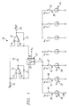
- Figure 1 is an electrical schematic diagram of a digital to analog conversion system incorporating apparatus in accordance with one embodiment of the invention, utilizing amplitude plus sign coding.
- Figure 2 is an electrical schematic diagram of a digital to analog conversion system for a two's-complement configuration incorporating apparatus in accordance with another embodiment of the invention.
- FIG. 1 An electrical schematic diagram of a digital to analog converter 10 in which the apparatus and method in accordance with a preferred embodiment of the invention is incorporated is shown in Figure 1.
- This digital to analog converter 10 has input lines b0 ... b7 to receive a standard binary input number.
- the digital to analog converter 10 can be constructed of discrete components, preferably, it is integrated onto a single integrated circuit.
- the binary input number received on the parallel input lines b0 ... b7 may represent either a positive or negative digital number.
- the sign of the number is indicated by the "sign bit", which typically is the most significant bit (MSB), and which appears on the input line b7.
- the data lines 30, 31, 32, ... 35 carry "binary-weighted” currents, or weighted bit currents, the magnitude of the current on each line of which corresponding to the value, or power, of the binary bit applied to the respective input lines b0 ... b6.
- current sources 36, 37, 38, ... 41 generate particular values of current on the respective input lines representing the least significant bit (LSB) (20), twice that value on the next most significant bit (21), four times that value on the next (22), and so on.
- the currents provided by the current sources 36 - 41 are controlled by switches 45, 46, 47, ... 50, which are typically transistor switches, but which may be realized by any appropriate type of switch.
- switches 45, 46, 47, ... 50 which are typically transistor switches, but which may be realized by any appropriate type of switch.
- a logical "1" on one of the input lines causes its respective one of switches 45, 46, 47, ... 50 to close;
- a logical "0" on one of the input lines causes its respective one of switches 45, 46, 47, ... 50 to open.
- the current appearing at the node 51 will be the sum of the currents selectively connected thereto by the operation of the selected ones of the switches 45 - 50.
- switches 45, 46, 47, ... 50 and current generators 36, 37, 38, ... 41 are shown, both the switch and current generator in each path may be realized by one set of appropriately sized transistors or equivalent devices.
- the sign bit i.e., the most significant bit on the line b6, activates a switch 27 that selectively directs the currents summed at the node 51 to the inverting input 16 of a first operational amplifiers 15 when the sign bit is negative, or to the inverting input of the operational amplifier 21 when the sign bit is positive.
- the operational amplifiers 15 and 21 are connected in a transresistance configuration as current to voltage converters, where the second operational amplifier 21 is also acting as a buffer, providing a low-impedance output.
- a reference voltage 12 is impressed on the noninverting inputs 13 and 14 of the operational amplifiers 15 and 21; as noted previously, since this voltage may be different from the user-supplied analog ground (zero reference signal), level-shifting may be necessary.
- the two operational amplifiers 15 and 21 are configured with feedback resistors 17 and 23 to minimize the output error voltage.
- the circuit can be realized with resistors 17 and 23 being of substantially equal value, the closer to equal they can be made the better the precision that can be realized in the operation of the circuit.
- the signal from the first operational amplifier 15 is coupled by a resistor 19 to the noninverting input 18 of the second operational amplifier 21.
- the configuration is such that for a no-input condition the output offset voltage is typically no more than the equivalent input offset voltage of a unity-gain configuration of only one of the two operational amplifiers. In fact, if the two operational amplifiers are identical and have the same input offset voltage the output offset is exactly equal to the input offset voltage, regardless of the gain (output range of the digital to analog converter).
- the accurate matching of positive and negative output voltages corresponding to positive and negative digital numbers is only limited by the precision of the operational amplifier feedback resistors 17 and 23, provided the open loop gain of the operational amplifiers 15 and 21 is sufficiently high.
- FIG. 2 An electrical schematic diagram of a digital to analog converter 60 in which the apparatus and method in accordance with another preferred embodiment of the invention is incorporated is shown in Figure 2.
- the digital to analog converter 60 can be constructed of discrete components; however, preferably it is integrated onto a single integrated circuit device adapted for connection within a larger system.
- the input to the circuit 60 is a binary number presented on the parallel data lines d0 - d7.
- the currents are weighted according to their respective binary values, with the state of the most significant bit d7 controlling a switch 62 that routes or "steers" the summed current either to the inverting input 63 or 64 of respective operational amplifier 65 or 66 for conversion to an output voltage 67.
- the amplifiers 65 and 66 are serially connected in a chain configuration, with a reference voltage 71 applied to the noninverting inputs 72 and 73 of the respective operational amplifiers 65 and 66.
- Feedback resistors 74 and 75 are connected between the outputs and inverting inputs of each of the amplifiers 65 and 66.
- resistors 74 and 75 are of substantially equal value, the closer to equal they can be made the better the precision that can be realized in the operation of the circuit.
- Another resistor 76 couples the output of the first operation amplifier 65 to the second operational amplifier 66.
- this D/A converter circuit 60 differs from the embodiment described above with reference to Figure 1 in that the analog voltage output will be an analog signal corresponding to the two's-complement representation of the input binary number.
- This particular embodiment is particularly useful in modern electronics and computer applications, since most computers currently use the two's-complement system for computations.
- a decoding circuit 80 is provided to perform this conversion and a current weighting function for negative binary input numbers, as well as to perform a current weighting function for positive binary input numbers.
- the decoding circuitry 80 includes switches 81 - 87, which may be realized using transistors or other switching devices, that are operated to switch to the left poles 90 - 96 if the state of the respective binary bit on inputs d0 - d6 is a logic "0", and to switch to the right poles 100 - 106 if the state of the respective binary bit on inputs d0 - d6 is a logic "1".
- Each of the switches has a current source connected in series with it, having a current weighted according to the bit position to which the switch 81 - 87 corresponds.
- current sources 120 - 126 generate particular values of current on the respective input lines representing the least significant bit (LSB), twice that value on the next most significant bit, four times that value on the next, and so on.
- the switch 62 operates to route the bit currents summed on the nodes 110 and 111 as controlled by the most significant bit (sign bit) on the input terminal d7.
- the switch 62 connects the node 111 to the inverting input 63 of the operational amplifier 65 (and the node 110 to V cc ).
- the switch 62 connects the node 110 to the inverting input 64 of the operational amplifier 66, and connects the node 111 to V cc .
- the weighted currents representing bits having a value of logical "0" are routed through the left-hand poles 90 - 96 through the negative sum line 130 to be summed on node 111 and directed to the V cc termination 55.
- the weighted currents representing bits having a value of logical "1" are connected by the right-hand poles 100 - 106 to the positive sum line 131 to be summed on the node 110 and directed via the switch 62 to the inverting input 64 of the right-band operational amplifier 66 for conversion into an analog output voltage 67 corresponding to the positive binary number on the input lines d0 - d7.
Landscapes
- Engineering & Computer Science (AREA)
- Theoretical Computer Science (AREA)
- Analogue/Digital Conversion (AREA)
Applications Claiming Priority (2)
| Application Number | Priority Date | Filing Date | Title |
|---|---|---|---|
| US07/843,578 US5296857A (en) | 1992-02-28 | 1992-02-28 | Digital to analog converter with precise linear output for both positive and negative digital input values |
| US843578 | 1992-02-28 |
Publications (2)
| Publication Number | Publication Date |
|---|---|
| EP0558243A2 true EP0558243A2 (fr) | 1993-09-01 |
| EP0558243A3 EP0558243A3 (en) | 1994-09-28 |
Family
ID=25290430
Family Applications (1)
| Application Number | Title | Priority Date | Filing Date |
|---|---|---|---|
| EP9393301262A Ceased EP0558243A3 (en) | 1992-02-28 | 1993-02-22 | Digital to analog converter with precise linear output for both positive and negative digital input values |
Country Status (3)
| Country | Link |
|---|---|
| US (1) | US5296857A (fr) |
| EP (1) | EP0558243A3 (fr) |
| JP (1) | JPH0621814A (fr) |
Cited By (1)
| Publication number | Priority date | Publication date | Assignee | Title |
|---|---|---|---|---|
| GB2344479A (en) * | 1998-12-04 | 2000-06-07 | Asahi Chemical Ind | Resistor-type D/A convertor having a highly linear transconductor |
Families Citing this family (8)
| Publication number | Priority date | Publication date | Assignee | Title |
|---|---|---|---|---|
| US5543697A (en) * | 1994-10-27 | 1996-08-06 | Sgs-Thomson Microelectronics, Inc. | Circuit and method for controlling the speed of a motor |
| US5617473A (en) * | 1995-06-23 | 1997-04-01 | Harris Corporation | Sign bit integrator and method |
| US5805095A (en) * | 1997-01-10 | 1998-09-08 | Motorola, Inc. | Two's complement digital to analog converter |
| JP4113758B2 (ja) | 2002-10-29 | 2008-07-09 | 株式会社イシダ | 重量測定装置、ノイズ除去方法およびディジタルフィルタの設計方法 |
| US6879276B2 (en) * | 2003-08-14 | 2005-04-12 | Telasic Communications, Inc. | Split cell bowtie digital to analog converter and method |
| WO2006039510A2 (fr) * | 2004-09-30 | 2006-04-13 | The Trustees Of Columbia University In The City Ofnew York | Amplificateur numerique a temps continu |
| JP5440143B2 (ja) * | 2009-12-16 | 2014-03-12 | ヤマハ株式会社 | 電圧加算回路およびd/a変換回路 |
| US10073167B2 (en) * | 2015-05-22 | 2018-09-11 | Texas Instruments Incorporated | High speed illumination driver for TOF applications |
Family Cites Families (4)
| Publication number | Priority date | Publication date | Assignee | Title |
|---|---|---|---|---|
| US3924229A (en) * | 1969-01-10 | 1975-12-02 | Ibm | Bipolar digital to analog converter utilizing two reference voltages of the same polarity |
| US3685045A (en) * | 1969-03-24 | 1972-08-15 | Analog Devices Inc | Digital-to-analog converters |
| DE2011056B2 (de) * | 1970-03-09 | 1971-12-16 | Krone Gmbh, 1000 Berlin | Pulscodedemodulator mit dehnercharakteristik aufweisender knickkennlinie |
| US4410880A (en) * | 1981-03-25 | 1983-10-18 | Sperry Corporation | Digital-to-analog converter and analog-to-digital converter with controllable bi-polar and uni-polar capability |
-
1992
- 1992-02-28 US US07/843,578 patent/US5296857A/en not_active Expired - Lifetime
-
1993
- 1993-02-22 EP EP9393301262A patent/EP0558243A3/en not_active Ceased
- 1993-02-26 JP JP5038962A patent/JPH0621814A/ja active Pending
Cited By (2)
| Publication number | Priority date | Publication date | Assignee | Title |
|---|---|---|---|---|
| GB2344479A (en) * | 1998-12-04 | 2000-06-07 | Asahi Chemical Ind | Resistor-type D/A convertor having a highly linear transconductor |
| US6346899B1 (en) | 1998-12-04 | 2002-02-12 | Asahi Kasei Kabushiki Kaisha | Analog current mode D/A converter using transconductors |
Also Published As
| Publication number | Publication date |
|---|---|
| US5296857A (en) | 1994-03-22 |
| EP0558243A3 (en) | 1994-09-28 |
| JPH0621814A (ja) | 1994-01-28 |
Similar Documents
| Publication | Publication Date | Title |
|---|---|---|
| JP2819006B2 (ja) | サーモメータ・バイナリ・エンコード方法 | |
| US5585795A (en) | D/A converter including output buffer having a controllable offset voltage | |
| EP0493443B1 (fr) | CONVERTISSEUR ANALOGIQUE-NUMERIQUE PARALLELE UTILISANT 2?n-1 COMPARATEURS | |
| KR101476119B1 (ko) | 다입력 연산 증폭회로, 그것을 사용한 디지털/아날로그변환기 및 그것을 사용한 표시장치의 구동회로 | |
| EP0708530A1 (fr) | Convertisseur numérique-analogique alimenté par source de courant et convertisseur analogique-numérique utilisant un tel convertisseur numérique-analogique | |
| US6392574B1 (en) | System and method for exponential digital to analog conversion | |
| US5459466A (en) | Method and apparatus for converting a thermometer code to a gray code | |
| US5296857A (en) | Digital to analog converter with precise linear output for both positive and negative digital input values | |
| EP0378840A2 (fr) | Convertisseur numérique-analogique à chaîne résistive unique à tension réglable à travers ladite chaîne | |
| JPS5972226A (ja) | 符号化回路 | |
| USRE38083E1 (en) | Rail-to-rail DAC drive circuit | |
| JP3059859B2 (ja) | 符号−絶対値形d/aコンバータ及びその動作方法 | |
| EP0743758B1 (fr) | Convertisseur numérique-analogique quadratique | |
| US3832707A (en) | Low cost digital to synchro converter | |
| KR960016011B1 (ko) | A/d 변환기 | |
| JPH10501115A (ja) | 信号に依存するオフセットを有する作動増幅器及びこのような作動増幅器を含むマルチステップ2重残差アナログ−デジタルコンバータ | |
| US6208278B1 (en) | System and method for logarithmic digital to analog conversion | |
| EP0952672A2 (fr) | Circuit de conversion analogique-numérique et dispositif de conversion analogique-numérique utilisant ce circuit | |
| KR20020064321A (ko) | 디지털/아날로그 변환기 | |
| EP0135274A2 (fr) | Convertisseur numérique-analogique | |
| JPH06132828A (ja) | D/a変換装置 | |
| JPH06268523A (ja) | D/a変換器 | |
| CN110022110B (zh) | 音圈马达阻尼控制电路 | |
| JPH08307273A (ja) | D/aコンバータ回路 | |
| US4529966A (en) | High-speed bipolar logarithmic analog-to-digital converter |
Legal Events
| Date | Code | Title | Description |
|---|---|---|---|
| PUAI | Public reference made under article 153(3) epc to a published international application that has entered the european phase |
Free format text: ORIGINAL CODE: 0009012 |
|
| AK | Designated contracting states |
Kind code of ref document: A2 Designated state(s): DE FR GB IT |
|
| PUAL | Search report despatched |
Free format text: ORIGINAL CODE: 0009013 |
|
| AK | Designated contracting states |
Kind code of ref document: A3 Designated state(s): DE FR GB IT |
|
| 17P | Request for examination filed |
Effective date: 19950321 |
|
| 17Q | First examination report despatched |
Effective date: 19970407 |
|
| GRAG | Despatch of communication of intention to grant |
Free format text: ORIGINAL CODE: EPIDOS AGRA |
|
| RAP3 | Party data changed (applicant data changed or rights of an application transferred) |
Owner name: STMICROELECTRONICS, INC. |
|
| STAA | Information on the status of an ep patent application or granted ep patent |
Free format text: STATUS: THE APPLICATION HAS BEEN REFUSED |
|
| 18R | Application refused |
Effective date: 19990308 |