EP0558801B1 - Wellelängenwandlervorrichtung - Google Patents
Wellelängenwandlervorrichtung Download PDFInfo
- Publication number
- EP0558801B1 EP0558801B1 EP92117915A EP92117915A EP0558801B1 EP 0558801 B1 EP0558801 B1 EP 0558801B1 EP 92117915 A EP92117915 A EP 92117915A EP 92117915 A EP92117915 A EP 92117915A EP 0558801 B1 EP0558801 B1 EP 0558801B1
- Authority
- EP
- European Patent Office
- Prior art keywords
- optical waveguide
- waveguide
- wavelength
- harmonic
- voltage
- Prior art date
- Legal status (The legal status is an assumption and is not a legal conclusion. Google has not performed a legal analysis and makes no representation as to the accuracy of the status listed.)
- Expired - Lifetime
Links
- 230000003287 optical effect Effects 0.000 claims description 41
- 230000010287 polarization Effects 0.000 claims description 16
- 239000000758 substrate Substances 0.000 claims description 9
- 230000000737 periodic effect Effects 0.000 claims description 6
- 239000013078 crystal Substances 0.000 claims description 5
- 230000005684 electric field Effects 0.000 description 7
- 230000005693 optoelectronics Effects 0.000 description 6
- 229910003327 LiNbO3 Inorganic materials 0.000 description 2
- WSMQKESQZFQMFW-UHFFFAOYSA-N 5-methyl-pyrazole-3-carboxylic acid Chemical compound CC1=CC(C(O)=O)=NN1 WSMQKESQZFQMFW-UHFFFAOYSA-N 0.000 description 1
- 229910012463 LiTaO3 Inorganic materials 0.000 description 1
- XAGFODPZIPBFFR-UHFFFAOYSA-N aluminium Chemical compound [Al] XAGFODPZIPBFFR-UHFFFAOYSA-N 0.000 description 1
- 229910052782 aluminium Inorganic materials 0.000 description 1
- 238000006243 chemical reaction Methods 0.000 description 1
- 230000003247 decreasing effect Effects 0.000 description 1
- GQYHUHYESMUTHG-UHFFFAOYSA-N lithium niobate Chemical compound [Li+].[O-][Nb](=O)=O GQYHUHYESMUTHG-UHFFFAOYSA-N 0.000 description 1
- 238000000034 method Methods 0.000 description 1
- 239000004065 semiconductor Substances 0.000 description 1
Images

Classifications
-
- G—PHYSICS
- G02—OPTICS
- G02F—OPTICAL DEVICES OR ARRANGEMENTS FOR THE CONTROL OF LIGHT BY MODIFICATION OF THE OPTICAL PROPERTIES OF THE MEDIA OF THE ELEMENTS INVOLVED THEREIN; NON-LINEAR OPTICS; FREQUENCY-CHANGING OF LIGHT; OPTICAL LOGIC ELEMENTS; OPTICAL ANALOGUE/DIGITAL CONVERTERS
- G02F1/00—Devices or arrangements for the control of the intensity, colour, phase, polarisation or direction of light arriving from an independent light source, e.g. switching, gating or modulating; Non-linear optics
- G02F1/35—Non-linear optics
- G02F1/37—Non-linear optics for second-harmonic generation
- G02F1/377—Non-linear optics for second-harmonic generation in an optical waveguide structure
- G02F1/3775—Non-linear optics for second-harmonic generation in an optical waveguide structure with a periodic structure, e.g. domain inversion, for quasi-phase-matching [QPM]
-
- G—PHYSICS
- G02—OPTICS
- G02F—OPTICAL DEVICES OR ARRANGEMENTS FOR THE CONTROL OF LIGHT BY MODIFICATION OF THE OPTICAL PROPERTIES OF THE MEDIA OF THE ELEMENTS INVOLVED THEREIN; NON-LINEAR OPTICS; FREQUENCY-CHANGING OF LIGHT; OPTICAL LOGIC ELEMENTS; OPTICAL ANALOGUE/DIGITAL CONVERTERS
- G02F1/00—Devices or arrangements for the control of the intensity, colour, phase, polarisation or direction of light arriving from an independent light source, e.g. switching, gating or modulating; Non-linear optics
- G02F1/35—Non-linear optics
- G02F1/353—Frequency conversion, i.e. wherein a light beam is generated with frequency components different from those of the incident light beams
- G02F1/3544—Particular phase matching techniques
- G02F1/3546—Active phase matching, e.g. by electro- or thermo-optic tuning
-
- G—PHYSICS
- G02—OPTICS
- G02F—OPTICAL DEVICES OR ARRANGEMENTS FOR THE CONTROL OF LIGHT BY MODIFICATION OF THE OPTICAL PROPERTIES OF THE MEDIA OF THE ELEMENTS INVOLVED THEREIN; NON-LINEAR OPTICS; FREQUENCY-CHANGING OF LIGHT; OPTICAL LOGIC ELEMENTS; OPTICAL ANALOGUE/DIGITAL CONVERTERS
- G02F2201/00—Constructional arrangements not provided for in groups G02F1/00 - G02F7/00
- G02F2201/06—Constructional arrangements not provided for in groups G02F1/00 - G02F7/00 integrated waveguide
-
- G—PHYSICS
- G02—OPTICS
- G02F—OPTICAL DEVICES OR ARRANGEMENTS FOR THE CONTROL OF LIGHT BY MODIFICATION OF THE OPTICAL PROPERTIES OF THE MEDIA OF THE ELEMENTS INVOLVED THEREIN; NON-LINEAR OPTICS; FREQUENCY-CHANGING OF LIGHT; OPTICAL LOGIC ELEMENTS; OPTICAL ANALOGUE/DIGITAL CONVERTERS
- G02F2202/00—Materials and properties
- G02F2202/20—LiNbO3, LiTaO3
Definitions
- the present invention relates to wavelength converting elements wherein the second harmonic of the fundamental wave is generated by a laser beam.
- QPM quasi phase matching
- the wavelength converting element comprises an optical waveguide in the substrate made of a non-linear optical crystal.
- the optical waveguide has a periodic polarization inversion structure wherein the polarization inverts periodically.
- Such an element utilizing QPM has a considerably small degree of allowability for fundamental wavelength.
- the phase matching conditions may not therefore be satisfied in some cases.
- the degree of allowability of wavelength to the fundamental wave is as narrow as about 0.2 nm, the fundamental wavelength control becomes strict, and demanding high precision in the dimension of the period polarization inversion layer.
- wavelength converting elements as designed to have waveguide parameters such as the dimensions of an optical waveguide and the polarization inversion period gradually varying along the optical waveguide, as disclosed in, for example, Japanese Patent Laid-open No. 2-282232 and 3-31828.
- wavelength converting elements Although the structures of wavelength converting elements disclosed in those Japanese patent Laid-opens relax the phase matching conditions, they may reduce the efficiency of converting the fundamental wave to a second harmonic. If the degree of a change in the waveguide parameter in the optical waveguide is increased to expand the degree of allowability of wavelength, the conversion efficiency is considerably decreased so that the elements may not be put into practical use.
- the wavelength converting element comprises an optical waveguide formed in a substrate made of a non-linear optical crystal with at least one of waveguide parameters varying with small degree along the waveguiding direction, said optical waveguide having a periodic polarization inversion region along the waveguiding direction, and further comprises voltage applying means for applying a voltage to at least the optical waveguide to thereby control at least one of the waveguide parameters.
- At least one of multiple waveguide parameters varies with small degree along the optical waveguide formed in the substrate. Further, a voltage is applied to at least the optical waveguide so that the optical waveguide is set in an electric field.
- the waveguide parameter of each of the fundamental wave and second harmonic in the optical waveguide such as refractive index, is controlled by an electrooptical effect induced from that electric field, so that the phase matching conditions in relaxed. Furthermore, the efficiency of converting the fundamental wave to the second harmonic is improved by making the change in the waveguide parameter smaller.
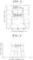
- reference numeral "1" denotes a substrate made of lithium niobate (LiNbO3) as a non-linear optical crystal, the thickness direction of the substrate 1 matching with the direction of the c axis.
- An optical waveguide 2 which extends in the waveguiding direction of light is formed on a c surface, which is one major surface 1a of the substrate 1.
- the waveguide 2 is made by a proton exchange method, for example.
- the optical waveguide 2 has a periodic polarization inversion region 3 where each polarization of small volume is periodically inverted along the optical waveguide 2.
- the period ⁇ of polarization inversion as one waveguide parameter gradually becomes shorter toward a light-emitting end 2b of the optical waveguide 2 from a light-incident end 2a thereof, as shown in Fig. 2.
- a buffer layer 4 made of a dielectric is formed on one major surface 1a, and an electrode 5 made of, for example, aluminum (Al) is deposited on the buffer layer 4. Further, an electrode 6 is formed on the other major surface 1b of the substrate 1, faced the electrode 5, in a similar manner.
- the electrodes 5 and 6 facing each other via the optical waveguide 2 are connected to a power supply 7 to thereby constitute voltage applying means for applying a voltage to the optical waveguide 2 along the c axis, which is perpendicular to the waveguiding direction of the optical waveguide 2.
- a laser beam emitted from, for example, a semiconductor laser enters, as the fundamental wave, the light-incident end 2a of the optical waveguide 2. As the laser beam travels through the optical waveguide 2, it generates a second harmonic which is in turn output from the light-emitting end 2b.
- the degree of allowability of wavelength with respect to a change in the fundamental wavelength becomes larger as compared with that of an element whose polarization is inverted at a constant period.
- the allowable wavelength band ⁇ w which satisfies the phase matching conditions becomes wider as shown in Fig. 3. In other words, the phase matching conditions are relaxed.
- the optical waveguide 2 since a voltage is applied to the optical waveguide 2 perpendicular to the waveguiding direction, the optical waveguide 2 is in an electric field. An electrooptical effect is induced from that electric field so that the refractive indices of the fundamental wave and second harmonic in the optical waveguide, n F and n SH , relating to the c axis are varied. If the fundamental wave falls out of the allowable wavelength band ⁇ w when no voltage applied, changing the individual refractive indices n F and n SH by the applied-voltage induced electrooptical effect shifts this allowable fundamental wavelength band ⁇ w toward the short wavelength side or long wavelength side in accordance with the applied voltage. As the fundamental wavelength of the allowable wavelength band ⁇ w is included in the allowable wavelength band shifted by the electrooptical effect, the phase matching conditions are satisfied so that the second harmonic can be increased. Further, the efficiency of converting the fundamental wave to the second harmonic can be improved.
- a non-linear optical crystal such as lithium tantalate (LiTaO3) may be used instead of LiNbO3.
- the waveguide parameter that varies along the waveguiding direction may be the width of the optical waveguide 2, or the thickness of the optical waveguide 2, or a combination of at least two of the three parameters: the width and thickness of the optical waveguide 2 and the pitch ⁇ of the inversion period.
- the voltage applying means is not limited to have the above-described structure, but other proper voltage applying means may be used as long as the electric field is parallel to the polarization in the optical waveguide 2.
- the application of a voltage by the voltage applying means forces the optical waveguide to be in an electric field
- the waveguide parameters of the fundamental wave and second harmonic in the optical waveguide such as refractive indices
- the waveguide parameters of the fundamental wave and second harmonic in the optical waveguide can be controlled by an electrooptical effect induced from that electric field. It is therefore possible to expand the allowable fundamental wavelength band which satisfies the phase matching conditions. Further, this allowable fundamental wavelength band can be shifted toward the short wavelength side or long wavelength side in accordance with the level of the applied voltage. Even with the fundamental wave whose wavelength is off the allowable wavelength band, therefore, the application of a voltage can set the fundamental wavelength within the allowable wavelength band to thereby meet the phase matching conditions. The efficiency of converting the fundamental wave to the second harmonic can thus be improved.
Landscapes
- Physics & Mathematics (AREA)
- Nonlinear Science (AREA)
- General Physics & Mathematics (AREA)
- Optics & Photonics (AREA)
- Optical Integrated Circuits (AREA)
Claims (1)
- Wellenlängenwandlerelement umfassend:einen optischen Wellenleiter (2), der in einem Substrat (1) gebildet ist, das aus einem nichtlinearen optischen Kristall besteht, wobei sich zumindest einer der Wellenleiterparameter entlang einer Wellenleitungsrichtung ändert, wobei der optische Wellenleiter (2) einen periodischen Wellenleiterumkehrungsbereich (3) entlang der Wellenleitungsrichtung aufweist, gekennzeichnet durcheine Spannungsanlegungseinrichtung (5, 6) zum Anlegen einer Spannung an zumindest den optischen Wellenleiter (2), um dadurch zumindest einen der Wellenleiterparameter zu steuern.
Applications Claiming Priority (2)
| Application Number | Priority Date | Filing Date | Title |
|---|---|---|---|
| JP48765/92 | 1992-03-05 | ||
| JP4048765A JPH05249518A (ja) | 1992-03-05 | 1992-03-05 | 波長変換素子 |
Publications (2)
| Publication Number | Publication Date |
|---|---|
| EP0558801A1 EP0558801A1 (de) | 1993-09-08 |
| EP0558801B1 true EP0558801B1 (de) | 1996-05-15 |
Family
ID=12812376
Family Applications (1)
| Application Number | Title | Priority Date | Filing Date |
|---|---|---|---|
| EP92117915A Expired - Lifetime EP0558801B1 (de) | 1992-03-05 | 1992-10-20 | Wellelängenwandlervorrichtung |
Country Status (3)
| Country | Link |
|---|---|
| EP (1) | EP0558801B1 (de) |
| JP (1) | JPH05249518A (de) |
| DE (1) | DE69210799T2 (de) |
Families Citing this family (7)
| Publication number | Priority date | Publication date | Assignee | Title |
|---|---|---|---|---|
| GB2287327A (en) * | 1994-03-02 | 1995-09-13 | Sharp Kk | Electro-optic apparatus |
| DE19514823C1 (de) * | 1995-04-21 | 1996-11-14 | Fraunhofer Ges Forschung | Vorrichtung zum Vervielfachen von Lichtfrequenzen |
| JP4806114B2 (ja) * | 1999-05-14 | 2011-11-02 | パナソニック株式会社 | 光波長変換素子並びにそれを使用したレーザ光発生装置及び光情報処理装置 |
| US7999998B2 (en) | 2006-10-27 | 2011-08-16 | Panasonic Corporation | Short wavelength light source and laser image forming apparatus |
| CN101646976B (zh) | 2007-03-22 | 2012-09-26 | 松下电器产业株式会社 | 激光波长转换装置以及具备该激光波长转换装置的图像显示装置 |
| US7781779B2 (en) * | 2007-05-08 | 2010-08-24 | Luminus Devices, Inc. | Light emitting devices including wavelength converting material |
| EP2192443B1 (de) | 2007-09-12 | 2012-07-18 | Mitsubishi Electric Corporation | Wellenlängenumsetzungselement und wellenlängenumsetzungs-laseranordnung |
Family Cites Families (1)
| Publication number | Priority date | Publication date | Assignee | Title |
|---|---|---|---|---|
| FR2385114A1 (fr) * | 1977-03-23 | 1978-10-20 | Thomson Csf | Dispositif optique non lineaire en couche mince et son procede de fabrication |
-
1992
- 1992-03-05 JP JP4048765A patent/JPH05249518A/ja active Pending
- 1992-10-20 DE DE69210799T patent/DE69210799T2/de not_active Expired - Fee Related
- 1992-10-20 EP EP92117915A patent/EP0558801B1/de not_active Expired - Lifetime
Also Published As
| Publication number | Publication date |
|---|---|
| DE69210799D1 (de) | 1996-06-20 |
| EP0558801A1 (de) | 1993-09-08 |
| JPH05249518A (ja) | 1993-09-28 |
| DE69210799T2 (de) | 1996-09-26 |
Similar Documents
| Publication | Publication Date | Title |
|---|---|---|
| EP0664474B1 (de) | Elektrisch abstimmbares Gitter und optische Elemente mit einem solchen Gitter | |
| US6914999B2 (en) | Electro-optic modulators | |
| US6353690B1 (en) | Electrically adjustable diffraction grating | |
| EP0683535A1 (de) | Generator nicht linear optischer Strahlung und Verfahren zur Steuerung Gegenden in von ferroelektrischen Polarisationsgebieten in Festkörpern | |
| EP0485159B1 (de) | Verfahren zur Herstellung einer Wellenleitervorrichtung zur Erzeugung der zweiten Harmonischen | |
| JP3036255B2 (ja) | 光波長変換素子およびそれを用いた短波長レーザ光源および短波長レーザ光源を用いた光情報処理装置および光波長変換素子の製造方法 | |
| EP0558801B1 (de) | Wellelängenwandlervorrichtung | |
| EP0962809B1 (de) | Vorrichtung zur Erzeugung der zweiten harmonischen Welle | |
| JPH0419719A (ja) | 非線形強誘電体光学材料に対するドメイン制御方法 | |
| JPS6149649B2 (de) | ||
| US5103491A (en) | Waveguide type optical circuit element | |
| EP0433487A1 (de) | Vorrichtung zur Erzeugung der zweiten Harmonischen | |
| JPS57158616A (en) | Optical coupler | |
| JPH05341344A (ja) | 波長変換素子 | |
| JP2643735B2 (ja) | 波長変換素子 | |
| JPH0651359A (ja) | 波長変換素子、短波長レーザ装置および波長可変レーザ装置 | |
| JPH06110024A (ja) | 光反射器 | |
| JPH0566440A (ja) | レーザ光源 | |
| Petrov | Acoustooptic and electrooptic guided wave conversion to leaky waves in an anisotropic optical waveguide | |
| JP2658381B2 (ja) | 導波路型波長変換素子 | |
| JPH05333391A (ja) | 波長変換素子 | |
| JP2016200710A (ja) | 導波路型の波長変換素子及びレーザ装置 | |
| JPH04310929A (ja) | 光第二高調波発生素子 | |
| JPS6150288B2 (de) | ||
| JP2606552B2 (ja) | 光制御デバイス |
Legal Events
| Date | Code | Title | Description |
|---|---|---|---|
| PUAI | Public reference made under article 153(3) epc to a published international application that has entered the european phase |
Free format text: ORIGINAL CODE: 0009012 |
|
| AK | Designated contracting states |
Kind code of ref document: A1 Designated state(s): DE FR GB |
|
| 17P | Request for examination filed |
Effective date: 19931203 |
|
| 17Q | First examination report despatched |
Effective date: 19950926 |
|
| GRAH | Despatch of communication of intention to grant a patent |
Free format text: ORIGINAL CODE: EPIDOS IGRA |
|
| GRAA | (expected) grant |
Free format text: ORIGINAL CODE: 0009210 |
|
| AK | Designated contracting states |
Kind code of ref document: B1 Designated state(s): DE FR GB |
|
| PG25 | Lapsed in a contracting state [announced via postgrant information from national office to epo] |
Ref country code: FR Effective date: 19960515 |
|
| REF | Corresponds to: |
Ref document number: 69210799 Country of ref document: DE Date of ref document: 19960620 |
|
| EN | Fr: translation not filed | ||
| PG25 | Lapsed in a contracting state [announced via postgrant information from national office to epo] |
Ref country code: GB Effective date: 19961020 |
|
| PLBE | No opposition filed within time limit |
Free format text: ORIGINAL CODE: 0009261 |
|
| STAA | Information on the status of an ep patent application or granted ep patent |
Free format text: STATUS: NO OPPOSITION FILED WITHIN TIME LIMIT |
|
| 26N | No opposition filed | ||
| GBPC | Gb: european patent ceased through non-payment of renewal fee |
Effective date: 19961020 |
|
| PGFP | Annual fee paid to national office [announced via postgrant information from national office to epo] |
Ref country code: DE Payment date: 19981030 Year of fee payment: 7 |
|
| PG25 | Lapsed in a contracting state [announced via postgrant information from national office to epo] |
Ref country code: DE Free format text: LAPSE BECAUSE OF NON-PAYMENT OF DUE FEES Effective date: 20000801 |