EP0559009A1 - Méthode de régulation pour hacheur de courant continu et dispositif incorporant un contrôleur bilateral de tension - Google Patents
Méthode de régulation pour hacheur de courant continu et dispositif incorporant un contrôleur bilateral de tension Download PDFInfo
- Publication number
- EP0559009A1 EP0559009A1 EP93102521A EP93102521A EP0559009A1 EP 0559009 A1 EP0559009 A1 EP 0559009A1 EP 93102521 A EP93102521 A EP 93102521A EP 93102521 A EP93102521 A EP 93102521A EP 0559009 A1 EP0559009 A1 EP 0559009A1
- Authority
- EP
- European Patent Office
- Prior art keywords
- regulator
- signal
- voltage
- chopped
- transformer
- Prior art date
- Legal status (The legal status is an assumption and is not a legal conclusion. Google has not performed a legal analysis and makes no representation as to the accuracy of the status listed.)
- Granted
Links
- 230000001105 regulatory effect Effects 0.000 title claims description 27
- 238000000034 method Methods 0.000 title claims description 6
- 230000002146 bilateral effect Effects 0.000 title description 5
- 238000004804 winding Methods 0.000 claims description 97
- 238000004146 energy storage Methods 0.000 claims description 9
- 230000001965 increasing effect Effects 0.000 claims description 6
- 238000013459 approach Methods 0.000 claims description 5
- 230000001276 controlling effect Effects 0.000 claims description 3
- 238000009499 grossing Methods 0.000 claims description 2
- 238000007599 discharging Methods 0.000 claims 4
- 230000001131 transforming effect Effects 0.000 claims 3
- 230000033228 biological regulation Effects 0.000 description 12
- 238000013461 design Methods 0.000 description 8
- 230000009471 action Effects 0.000 description 6
- 239000003990 capacitor Substances 0.000 description 6
- 238000010586 diagram Methods 0.000 description 4
- 230000006872 improvement Effects 0.000 description 3
- 230000008859 change Effects 0.000 description 1
- 238000006243 chemical reaction Methods 0.000 description 1
- 238000010276 construction Methods 0.000 description 1
- 238000012937 correction Methods 0.000 description 1
- 230000003247 decreasing effect Effects 0.000 description 1
- 230000005669 field effect Effects 0.000 description 1
- 230000001939 inductive effect Effects 0.000 description 1
- 238000012986 modification Methods 0.000 description 1
- 230000004048 modification Effects 0.000 description 1
- 238000012545 processing Methods 0.000 description 1
- 230000004044 response Effects 0.000 description 1
- 239000004065 semiconductor Substances 0.000 description 1
- 230000009528 severe injury Effects 0.000 description 1
Images


Classifications
-
- H—ELECTRICITY
- H02—GENERATION; CONVERSION OR DISTRIBUTION OF ELECTRIC POWER
- H02M—APPARATUS FOR CONVERSION BETWEEN AC AND AC, BETWEEN AC AND DC, OR BETWEEN DC AND DC, AND FOR USE WITH MAINS OR SIMILAR POWER SUPPLY SYSTEMS; CONVERSION OF DC OR AC INPUT POWER INTO SURGE OUTPUT POWER; CONTROL OR REGULATION THEREOF
- H02M3/00—Conversion of DC power input into DC power output
- H02M3/22—Conversion of DC power input into DC power output with intermediate conversion into AC
- H02M3/24—Conversion of DC power input into DC power output with intermediate conversion into AC by static converters
- H02M3/28—Conversion of DC power input into DC power output with intermediate conversion into AC by static converters using discharge tubes with control electrode or semiconductor devices with control electrode to produce the intermediate AC
- H02M3/325—Conversion of DC power input into DC power output with intermediate conversion into AC by static converters using discharge tubes with control electrode or semiconductor devices with control electrode to produce the intermediate AC using devices of a triode or a transistor type requiring continuous application of a control signal
- H02M3/335—Conversion of DC power input into DC power output with intermediate conversion into AC by static converters using discharge tubes with control electrode or semiconductor devices with control electrode to produce the intermediate AC using devices of a triode or a transistor type requiring continuous application of a control signal using semiconductor devices only
- H02M3/337—Conversion of DC power input into DC power output with intermediate conversion into AC by static converters using discharge tubes with control electrode or semiconductor devices with control electrode to produce the intermediate AC using devices of a triode or a transistor type requiring continuous application of a control signal using semiconductor devices only in push-pull configuration
- H02M3/3372—Conversion of DC power input into DC power output with intermediate conversion into AC by static converters using discharge tubes with control electrode or semiconductor devices with control electrode to produce the intermediate AC using devices of a triode or a transistor type requiring continuous application of a control signal using semiconductor devices only in push-pull configuration of the parallel type
- H02M3/3374—Conversion of DC power input into DC power output with intermediate conversion into AC by static converters using discharge tubes with control electrode or semiconductor devices with control electrode to produce the intermediate AC using devices of a triode or a transistor type requiring continuous application of a control signal using semiconductor devices only in push-pull configuration of the parallel type with preregulator, e.g. current injected push-pull
Definitions
- the present invention generally relates to the regulation or conversion of an unregulated D.C. input voltage into a regulated D.C. or A.C. output voltage, and more specifically to a D.C. chopper regulator and regulating method incorporating a bilateral regulating voltage path.
- D.C. to D.C. regulators or converters are utilized in applications in which a precisely regulated D.C. voltage is required, but the available voltage from a primary D.C. power supply such as a battery varies over a range which is unacceptably large.
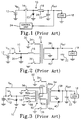
- Many regulator topologies have been proposed in the past, including the basic forward converter or "buck" regulator 10 illustrated in FIG. 1.
- An unregulated D.C. voltage V IN from a battery 12 is applied through a switch 14 and energy storage inductor 16 to a load 18.
- the cathode of a diode 20 is connected to the junction of the switch 14 and inductor 16, with the anode of the diode 20 being connected to ground.
- a smoothing capacitor 22 is connected across the load 18.
- a control unit 24 periodically closes and opens the switch 14 to "chop" the input voltage V IN applied to the inductor 16.
- the inductor 16 and diode 20 constitute a "flywheel" arrangement which causes current to flow continuously from the inductor 16 into the load 18 in the direction of the arrow 26.
- the load 18 dissipates current continuously, regardless of whether the switch 14 is open or closed.
- the capacitor 22 charges to the time averaged value of voltage across the load 18, providing a smoothed or regulated D.C. output voltage V OUT .
- the output voltage V OUT can be regulated by varying the duty cycle (proportion of time the switch 14 is closed during each cycle) of the switch 14. This operation is known in the art as pulse width modulation (PWM).
- PWM pulse width modulation
- the output voltage V OUT will approach V IN as the duty cycle is increased toward 100%, and will approach zero as the duty cycle approaches 0%.
- Regulation of the output voltage V OUT to a predetermined value is accomplished by sensing the actual value of V OUT , increasing the duty cycle if V OUT drops below the predetermined value, and decreasing the duty cycle if V OUT increases above the predetermined value. In this configuration, the output voltage V OUT cannot exceed the input voltage V IN .
- the regulator 10 is disadvantageous in that the inductor 16 must accommodate the entire current flow through the load 18, and must necessarily be large and heavy. This is unacceptable in applications where space and weight must be strictly conserved.
- the regulator 10 also suffers from inefficiency since the entire load current flows through the diode 20 when the switch 14 is open.
- the diode 20 introduces a voltage drop of approximately one volt into the circuit, which dissipates power equal to the voltage drop multiplied by the current flow.
- the dissipative power loss is inversely proportional to the output voltage, and can become excessive in low voltage applications.
- FIG. 2 illustrates a regulator 30 including the buck regulator of FIG. 1 combined with a "chopper" in a "push-pull", or more accurately a "push-push” arrangement.
- the inductor 16 is connected to the center tap of a primary winding of a transformer 32, with the opposite ends of the primary winding being connected through chopper switches 34 and 36 to ground.
- the center tap of a secondary winding of the transformer 32 is grounded, with the opposite ends of the secondary winding being connected to the anodes of rectifier diodes 38 and 40.
- the cathodes of the diodes 38 and 40 are connected together across the capacitor 22 and load 18.
- the switches 34 and 36 constitute a chopper, and are alternatively driven with typically 50% duty cycle. More specifically, the switch 34 is closed when the switch 36 is open and vice-versa. This causes current to be induced in the secondary winding of the transformer 32 in alternating directions, which is rectified and converted to pulsating D.C. by the diodes 38 and 40. The pulsating D.C. is converted to smoothed D.C. by the capacitor 22.
- the regulator 32 is capable of producing an output voltage V OUT which is higher than the input voltage V IN due to the provision of the transformer 32.
- V OUT the entire load current must still flow through the inductor 16 and diode 20, and there are two switches in the input current path as opposed to one switch in the basic regulator 10.
- the switches 14, 34 and 36 are embodied as switching transistors, which introduce voltage drops into the circuit in a manner similar to diodes. This can result in excessive power loss at low input voltages.
- Most prior art converters have been unable to achieve efficiencies in excess of 88%.
- FIG. 3 illustrates a regulator 50 which is disclosed in U.S. patent no. 4,943,903, entitled "POWER SUPPLY IN WHICH REGULATION IS ACHIEVED BY PROCESSING A SMALL PORTION OF APPLIED POWER THROUGH A SWITCHING REGULATOR", issued July 24, 1990 to Gilbert I. Cardwell, Jr., who is also one of the present inventors.
- a first transformer 52 has a center-tapped primary winding including two sections 52a and 52b and a center-tapped secondary winding having two sections 52c and 52d.
- the center tap of the primary winding sections 52a and 52b is connected to the inductor 16, whereas the opposite ends of the sections 52a and 52b are connected through switches 56 and 58 respectively to ground.
- the center tap of the secondary winding sections 52c and 52d is connected to the battery 12.
- a second transformer 54 has two primary windings 54a and 54b and a center tapped secondary winding which is connected to the diodes 38 and 40 in the same manner as in the regulator 30.
- One end of the winding 52a is connected to ground through the switch 34, whereas one end of the winding 52b is connected to ground through the switch 36.
- the opposite ends of the windings 54a and 54b are connected to the opposite ends of the windings 52a and 52b respectively.
- the switches 34,56 are driven alternatingly with the switches 36,58 at typically 50% duty cycle.
- the switch 14 is driven as described above with a variable duty cycle to regulate the output voltage V OUT . This is accomplished by producing a voltage at the center tap of the first transformer 52 which increases as the duty cycle of the switch 14 increases.
- Closing of the switch 34 or 36 causes voltage V IN to be applied across the series combination of windings 54a,52c or 54b,52d respectively. If the switch 14 is driven with 0% duty cycle, the voltage at the center tap of the primary winding sections 52a and 52b will be zero, and the voltage across the sections 52a and 52b will also be zero. Due to transformer action, the voltage across the secondary winding sections 52c and 52d will also be zero. The voltage across the windings 54a or 54b will be equal to V IN . Assuming that the turns ratio of the transformer 54 is unity, V OUT will be equal to V IN .
- the voltage at the center tap of the primary winding sections 52a and 52b will be substantially equal to V IN . Due to transformer action, a voltage will be induced across the winding sections 52c and 52d equal to V IN divided by the turns ratio of the transformer 52. Assuming an exemplary turns ratio of 5:1, the induced voltage across the winding sections 52c and 52d will be V IN /5.
- the voltage appearing across the primary winding section 54a or 54b is thereby equal to V IN (from the battery 12) plus V IN /5 (from the winding section 52c or 52d) or 1.2 x V IN .
- the transformer 52 adds a fraction of the voltage produced by the buck regulator 10, which is continuously variable and increases as the duty cycle of the switch 14 increases, to the input voltage V IN .
- the regulator 50 is advantageous over the regulator 30 in that the main portion of the input current flows through the windings 54a,52c or 54b,52d which are inductive elements and not subject to dissipative loss.
- the input current flows through only one switch 34 or 36 in the main current path. Only a fraction of the input current (in this case a maximum of 17%) flows through the auxiliary or regulating current path including the regulator 10 and is thereby subject to dissipative losses as described above.
- the regulator 50 is only capable of unilateral regulation. In other words, it is capable of adding a regulating voltage to the input voltage, but not subtracting a regulating voltage therefrom.
- the turns ratio of the transformer 52 is selected such that the switch 14 will be driven at 50% duty cycle and the regulating voltage appearing across the winding section 52c or 52d will be one-half the maximum regulating voltage when the input and output voltages V IN and V OUT are at their predetermined (nominal, average or center of range) design values.
- the turns ratio of the transformer 54 is selected such that, with the predetermined design value of V IN plus one-half the maximum regulating voltage applied across the winding section 54a or 54b, the predetermined design value of V OUT will appear across the load 18. In other words, when V IN and V OUT are at the center of their ranges, the regulating voltage will be at the center of its range.
- This design is able to achieve efficiencies of 95%, but only if the system has a small input voltage range (e.g. ⁇ 5%).
- an unregulated D.C. input voltage is processed by a high power chopper to produce a first chopped signal having the same voltage as the input, and by a low power chopper to produce a second or regulating chopped signal in synchronism with and having a lower voltage than the first chopped signal.
- the first and second chopped signals are algebraically combined by transformers to produce an A.C. output signal which may be converted to D.C.
- the second chopped signal may be controlled to have the same polarity relative to the first chopped signal in which case the voltages add to increase the output voltage, or to have the opposite polarity relative to the first chopped signal in which case the voltages subtract to decrease the output voltage.
- the second chopped signal will normally be controlled to add part of the time and subtract for the remainder of the time. In this way, the power converter can change the ratio of input voltage to output voltage over a wide range.
- An energy storage inductor is provided in the high power chopper path to average the voltage addition and subtraction.
- the high power chopper operation may be intermittently interrupted to limit input current flow during startup, and switches are provided in the embodiment of FIG. 7 to allow interruption without causing dangerous voltage surges.
- the added switches of FIG. 7 discharge energy stored in the inductor into the output transformer and thereby contribute to the output voltage.
- the present regulator improves over the prior art regulator illustrated in FIG. 3 in that the energy storage inductor can be smaller than in the prior art regulator for the same regulation range. This is because the present regulator provides bilateral regulation (both addition and subtraction modes), and thereby twice the range of regulation as the prior art regulator using corresponding circuit elements.
- the turns ratio of the transformer which produces the regulating voltage may also be one-half that of the corresponding transformer in the prior art regulator, since twice the regulating range can be obtained with the same turns ratio in accordance with the present invention. This enables the size and weight of the transformer to be reduced over the prior art, or the designer may chose to use the same size and weight and achieve wider regulating range.
- FIG. 4 A D.C. chopper voltage regulator or converter embodying the present invention is illustrated in FIG. 4 and generally designated as 60.
- the present regulator 60 is a direct improvement over the prior art regulator 50 illustrated in FIG. 3.
- like elements are designated in FIG. 4 by the same reference numerals used in FIG. 3. It will be understood, however, that the manner in which the elements are interconnected in accordance with the present invention causes the regulator 60 to operate in a fundamentally different manner than the regulator 50.
- the buck regulator 10 is omitted, and the battery 12 is connected directly to the center tap of the primary winding sections 52a and 52b of the first transformer 52.
- An energy storage inductor 62 is connected between the battery 12 and the center tap of the secondary winding sections 52c and 52d of the transformer 52.
- the inductor 16 of the prior art regulator 50 is part of the buck regulator 10 thereof, and is not included in the regulator 60.
- the inductor 62 of the present regulator 60 does not have a corresponding circuit element in the prior art regulator 50.
- the switches 34, 36, 56 and 58 are controlled by a control unit 64 which senses the output voltage V OUT , input voltage V IN , output current and/or input current, compares the sensed parameter with a command voltage V C or other command value and controls regulation in accordance therewith.
- the output voltage V OUT is able to vary in response to variations in the command voltage V C .
- the output voltage V OUT iS compared to the command voltage V C for regulation.
- the output voltage V OUT is desired to be constant in the presence of a varying input voltage V IN .
- the output voltage is compared to a reference voltage.
- the output current may be the controlling parameter which is to be regulated and the control law built into the control unit can accommodate these variations.
- the switches 34 and 36 are typically driven alternatingly with 50% duty cycle, and constitute a first chopper which periodically interrupts the input voltage V IN to produce a first chopped signal in the form of a square wave across the series combination of the winding sections 54a or 54b, 52c or 52d and inductor 62.
- the switches 56 and 58 are driven in synchronism (like frequency, variable phase) with the switches 34 and 36, and constitute a second chopper which periodically interrupts the input voltage V IN to produce a second chopped signal in the form of a square wave across the primary winding section 52a or 52b respectively.
- the second chopped signal is transformed by the transformer 52 and appears across the winding section 52c or 52d as a third chopped signal which is also in synchronism with the first chopped signal, but has a smaller voltage and a polarity which can be the same or opposite relative to the polarity of the first chopped signal.
- a simplified manner of viewing the second chopper is to disregard the signals across the primary winding sections 52a or 52b, and consider the switches 56 and 58 in combination with the transformer 52 as producing a second chopped signal across the winding section 52c or 52d.
- the second chopped signal corresponds to the third chopped signal described above.
- the signal chopped by the switches 34 and 36 constitutes a main power signal for supply to the load 18.
- the signal chopped by the switches 56 and 58 constitutes a relatively low power regulating signal, and is algebraically combined with the main power signal by the transformer 52 to provide the regulated output voltage V OUT .
- the polarities of the winding sections of the transformers 52 and 54 are indicated by the dot winding convention.
- the "opposite end" of a winding section is construed to mean the end of the winding section opposite the dot end thereof.
- the regulator 60 is operated in an addition mode by closing the switches 34,58 or 36,56 together, or in a subtraction mode by closing the switches 34,56 or 36,58 together. The operation will be described for the four possible cases as follows.
- the center tap of the sections 52a and 52b receives V IN from the battery 12.
- the dot end of the section 52b is negative relative to the opposite end.
- Due to the action of the transformer 52 the dot end of the secondary winding section 52c is negative relative to the opposite end thereof.
- a voltage is induced in the section 52c having a value equal to V IN divided by the turns ratio of the transformer 52. Assuming an exemplary turns ratio of 5:1, the voltage induced in the section 52c will be V IN /5. This voltage has the same polarity as V IN .
- the voltage applied to the primary winding section 54a of the transformer 54 is equal to V IN (from the battery 12) plus V IN /5 (across the secondary winding section 52c) or 1.2 x V IN minus the voltage across the inductor 62.
- the voltage across the inductor 62 causes the inductor current to increase.
- the switch 56 connects the opposite end of the section 52a to ground.
- the center tap of the sections 52a and 52b receives V IN from the battery 12.
- the dot end of the section 52a is positive relative to the opposite end.
- Due to the action of the transformer 52 the dot end of the secondary winding section 52c is positive relative to the opposite end thereof. The result is that a voltage is induced in the section 52c having a value equal to V IN /5, and the opposite polarity relative to V IN .
- the voltage applied to the primary winding section 54a of the transformer 54 is equal to V IN (from the battery 12) minus V IN /5 (across the section 52c) or 0.8 x V IN plus the voltage across the inductor 62.
- the voltage across the inductor causes the inductor current to decrease.
- the center tap of the sections 52a and 52b receives V IN from the battery 12.
- the dot end of the section 52a is positive relative to the opposite end.
- the opposite end of the secondary winding section 52d is clamped negative relative to the dot end thereof.
- a voltage is induced in the section 52d having a value equal to V IN /5, and the same polarity as V IN .
- the voltage applied to the primary winding section 54b of the transformer 54 is equal to 1.2 x V IN minus the voltage across the inductor 62.
- the voltage across the inductor 62 causes the inductor current to increase in the same manner as in Case I.
- the center tap of the sections 52a and 52b receives V IN from the battery 12.
- the dot end of the section 52b is negative relative to the opposite end.
- Due to the action of the transformer 52 the dot end of the secondary winding section 52d is clamped negative relative to the opposite end thereof.
- a voltage is induced in the section 52d having a value equal to V IN /5, and the opposite polarity relative to V IN .
- the voltage applied to the primary winding section 54b of the transformer 54 is equal 0.8 x V IN plus the voltage across the inductor 62.
- the voltage across the inductor 62 causes the inductor current to decrease, similar to Case II.
- the switches 34 and 36 are alternatingly driven with 50% duty cycle.
- the switch 58 is closed and the switch 56 opened to produce addition mode (Case I), and subsequently the switch 56 is closed and the switch 58 opened to produce subtraction mode (Case II).
- Voltage regulation is performed by varying the relative duty cycles of the addition and subtraction modes.
- the control unit 64 causes the switch 58 (addition mode) to be closed for a relatively longer time than the switch 56 (subtraction mode), such that the regulator 60 operates in addition mode longer than in subtraction mode and the output voltage V OUT increases.
- the duty cycle is increased as the amount of deviation of the sensed voltage from the predetermined design voltage increases to provide a higher correction for larger amounts of deviation.
- the control unit 64 causes the switch 58 (addition mode) to be closed for a relatively shorter time than the switch 56 (subtraction mode), such that the regulator 60 operates in subtraction mode longer than in addition mode.
- the operation is essentially similar during the times the switch 36 is closed, with the switch 56 being closed for addition mode (Case III) and the switch 58 being closed for subtraction mode (Case IV).
- the voltage induced across the secondary winding of the transformer 54 is A.C.
- the diodes 38 and 40 and capacitor 22 are omitted and the output voltage is constituted by this A.C. voltage.
- the diodes 38 and 40 rectify the A.C. voltage to produce a pulsating D.C. voltage, which is smoothed by the capacitor 22 to produce the smooth D.C. output voltage V OUT .
- FIG. 4 further illustrates how switches 66 and 68 may be provided to enable alternative methods of driving the regulator 60.
- the switches 66 and 68 are connected across the winding sections 52a and 52b respectively, and controlled by the control unit 64 in a desired manner.
- the switch 66 and/or 68 can be closed to short out one or both of the sections 52a and 52b and enable a mode of operation in which neither addition nor subtraction occurs.
- the inductor loss terms are halved when this option can be used. It is further possible to open both switches 56 and 58 simultaneously to completely open the primary winding sections 52a and 52b.
- FIG. 5 illustrates a regulator 70 in which the switches 34, 36, 56 and 58 are replaced by NPN bipolar transistors 72, 74, 76 and 78 respectively. Diodes 80 and 82 are connected across the emitter and collector of the transistors 76 and 78 respectively in anti-parallel relation. This arrangement simplifies the control of the switches since it is necessary to close only switch 72 or 74 to produce a subtraction mode.
- bipolar transistors 76 and 78 can be replaced by metal-oxide-semiconductor field-effect transistors (MOSFETs) which inherently include anti-parallel diodes, in which case the diodes 80 and 82 can be omitted.
- MOSFETs metal-oxide-semiconductor field-effect transistors
- the operation of the regulator 70 will be described with reference also being made to the timing diagram of FIG. 6.
- the drive signals applied by a control unit 90 to the bases of the transistors 72, 74, 76 and 78 are designated as D72, D74, D76 and D78 respectively.
- the voltages at the collectors of the transistors 72, 74, 76 and 78 are designated as V72, V74, V76 and V78 respectively. Further illustrated are the voltage V84 at the center tap 84 of the secondary winding of the transformer 52, the current I62 through the inductor 62, the current I86 through the center tap 86 of the primary winding of the transformer 52, the current I88 flowing out of the battery 12 and the current I76 flowing through the collector of the transistor 76.
- the transistors 72 and 78 are turned on. Current induced from the secondary winding section 52c into the primary winding section 52b flows out of the dot end of the section 52b through the transistor 78 to ground. The dot end of the section 52b is connected to ground, causing a voltage with the same polarity as V IN to be induced in the section 52c. This operation is equivalent to closing the switches 34 and 58 of the regulator 60.
- Subtraction mode is produced by turning on only the transistor 72.
- a voltage is induced across the section 52a such that the dot end is positive relative to the opposite end.
- Increasing current flow through the section 52c causes the induced voltage in the section 52a to increase until the opposite end of the section 52a is one diode drop more negative than ground. This forward biases the diode 80, enabling current induced from the section 52c to flow from ground through the diode 80 and section 52a into the battery 12.
- the opposite end of the section 52a is effectively connected to ground through the diode 80, causing a voltage with the dot having the same polarity as V IN to be induced in the section 52c.
- This operation is equivalent to closing the switches 34 and 56 of the regulator 60, with the diode 80 performing the function of the switch 56.
- the transistors 74 and 76 are turned on. Current induced from the secondary winding section 52d into the primary winding section 52a flows from out of the opposite end of the winding 52a through the transistor 76 to ground. The opposite end of the section 52a is connected to ground, causing a voltage with the same polarity as V IN to be induced in the section 52d. This operation is equivalent to closing the switches 36 and 56 of the regulator 60.
- Subtraction mode is produced by turning on only the transistor 74.
- a voltage is induced across the section 52b such that the dot end is negative relative to the opposite end.
- Increasing current flow through the section 52d causes the induced voltage to increase until the opposite end of the section 52b is one diode drop more negative than ground. This forward biases the diode 82, enabling current induced from the section 52d to flow from ground through the diode 82 and section 52b into the battery 12.
- the dot end of the section 52b is effectively connected to ground through the diode 82, causing a voltage with the opposite polarity relative to V IN to be induced in the section 52d.
- This operation is equivalent to closing the switches 36 and 58 of the regulator 60, with the diode 82 performing the function of the switch 58.
- the collector voltages of the transistors 76 and 78 vary only slightly between the addition and subtraction modes. In addition mode the voltage is ground, whereas in subtraction mode the voltage is one diode drop (approximately one volt) negative of ground. This small difference eliminates one term of switching loss in the regulator 70.
- the present regulator 60 improves over the prior art regulator 50 in that the energy storage inductor 62 need only be half as large as the inductor 16 in the regulator 50. This is because the present regulator 60 provides bilateral regulation (both addition and subtraction modes), and thereby twice the range of regulation as the regulator 50 using corresponding circuit elements.
- the smaller and lighter inductor 62 enables the regulator 60 to be used in applications in which size and weight constraints would preclude the use of the regulator 50.
- the turns ratio of the transformer 52 which produces the regulating voltage may also be one-half that of the corresponding transformer in the regulator 50, since twice the regulating range can be obtained with the same turns ratio in accordance with the present invention. This enables the size and weight of the transformer 52 to be reduced over the prior art.
- the present regulator 60 also eliminates the buck regulator 10 including the diode 20 which is an inherent element in the prior art regulator 50, thereby eliminating the dissipative loss associated therewith.
- a problem inherent in the basic regulator 60 or 70 is that it is difficult to control the initial supply of input voltage V IN .
- V IN input voltage
- the entire input voltage V IN is effectively applied across the inductor 16 and primary winding sections 54a and 54b which could cause the input current to rapidly increase to a level high enough to destroy the switches 34 and 36.
- the switches 34 and 36 must both be opened before this occurs in order to limit the input current.
- the back EMF in the inductor 62 is then applied across the switches 34 and 36 which is also high enough to cause severe damage.
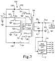
- FIG. 7 illustrates a regulator 100 in which additional elements are added to the basic regulator 60 to prevent excessive current flow during startup.
- Switches 102 and 104 are connected between the junction of 54a,34 and the battery 12, and between the junction of 54b,36 and the battery 12 respectively.
- Diodes 106 and 108 are connected in series with the switches 102 and 104 respectively, with the cathodes of the diodes 106 and 108 being connected to the battery 12.
- a startup control unit 110 is additionally provided which cooperates with the control unit 64 to control the switches 102 and 104.
- the switches 34, 36, 56 and 58 are alternatingly controlled to operate exclusively in subtraction mode to reduce the input current flow.
- the switches 34, 36, 56 and 58 are closed for a length of time which is insufficient for the input current to increase to an excessive level.
- the diodes 106 and 108 are reverse biased during this operation, preventing current from flowing through the switches 102 and 104.
- the switches 34, 36, 56 and 58 are then opened and the one of the switches 102 and 104 is closed. Assuming that the switch 102 is closed, the back EMF of the inductor 62 will cause current flow through the sections 52c and 54a, switch 102 and diode 106 in the same direction as the input current. This current is induced into the secondary winding of the transformer 54 and supplied to the load 18. Power dissipation by the load 18 reduces the current flow to a level low enough that the switches 34, 36, 38 and 40 can be closed again to supply more energy into the regulator 100 and increase the output voltage V OUT toward the predetermined design level. The operation is essentially similar with the switch 104 closed.
- the operation of the switches 34, 36, 56 and 58 alternates with the operation of the switches 102 and 104 to supply a safe incremental amount of energy into the inductor 62, and then discharge energy from the inductor 62 into the load 18.
- the timing of closing and opening the switches 102 and 104 is variable over a large range. Typically, the switch 102 will be closed when the switch 34 is opened, and the switch 104 will be closed with the switch 36 is opened.
- Fig. 7 The arrangement of Fig. 7 is desirable in that substantially no power is dissipated in the regulator 100 during startup. All of the input power (excluding low order losses) is either supplied directly to the load 18, or stored in the inductor 62 and subsequently supplied therefrom to the load 18.
- An unregulated D.C. input voltage V IN is processed by a high power chopper 34,36 to produce a first chopped signal having the same voltage as the input voltage V IN , and by a low power chopper 56,58 to produce a second chopped signal in synchronism with and having a lower voltage than the first chopped signal.
- the first and second chopped signals are algebraically combined by transformers 52,54 to produce an A.C. output signal which may be converted to D.C. V OUT .
- the second chopped signal may be controlled to have the same polarity relative to the first chopped signal in which case the voltages add to increase the output voltage V OUT , or to have the opposite polarity relative to the first chopped signal in which case the voltages substract to decrease the output voltage V OUT .
- the periods of addition and subtraction are alternated within the period of the first chopped signal.
- the ratio of addition and subtraction of the second chopped signal may be varied to adjust the ratio of output voltage to input voltage over a wide range.
- An energy storage inductor 62 is provided in the high power chopper path to average the voltage addition and subtraction.
- the high power chopper operation may be intermittently interrupted to limit input current flow during startup, and switches 102,104 are provided to discharge energy stored in the inductor 62 into the transformers 52,54 and thereby contribute to the output voltage V OUT .
Landscapes
- Engineering & Computer Science (AREA)
- Power Engineering (AREA)
- Dc-Dc Converters (AREA)
- Rectifiers (AREA)
Applications Claiming Priority (2)
| Application Number | Priority Date | Filing Date | Title |
|---|---|---|---|
| US07/845,074 US5218522A (en) | 1992-03-03 | 1992-03-03 | D.C. chopper regulating method and apparatus incorporating bilateral regulating voltage path |
| US845074 | 1992-03-03 |
Publications (2)
| Publication Number | Publication Date |
|---|---|
| EP0559009A1 true EP0559009A1 (fr) | 1993-09-08 |
| EP0559009B1 EP0559009B1 (fr) | 1995-12-20 |
Family
ID=25294336
Family Applications (1)
| Application Number | Title | Priority Date | Filing Date |
|---|---|---|---|
| EP93102521A Expired - Lifetime EP0559009B1 (fr) | 1992-03-03 | 1993-02-18 | Méthode de régulation pour hacheur de courant continu et dispositif incorporant un contrÔleur bilateral de tension |
Country Status (5)
| Country | Link |
|---|---|
| US (1) | US5218522A (fr) |
| EP (1) | EP0559009B1 (fr) |
| JP (1) | JP3369621B2 (fr) |
| CA (1) | CA2087566A1 (fr) |
| DE (1) | DE69301040T2 (fr) |
Cited By (1)
| Publication number | Priority date | Publication date | Assignee | Title |
|---|---|---|---|---|
| EP1160962A3 (fr) * | 2000-06-01 | 2003-04-02 | The Boeing Company | Convertisseur additioneur/soustracteur courant continu - courant continu avec trois commutateurs |
Families Citing this family (24)
| Publication number | Priority date | Publication date | Assignee | Title |
|---|---|---|---|---|
| US5517400A (en) * | 1992-02-03 | 1996-05-14 | Ulrich Schwan | Method for synchronizing converters of an inductive element for reversible energy transmission |
| GB9206020D0 (en) * | 1992-03-19 | 1992-04-29 | Astec Int Ltd | Transition resonant convertor |
| US5327337A (en) * | 1992-09-01 | 1994-07-05 | Broadcast Electronics, Inc. | Resonant push-pull switching power amplifier |
| US5295058A (en) * | 1992-10-13 | 1994-03-15 | Recoton Corporation | Universal DC to DC power converter |
| DE4328556C2 (de) * | 1993-08-25 | 1995-06-08 | Ant Nachrichtentech | Gegentaktwandler mit Vorregler |
| JP2767781B2 (ja) * | 1993-09-17 | 1998-06-18 | 東光株式会社 | Ac−dcコンバータ |
| JPH0795774A (ja) * | 1993-09-20 | 1995-04-07 | Asia Denshi Kogyo Kk | 低ノイズコンバータ |
| FR2713030B1 (fr) * | 1993-11-24 | 1996-01-12 | Merlin Gerin | Alimentation sans coupure à neutre traversant, comportant un hacheur-élévateur double. |
| US6297724B1 (en) | 1994-09-09 | 2001-10-02 | The Whitaker Corporation | Lighting control subsystem for use in system architecture for automated building |
| US5907482A (en) * | 1995-11-30 | 1999-05-25 | Toko, Inc. | Power supply control device |
| EP0954899A2 (fr) | 1997-01-24 | 1999-11-10 | Fische, LLC | Convertisseur de puissance a haute efficacite |
| US7269034B2 (en) | 1997-01-24 | 2007-09-11 | Synqor, Inc. | High efficiency power converter |
| US6055162A (en) * | 1998-03-12 | 2000-04-25 | Northrop Grumman Corporation | Self-oscillating DC-DC converter apparatus and method especially adaptable for VHF operation |
| US5969955A (en) * | 1998-12-29 | 1999-10-19 | General Electric Company | Push-pull power converter with crowbar circuit for very fast output voltage turn-off |
| DE19943575A1 (de) * | 1999-09-13 | 2001-03-22 | Mannesmann Vdo Ag | Gleichspannungswandler |
| US6836414B1 (en) | 2002-10-17 | 2004-12-28 | University Of Central Florida | PWM half-bridge converter with dual-equally adjustable control signal dead-time |
| US6806662B1 (en) * | 2003-05-28 | 2004-10-19 | The Boeing Company | Multiple mode universal power source utilizing a rotating machine |
| US7339809B2 (en) * | 2004-11-30 | 2008-03-04 | The Boeing Company | Systems and methods for electrical power regulation and distribution in aircraft |
| US20070002593A1 (en) * | 2005-06-30 | 2007-01-04 | Dinh James S | Isolated DCX converter |
| JP2008138820A (ja) | 2006-12-05 | 2008-06-19 | Toyota Motor Corp | ベルト式無段変速機の油圧制御装置 |
| US7859870B1 (en) * | 2008-07-29 | 2010-12-28 | Lockheed Martin Corporation | Voltage clamps for energy snubbing |
| TWI435536B (zh) * | 2010-11-18 | 2014-04-21 | Univ Nat Formosa | 低雜訊的交流截波電路 |
| US10199950B1 (en) | 2013-07-02 | 2019-02-05 | Vlt, Inc. | Power distribution architecture with series-connected bus converter |
| CA3069966A1 (fr) * | 2017-07-14 | 2019-01-17 | Alpha Technologies Services, Inc. | Systemes et procedes d'alimentation en courant alternatif a regulation de tension |
Citations (3)
| Publication number | Priority date | Publication date | Assignee | Title |
|---|---|---|---|---|
| GB2123225A (en) * | 1982-06-14 | 1984-01-25 | Chiyoda Kk | Pulse power source device |
| EP0137055A1 (fr) * | 1983-09-15 | 1985-04-17 | Ibm Deutschland Gmbh | Dispositif d'alimentation à découpage avec protection contre la surintensité |
| US4943903A (en) * | 1989-03-14 | 1990-07-24 | Cardwell Jr Gilbert I | Power supply in which regulation is achieved by processing a small portion of applied power through a switching regulator |
Family Cites Families (1)
| Publication number | Priority date | Publication date | Assignee | Title |
|---|---|---|---|---|
| US4698742A (en) * | 1986-08-01 | 1987-10-06 | The United States Of America As Represented By The Secretary Of The Air Force | High-voltage milberger slip slide power conditioner |
-
1992
- 1992-03-03 US US07/845,074 patent/US5218522A/en not_active Expired - Lifetime
-
1993
- 1993-01-19 CA CA002087566A patent/CA2087566A1/fr not_active Abandoned
- 1993-02-18 DE DE69301040T patent/DE69301040T2/de not_active Expired - Lifetime
- 1993-02-18 EP EP93102521A patent/EP0559009B1/fr not_active Expired - Lifetime
- 1993-03-03 JP JP04290593A patent/JP3369621B2/ja not_active Expired - Fee Related
Patent Citations (3)
| Publication number | Priority date | Publication date | Assignee | Title |
|---|---|---|---|---|
| GB2123225A (en) * | 1982-06-14 | 1984-01-25 | Chiyoda Kk | Pulse power source device |
| EP0137055A1 (fr) * | 1983-09-15 | 1985-04-17 | Ibm Deutschland Gmbh | Dispositif d'alimentation à découpage avec protection contre la surintensité |
| US4943903A (en) * | 1989-03-14 | 1990-07-24 | Cardwell Jr Gilbert I | Power supply in which regulation is achieved by processing a small portion of applied power through a switching regulator |
Cited By (1)
| Publication number | Priority date | Publication date | Assignee | Title |
|---|---|---|---|---|
| EP1160962A3 (fr) * | 2000-06-01 | 2003-04-02 | The Boeing Company | Convertisseur additioneur/soustracteur courant continu - courant continu avec trois commutateurs |
Also Published As
| Publication number | Publication date |
|---|---|
| JP3369621B2 (ja) | 2003-01-20 |
| CA2087566A1 (fr) | 1993-09-04 |
| DE69301040T2 (de) | 1996-07-25 |
| JPH066974A (ja) | 1994-01-14 |
| EP0559009B1 (fr) | 1995-12-20 |
| DE69301040D1 (de) | 1996-02-01 |
| US5218522A (en) | 1993-06-08 |
Similar Documents
| Publication | Publication Date | Title |
|---|---|---|
| EP0559009B1 (fr) | Méthode de régulation pour hacheur de courant continu et dispositif incorporant un contrÔleur bilateral de tension | |
| US4559590A (en) | Regulated DC to DC converter | |
| US6664762B2 (en) | High voltage battery charger | |
| US6115267A (en) | AC-DC converter with no input rectifiers and power factor correction | |
| EP0571067B1 (fr) | Convertisseur du type "forward" avec deux commutateurs actifs et aptitude à facteur de puissance unité | |
| US7339287B2 (en) | Power converter | |
| US5291383A (en) | Simplified UPS system | |
| US6538909B2 (en) | Universal high efficiency power converter | |
| EP0262812B1 (fr) | Convertisseur résonant parallèle élévateur-abaisseur | |
| US6583999B1 (en) | Low output voltage, high current, half-bridge, series-resonant, multiphase, DC-DC power supply | |
| US7272021B2 (en) | Power converter with isolated and regulated stages | |
| US6344768B1 (en) | Full-bridge DC-to-DC converter having an unipolar gate drive | |
| US6549432B1 (en) | Single-winding, multiple-output, bi-directional flyback converter | |
| EP1813012B1 (fr) | Convertisseur ca-cc | |
| US5734237A (en) | Integrated DC electric controller/charger | |
| US5225767A (en) | Synchronous switching power supply with boost and/or flyback converters | |
| US7050309B2 (en) | Power converter with output inductance | |
| US5221887A (en) | Synchronous switching power supply comprising boost or flyback converter | |
| KR20020024444A (ko) | 고효율의 스위칭모드 전원공급기 | |
| KR200216665Y1 (ko) | 고효율의 스위칭모드 전원공급기 | |
| JP2795229B2 (ja) | Dc−dcコンバータ | |
| JPH0326796Y2 (fr) | ||
| JP3221899B2 (ja) | スイッチングレギュレータ | |
| JPH04121055A (ja) | 直流電流検出回路およびdc―dcコンバータ | |
| IE20050719A1 (en) | An ACDC converter |
Legal Events
| Date | Code | Title | Description |
|---|---|---|---|
| PUAI | Public reference made under article 153(3) epc to a published international application that has entered the european phase |
Free format text: ORIGINAL CODE: 0009012 |
|
| AK | Designated contracting states |
Kind code of ref document: A1 Designated state(s): DE FR GB IT |
|
| 17P | Request for examination filed |
Effective date: 19940302 |
|
| 17Q | First examination report despatched |
Effective date: 19940614 |
|
| GRAA | (expected) grant |
Free format text: ORIGINAL CODE: 0009210 |
|
| AK | Designated contracting states |
Kind code of ref document: B1 Designated state(s): DE FR GB IT |
|
| ITF | It: translation for a ep patent filed | ||
| REF | Corresponds to: |
Ref document number: 69301040 Country of ref document: DE Date of ref document: 19960201 |
|
| ET | Fr: translation filed | ||
| PLBQ | Unpublished change to opponent data |
Free format text: ORIGINAL CODE: EPIDOS OPPO |
|
| PLBI | Opposition filed |
Free format text: ORIGINAL CODE: 0009260 |
|
| PLBF | Reply of patent proprietor to notice(s) of opposition |
Free format text: ORIGINAL CODE: EPIDOS OBSO |
|
| 26 | Opposition filed |
Opponent name: AGENCE SPATIALE EUROPEENNE Effective date: 19960918 |
|
| PG25 | Lapsed in a contracting state [announced via postgrant information from national office to epo] |
Ref country code: GB Effective date: 19970218 |
|
| PLBF | Reply of patent proprietor to notice(s) of opposition |
Free format text: ORIGINAL CODE: EPIDOS OBSO |
|
| GBPC | Gb: european patent ceased through non-payment of renewal fee |
Effective date: 19970218 |
|
| PLBO | Opposition rejected |
Free format text: ORIGINAL CODE: EPIDOS REJO |
|
| PLBN | Opposition rejected |
Free format text: ORIGINAL CODE: 0009273 |
|
| STAA | Information on the status of an ep patent application or granted ep patent |
Free format text: STATUS: OPPOSITION REJECTED |
|
| 27O | Opposition rejected |
Effective date: 19980810 |
|
| REG | Reference to a national code |
Ref country code: FR Ref legal event code: TP Ref country code: FR Ref legal event code: CD Ref country code: FR Ref legal event code: CA |
|
| REG | Reference to a national code |
Ref country code: FR Ref legal event code: TP Ref country code: FR Ref legal event code: CD |
|
| PGFP | Annual fee paid to national office [announced via postgrant information from national office to epo] |
Ref country code: FR Payment date: 20120306 Year of fee payment: 20 |
|
| PGFP | Annual fee paid to national office [announced via postgrant information from national office to epo] |
Ref country code: DE Payment date: 20120228 Year of fee payment: 20 |
|
| PGFP | Annual fee paid to national office [announced via postgrant information from national office to epo] |
Ref country code: IT Payment date: 20120224 Year of fee payment: 20 |
|
| REG | Reference to a national code |
Ref country code: DE Ref legal event code: R071 Ref document number: 69301040 Country of ref document: DE |
|
| REG | Reference to a national code |
Ref country code: DE Ref legal event code: R071 Ref document number: 69301040 Country of ref document: DE |
|
| PG25 | Lapsed in a contracting state [announced via postgrant information from national office to epo] |
Ref country code: DE Free format text: LAPSE BECAUSE OF EXPIRATION OF PROTECTION Effective date: 20130219 |