EP0562273A2 - Verfahren zur Verbesserung der Eigenschaften der Grenzfläche CaF2 auf Silizium - Google Patents
Verfahren zur Verbesserung der Eigenschaften der Grenzfläche CaF2 auf Silizium Download PDFInfo
- Publication number
- EP0562273A2 EP0562273A2 EP93102540A EP93102540A EP0562273A2 EP 0562273 A2 EP0562273 A2 EP 0562273A2 EP 93102540 A EP93102540 A EP 93102540A EP 93102540 A EP93102540 A EP 93102540A EP 0562273 A2 EP0562273 A2 EP 0562273A2
- Authority
- EP
- European Patent Office
- Prior art keywords
- caf2
- temperature
- silicon surface
- maintaining
- annealing
- Prior art date
- Legal status (The legal status is an assumption and is not a legal conclusion. Google has not performed a legal analysis and makes no representation as to the accuracy of the status listed.)
- Granted
Links
Images

Classifications
-
- H—ELECTRICITY
- H10—SEMICONDUCTOR DEVICES; ELECTRIC SOLID-STATE DEVICES NOT OTHERWISE PROVIDED FOR
- H10P—GENERIC PROCESSES OR APPARATUS FOR THE MANUFACTURE OR TREATMENT OF DEVICES COVERED BY CLASS H10
- H10P14/00—Formation of materials, e.g. in the shape of layers or pillars
- H10P14/60—Formation of materials, e.g. in the shape of layers or pillars of insulating materials
- H10P14/69—Inorganic materials
- H10P14/692—Inorganic materials composed of oxides, glassy oxides or oxide-based glasses
- H10P14/6938—Inorganic materials composed of oxides, glassy oxides or oxide-based glasses the material containing at least one metal element, e.g. metal oxides, metal oxynitrides or metal oxycarbides
- H10P14/6939—Inorganic materials composed of oxides, glassy oxides or oxide-based glasses the material containing at least one metal element, e.g. metal oxides, metal oxynitrides or metal oxycarbides characterised by the metal
-
- H—ELECTRICITY
- H10—SEMICONDUCTOR DEVICES; ELECTRIC SOLID-STATE DEVICES NOT OTHERWISE PROVIDED FOR
- H10P—GENERIC PROCESSES OR APPARATUS FOR THE MANUFACTURE OR TREATMENT OF DEVICES COVERED BY CLASS H10
- H10P14/00—Formation of materials, e.g. in the shape of layers or pillars
- H10P14/60—Formation of materials, e.g. in the shape of layers or pillars of insulating materials
- H10P14/65—Formation of materials, e.g. in the shape of layers or pillars of insulating materials characterised by treatments performed before or after the formation of the materials
- H10P14/6502—Formation of materials, e.g. in the shape of layers or pillars of insulating materials characterised by treatments performed before or after the formation of the materials of treatments performed before formation of the materials
- H10P14/6504—In-situ cleaning
-
- H—ELECTRICITY
- H10—SEMICONDUCTOR DEVICES; ELECTRIC SOLID-STATE DEVICES NOT OTHERWISE PROVIDED FOR
- H10P—GENERIC PROCESSES OR APPARATUS FOR THE MANUFACTURE OR TREATMENT OF DEVICES COVERED BY CLASS H10
- H10P14/00—Formation of materials, e.g. in the shape of layers or pillars
- H10P14/60—Formation of materials, e.g. in the shape of layers or pillars of insulating materials
- H10P14/65—Formation of materials, e.g. in the shape of layers or pillars of insulating materials characterised by treatments performed before or after the formation of the materials
- H10P14/6516—Formation of materials, e.g. in the shape of layers or pillars of insulating materials characterised by treatments performed before or after the formation of the materials of treatments performed after formation of the materials
- H10P14/6529—Formation of materials, e.g. in the shape of layers or pillars of insulating materials characterised by treatments performed before or after the formation of the materials of treatments performed after formation of the materials by exposure to a gas or vapour
-
- H—ELECTRICITY
- H10—SEMICONDUCTOR DEVICES; ELECTRIC SOLID-STATE DEVICES NOT OTHERWISE PROVIDED FOR
- H10P—GENERIC PROCESSES OR APPARATUS FOR THE MANUFACTURE OR TREATMENT OF DEVICES COVERED BY CLASS H10
- H10P14/00—Formation of materials, e.g. in the shape of layers or pillars
- H10P14/60—Formation of materials, e.g. in the shape of layers or pillars of insulating materials
- H10P14/63—Formation of materials, e.g. in the shape of layers or pillars of insulating materials characterised by the formation processes
- H10P14/6326—Deposition processes
- H10P14/6328—Deposition from the gas or vapour phase
- H10P14/6332—Deposition from the gas or vapour phase using thermal evaporation
-
- Y—GENERAL TAGGING OF NEW TECHNOLOGICAL DEVELOPMENTS; GENERAL TAGGING OF CROSS-SECTIONAL TECHNOLOGIES SPANNING OVER SEVERAL SECTIONS OF THE IPC; TECHNICAL SUBJECTS COVERED BY FORMER USPC CROSS-REFERENCE ART COLLECTIONS [XRACs] AND DIGESTS
- Y10—TECHNICAL SUBJECTS COVERED BY FORMER USPC
- Y10S—TECHNICAL SUBJECTS COVERED BY FORMER USPC CROSS-REFERENCE ART COLLECTIONS [XRACs] AND DIGESTS
- Y10S438/00—Semiconductor device manufacturing: process
- Y10S438/91—Controlling charging state at semiconductor-insulator interface
Definitions
- This invention generally relates to the improvement of interface quality of CaF2 on silicon.
- epitaxial CaF2 films have been grown by molecular beam epitaxy (MBE) with substrates held at a fixed temperature from 500°C to 800°C.
- MBE molecular beam epitaxy
- Many state-of-the-art characterization techniques including high-resolution transmission electron microscopy (HRTEM), medium energy ion scattering (MEIS), x-ray photoemission spectroscopy (XPS) and x-ray standing wave (XSW), have been applied in the past to understand the interface structure between CaF2 and Si.
- HRTEM transmission electron microscopy
- MEIS medium energy ion scattering
- XPS x-ray photoemission spectroscopy
- XSW x-ray standing wave
- a method for the growth of CaF2 on a silicon surface comprising the steps of maintaining the silicon surface at a substantially fixed temperature, depositing CaF2 on the surface, and then annealing the CaF2 in a reducing gas at a temperature at or below 600°C.
- a method for growing CaF2 on a silicon surface comprising the steps of maintaining the silicon surface at a a first temperature below approximately 500°C, starting deposition of CaF2 on the silicon surface, ramping the first temperature to a second temperature over a first time period, maintaining the second temperature until the CaF2 has deposited to a desired thickness, stopping the deposition, and then annealing the CaF2 in a reducing gas at a temperature at or below 600°C.
- a method for the growth of CaF2, on a silicon surface comprising the steps of maintaining the silicon surface at a substantially fixed temperature above approximately 500° C, depositing CaF2 on the surface, and then annealing the CaF2 in a reducing gas at a temperature at or below 600°C.
- A-type CaF2 films were epitaxially deposited onto (111)Si substrates according to the process flow of Figure 1.
- a (111)Si substrate is cleaned in step 10 prior to CaF2 deposition by annealing the substrate in an MBE chamber at 950°C for 10 minutes, plus another 10 minutes with a Si flux equivalent to a deposition rate of 0.01 monolayer/sec, for example.
- step 12 reflection high-energy electron diffraction (RHEED) and Auger spectroscopy, for example, are used to characterize the cleaning process.
- RHEED reflection high-energy electron diffraction
- Auger spectroscopy for example
- step 14 CaF2 is deposited onto the (111)Si substrate surface by molecular beam epitaxy (MBE) from an effusion cell with a deposition rate of 4nm/min and to a film thickness of 100nm.
- MBE molecular beam epitaxy
- the temperature of the substrate is controlled and maintained at a predetermined fixed temperature of 400°C.
- the film was then annealed, as shown in step 18, in reducing gas (e.g. forming gas) at 450°C, 600°C, and 800°C for 30 minutes, and then patterned with Al dots for capacitance measurements.
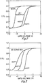
- Figure 2 shows that the as-deposited film exhibits an unpinned C-V curve.
- the effective positive charge at the interface is approximately 1x1012 cm ⁇ 2 before annnealing.
- B-type CaF2 films were epitaxially deposited onto (111)Si substrates according to the process flow of Figure 1.
- a (111)Si substrate is cleaned in step 10 prior to CaF2 deposition by annealing the substrate in an MBE chamber at 950°C for 10 minutes, plus another 10 minutes with a Si flux equivalent to a deposition rate of 0.01 monolayer/sec, for example.
- reflection high-energy electron diffraction (RHEED) and Auger spectroscopy for example, are used to characterize the cleaning process.
- step 14 CaF2 is deposited onto the (111)Si substrate surface by molecular beam epitaxy (MBE) from an effusion cell with a deposition rate of 4nm/min and to a film thickness of 100nm.
- MBE molecular beam epitaxy
- the temperature of the substrate is controlled and maintained at a predetermined fixed temperature of 800°C.
- the film was annealed, as shown in step 18, in forming gas (10% H2 in N2) at 450°C, 600°C, and 800°C for 30 minutes, and then patterned with Al dots for capacitance measurements.
- Figure 3 shows that the as-deposited film exhibits a pinned C-V curve, suggesting an unacceptable amount of interface states.
- the positive interface charge is reduced to 1.7x1011 cm ⁇ 2, 6.9x1011 cm ⁇ 2, and 1.2x1012 cm ⁇ 2 for annealing temperatures of 450°C, 600°C, and 800°C, respectively.
- Improved C-V characteristics are also observed when CaF2 films are annealed in F2 gas.
- the capacitors are not as stable as those annealed in hydrogen.
- the pinning and unpinning of these capacitor's may be caused by the dissociation of interfacial Ca-F-Si bonds during high temperature growth and the formation of a hydrogen or fluorine terminated Si interface after annealing in the H2 or F2. It is generally agreed that, for CaF2 grown at high temperatures, the CaF2/Si interface is predominantly Ca-Si bonds (see R.M. Tromp and M.C. Reuter, Physical Review Letters, 61, 1756 (1988), and J.L. Batstone and J.M. Phillips, Physical Review Letters, 61, 2275 (1988), and J. Zegenhagen and J.R. Patel, Physical Review B, 41, 5315 (1990)).
- inventive process of annealing the substrate on which the CaF2 is deposited can also be done during and/or after the process of forming semiconductor devices on the substrate.
Applications Claiming Priority (2)
| Application Number | Priority Date | Filing Date | Title |
|---|---|---|---|
| US07/843,038 US5229333A (en) | 1992-02-28 | 1992-02-28 | Method for improving the interface characteristics of CaF2 on silicon |
| US843038 | 1992-02-28 |
Publications (3)
| Publication Number | Publication Date |
|---|---|
| EP0562273A2 true EP0562273A2 (de) | 1993-09-29 |
| EP0562273A3 EP0562273A3 (en) | 1993-11-10 |
| EP0562273B1 EP0562273B1 (de) | 2001-01-31 |
Family
ID=25288913
Family Applications (1)
| Application Number | Title | Priority Date | Filing Date |
|---|---|---|---|
| EP93102540A Expired - Lifetime EP0562273B1 (de) | 1992-02-28 | 1993-02-18 | Verfahren zur Verbesserung der Eigenschaften der Grenzfläche CaF2 auf Silizium |
Country Status (4)
| Country | Link |
|---|---|
| US (1) | US5229333A (de) |
| EP (1) | EP0562273B1 (de) |
| JP (1) | JPH06256949A (de) |
| DE (1) | DE69329897T2 (de) |
Families Citing this family (8)
| Publication number | Priority date | Publication date | Assignee | Title |
|---|---|---|---|---|
| US5529640A (en) * | 1993-06-21 | 1996-06-25 | Texas Instruments Incorporated | Epitaxial metal-insulator-metal-semiconductor structures |
| US5494850A (en) * | 1994-03-01 | 1996-02-27 | Texas Instruments Incorporated | Annealing process to improve optical properties of thin film light emitter |
| JPH08213640A (ja) | 1994-08-15 | 1996-08-20 | Texas Instr Inc <Ti> | 窒化iii−v化合物共鳴トンネリングダイオード |
| JPH08107068A (ja) * | 1994-10-03 | 1996-04-23 | Nec Corp | MBE法によるSi基板上CdTe成長方法 |
| US5563428A (en) * | 1995-01-30 | 1996-10-08 | Ek; Bruce A. | Layered structure of a substrate, a dielectric layer and a single crystal layer |
| US6083849A (en) * | 1995-11-13 | 2000-07-04 | Micron Technology, Inc. | Methods of forming hemispherical grain polysilicon |
| US6534348B1 (en) | 1998-04-14 | 2003-03-18 | Texas Instruments Incorporated | Ultrascaled MIS transistors fabricated using silicon-on-lattice-matched insulator approach |
| US20020142478A1 (en) * | 2001-03-28 | 2002-10-03 | Hiroyuki Wado | Gas sensor and method of fabricating a gas sensor |
-
1992
- 1992-02-28 US US07/843,038 patent/US5229333A/en not_active Expired - Lifetime
-
1993
- 1993-02-18 DE DE69329897T patent/DE69329897T2/de not_active Expired - Fee Related
- 1993-02-18 EP EP93102540A patent/EP0562273B1/de not_active Expired - Lifetime
- 1993-02-26 JP JP5038570A patent/JPH06256949A/ja active Pending
Non-Patent Citations (6)
| Title |
|---|
| APPLIED PHYSICS LETTERS. vol. 56, no. 16, 16 April 1990, NEW YORK US pages 1567 - 1569 SINGH ET AL 'Planar stress relaxation in solid phase epitaxial CaF2 films grown on (111)Si by in situ rapid isothermal processing' * |
| APPLIED PHYSICS LETTERS. vol. 57, no. 11, 10 November 1990, NEW YORK US pages 1108 - 1110 TIWARI ET AL 'Molecular beam epitaxial growth of (100) oriented CdTe on Si(100) using BaF2-CaF2 as a buffer' * |
| APPLIED PHYSICS LETTERS. vol. 60, no. 3, 20 January 1992, NEW YORK US pages 338 - 340 CHO ET AL 'Electrical properties of low-temperature-grown CaF2 on Si(111)' * |
| JOURNAL OF APPLIED PHYSICS. vol. 67, no. 8, 15 April 1990, NEW YORK US pages 3744 - 3749 PAUL ET AL 'Fluoride dielectric films on Inp for metal-insulator-semiconductor applications' * |
| JOURNAL OF THE ELECTROCHEMICAL SOCIETY vol. 133, no. 1, January 1986, MANCHESTER, NEW HAMPSHIRE US pages 224 - 227 PHILLIPS ET AL 'Post-growth annealing treatments of epitaxial CaF2 on Si(100)' * |
| JOURNAL OF VACUUM SCIENCE AND TECHNOLOGY: PART B. vol. 6, no. 2, April 1988, NEW YORK US page 720 TU ET AL 'Molecular beam epitaxial growth of lattice-matched GaAs/(Ca,Sr)F2/Ge(100) heterostructures' * |
Also Published As
| Publication number | Publication date |
|---|---|
| DE69329897T2 (de) | 2001-07-19 |
| DE69329897D1 (de) | 2001-03-08 |
| EP0562273B1 (de) | 2001-01-31 |
| US5229333A (en) | 1993-07-20 |
| JPH06256949A (ja) | 1994-09-13 |
| EP0562273A3 (en) | 1993-11-10 |
Similar Documents
| Publication | Publication Date | Title |
|---|---|---|
| US6562703B1 (en) | Molecular hydrogen implantation method for forming a relaxed silicon germanium layer with high germanium content | |
| US4975387A (en) | Formation of epitaxial si-ge heterostructures by solid phase epitaxy | |
| US6404027B1 (en) | High dielectric constant gate oxides for silicon-based devices | |
| US11699615B2 (en) | High resistivity semiconductor-on-insulator wafer and a method of manufacture | |
| US6469357B1 (en) | Article comprising an oxide layer on a GaAs or GaN-based semiconductor body | |
| CA1283490C (en) | Method for passivating a compound semiconductor surface and device having improved semiconductor- insulator interface | |
| JP2666757B2 (ja) | Soi基板の製造方法 | |
| US5605860A (en) | Method of fabricating semiconductor thin film and method of fabrication Hall-effect device | |
| US4448633A (en) | Passivation of III-V semiconductor surfaces by plasma nitridation | |
| US20030193061A1 (en) | Electronic component and method for producing an electronic component | |
| US7348226B2 (en) | Method of forming lattice-matched structure on silicon and structure formed thereby | |
| Cho et al. | Epitaxial relations and electrical properties of low‐temperature‐grown CaF2 on Si (111) | |
| US5229333A (en) | Method for improving the interface characteristics of CaF2 on silicon | |
| Miura et al. | The effect of hot electron injection on interface charge density at the silicon to silicon dioxide interface | |
| US5364468A (en) | Method for the growth of epitaxial metal-insulator-metal-semiconductor structures | |
| US5753040A (en) | Method for the growth of epitaxial metal-insulator-metal-semiconductor structures | |
| US4000020A (en) | Vapor epitaxial method for depositing gallium arsenide phosphide on germanium and silicon substrate wafers | |
| Yu et al. | Properties of epitaxial SrTiO3 thin films grown on silicon by molecular beam epitaxy | |
| US7169619B2 (en) | Method for fabricating semiconductor structures on vicinal substrates using a low temperature, low pressure, alkaline earth metal-rich process | |
| EP0543759A2 (de) | Polykristalline Emitterkontaktanordnung mit einer verbesserten Kontrol-Zwischenschicht | |
| Chau et al. | The effects of deposition temperature on properties of SiO2 films fabricated by a new electron cyclotron resonance microwave plasma-enhanced chemical-vapor deposition process | |
| KR950002178B1 (ko) | 실리콘기판상에 성장된 GaAs에피택셜층의 유기금속화학증착법에 의한 델타-도핑형성방법 | |
| Sarrabayrouse et al. | Feasibility and electrical properties of 600° C thermal silica layers for thin film transistor applications | |
| Oleszek et al. | Heteroepitaxial Growth of SixGe1− x Alloys by Thermal Decomposition of SiH4 and GeH4 | |
| US5175129A (en) | Method of fabricating a semiconductor structure having an improved polysilicon layer |
Legal Events
| Date | Code | Title | Description |
|---|---|---|---|
| PUAI | Public reference made under article 153(3) epc to a published international application that has entered the european phase |
Free format text: ORIGINAL CODE: 0009012 |
|
| PUAL | Search report despatched |
Free format text: ORIGINAL CODE: 0009013 |
|
| AK | Designated contracting states |
Kind code of ref document: A2 Designated state(s): DE FR GB IT NL |
|
| AK | Designated contracting states |
Kind code of ref document: A3 Designated state(s): DE FR GB IT NL |
|
| 17P | Request for examination filed |
Effective date: 19940427 |
|
| 17Q | First examination report despatched |
Effective date: 19940609 |
|
| GRAG | Despatch of communication of intention to grant |
Free format text: ORIGINAL CODE: EPIDOS AGRA |
|
| 17Q | First examination report despatched |
Effective date: 19940609 |
|
| GRAG | Despatch of communication of intention to grant |
Free format text: ORIGINAL CODE: EPIDOS AGRA |
|
| GRAH | Despatch of communication of intention to grant a patent |
Free format text: ORIGINAL CODE: EPIDOS IGRA |
|
| GRAH | Despatch of communication of intention to grant a patent |
Free format text: ORIGINAL CODE: EPIDOS IGRA |
|
| GRAA | (expected) grant |
Free format text: ORIGINAL CODE: 0009210 |
|
| ITF | It: translation for a ep patent filed | ||
| AK | Designated contracting states |
Kind code of ref document: B1 Designated state(s): DE FR GB IT NL |
|
| PG25 | Lapsed in a contracting state [announced via postgrant information from national office to epo] |
Ref country code: FR Free format text: THE PATENT HAS BEEN ANNULLED BY A DECISION OF A NATIONAL AUTHORITY Effective date: 20010131 |
|
| REF | Corresponds to: |
Ref document number: 69329897 Country of ref document: DE Date of ref document: 20010308 |
|
| ET | Fr: translation filed | ||
| PG25 | Lapsed in a contracting state [announced via postgrant information from national office to epo] |
Ref country code: NL Free format text: LAPSE BECAUSE OF NON-PAYMENT OF DUE FEES Effective date: 20010901 |
|
| NLV4 | Nl: lapsed or anulled due to non-payment of the annual fee |
Effective date: 20010901 |
|
| PLBE | No opposition filed within time limit |
Free format text: ORIGINAL CODE: 0009261 |
|
| STAA | Information on the status of an ep patent application or granted ep patent |
Free format text: STATUS: NO OPPOSITION FILED WITHIN TIME LIMIT |
|
| REG | Reference to a national code |
Ref country code: GB Ref legal event code: IF02 |
|
| 26N | No opposition filed | ||
| REG | Reference to a national code |
Ref country code: FR Ref legal event code: ST |
|
| PGFP | Annual fee paid to national office [announced via postgrant information from national office to epo] |
Ref country code: IT Payment date: 20070628 Year of fee payment: 15 |
|
| PGFP | Annual fee paid to national office [announced via postgrant information from national office to epo] |
Ref country code: DE Payment date: 20080229 Year of fee payment: 16 Ref country code: GB Payment date: 20080108 Year of fee payment: 16 |
|
| PG25 | Lapsed in a contracting state [announced via postgrant information from national office to epo] |
Ref country code: IT Free format text: LAPSE BECAUSE OF NON-PAYMENT OF DUE FEES Effective date: 20080218 |
|
| GBPC | Gb: european patent ceased through non-payment of renewal fee |
Effective date: 20090218 |
|
| PG25 | Lapsed in a contracting state [announced via postgrant information from national office to epo] |
Ref country code: DE Free format text: LAPSE BECAUSE OF NON-PAYMENT OF DUE FEES Effective date: 20090901 |
|
| PG25 | Lapsed in a contracting state [announced via postgrant information from national office to epo] |
Ref country code: GB Free format text: LAPSE BECAUSE OF NON-PAYMENT OF DUE FEES Effective date: 20090218 |