EP0562614A2 - Verfahren und Vorrichtung zur Kontrolle eines lötfreien Verbinders durch Bildbearbeitung - Google Patents
Verfahren und Vorrichtung zur Kontrolle eines lötfreien Verbinders durch Bildbearbeitung Download PDFInfo
- Publication number
- EP0562614A2 EP0562614A2 EP93104980A EP93104980A EP0562614A2 EP 0562614 A2 EP0562614 A2 EP 0562614A2 EP 93104980 A EP93104980 A EP 93104980A EP 93104980 A EP93104980 A EP 93104980A EP 0562614 A2 EP0562614 A2 EP 0562614A2
- Authority
- EP
- European Patent Office
- Prior art keywords
- solderless terminal
- inspecting
- solderless
- image
- terminal
- Prior art date
- Legal status (The legal status is an assumption and is not a legal conclusion. Google has not performed a legal analysis and makes no representation as to the accuracy of the status listed.)
- Granted
Links
Images




Classifications
-
- G—PHYSICS
- G01—MEASURING; TESTING
- G01R—MEASURING ELECTRIC VARIABLES; MEASURING MAGNETIC VARIABLES
- G01R31/00—Arrangements for testing electric properties; Arrangements for locating electric faults; Arrangements for electrical testing characterised by what is being tested not provided for elsewhere
- G01R31/28—Testing of electronic circuits, e.g. by signal tracer
- G01R31/302—Contactless testing
- G01R31/308—Contactless testing using non-ionising electromagnetic radiation, e.g. optical radiation
-
- G—PHYSICS
- G01—MEASURING; TESTING
- G01N—INVESTIGATING OR ANALYSING MATERIALS BY DETERMINING THEIR CHEMICAL OR PHYSICAL PROPERTIES
- G01N21/00—Investigating or analysing materials by the use of optical means, i.e. using sub-millimetre waves, infrared, visible or ultraviolet light
- G01N21/84—Systems specially adapted for particular applications
- G01N21/88—Investigating the presence of flaws or contamination
- G01N21/8806—Specially adapted optical and illumination features
-
- H—ELECTRICITY
- H01—ELECTRIC ELEMENTS
- H01R—ELECTRICALLY-CONDUCTIVE CONNECTIONS; STRUCTURAL ASSOCIATIONS OF A PLURALITY OF MUTUALLY-INSULATED ELECTRICAL CONNECTING ELEMENTS; COUPLING DEVICES; CURRENT COLLECTORS
- H01R43/00—Apparatus or processes specially adapted for manufacturing, assembling, maintaining, or repairing of line connectors or current collectors or for joining electric conductors
- H01R43/04—Apparatus or processes specially adapted for manufacturing, assembling, maintaining, or repairing of line connectors or current collectors or for joining electric conductors for forming connections by deformation, e.g. crimping tool
- H01R43/048—Crimping apparatus or processes
Definitions
- the present invention relates to a method and apparatus for inspecting a solderless terminal which has been crimped against one end portion of an electric conductor. More specifically, the invention relates to a method and apparatus for illuminating and image processing to inspect a solderless terminal to determine whether or not the solderless terminal has been satisfactorily crimped against an electric conductor.
- Figure 21 shows a solderless terminal 2 comprising a cylindrical shaped resin barrel 2a holding a resin cover 1a near one end portion of an electric conductor 1 which has the resin cover 1a removed, a core wire barrel 2b which also has a cylindrical shape to hold the one end portion of the electric conductor 1 having the resin cover 1a removed, a plurality of core wires 1b comprising the electric conductor 1, and an end portion 2c which is engaged with a mating solderless terminal so as to be electrically connected to the solderless terminal.
- bell mouths 10 are formed at both ends of the core wire barrel 2b to release stress produced by crimping the solderless terminal 2 against the electric conductor 1.
- an inspecting apparatus as shown in Figure 22 has been used in inspecting the solderless terminal 2 by image processing.
- the solderless terminal To inspect how a solderless terminal and electric conductor are crimped, the solderless terminal must first be illuminated as described later.
- the image of a solderless terminal 2 produced by illumination is picked up by image pick-up means 3 such as a television camera or a two-dimensional CCD camera, and displayed on a monitoring television set or monitor.
- image pick-up means 3 such as a television camera or a two-dimensional CCD camera
- the image is processed by image processing means 5, so that the resulting luminance data of the picture elements of the image are utilized to determine the presence or absence of the resin cover 1a and the core wires 1b between the resin barrel 2a and the core wire barrel 2b.
- the resulting luminance data is also used to determine the exposure of the core wires 1b located between the core wire barrel 2b and the end portion 2c to judge whether or not the solderless terminal 2 has been satisfactorily crimped against an electric conductor.
- the results of these determinations are printed out by a printer 6, or displayed on a display unit 7.
- reference numeral 8 designates an operation keyboard, with which program data or the like are inputted for an image processing operation.
- Japanese Patent Application (OPI) No. 175942 discloses a method in which contrast between a resin portion and a metal portion is obtained by using polarized light. Furthermore, Japanese Patent Application (OPI) No. 198473 discloses a method in which contrast between a resin portion and a metal portion is obtained by using a light beam of a particular wavelength which the resin material readily absorbs.
- the above-described conventional illuminating methods have several drawbacks. Whenever a resin color is changed, it is necessary to select either a complementary color filter suitable for the new resin color, or a light beam having a wavelength suitable for the new resin color. That is, different complementary color filters or different light beams must be used for different resin colors thereby increasing the cost and required maintenance. In addition, it is impossible for either of the illuminating methods to accurately obtain the necessary contrast between a resin portion and metal portion. Thus, the conventional methods cannot accurately determine if a solderless terminal has been satisfactorily crimped against the electric conductor.
- An object of the present invention is to eliminate the above-described difficulties associated with the conventional illuminating methods for inspecting a crimped solderless terminal.
- Another object of the present invention is to provide a more accurate method and apparatus for determining whether a solderless terminal has been satisfactorily crimped against
- Another object of the present invention is to improve the accuracy of a processed image of a solderless terminal by producing and accurately detecting a greater contrast between a resin portion and a metal portion of a solderless terminal.
- the solderless terminal comprises a resin barrel adapted to hold an end portion of an electric conductor which has its resin cover removed therefrom to expose core wires at the end.
- the solderless terminal further comprises a core barrel adapted to hold the exposed core wires of the electric conductor so that the electric conductor is electrically connected to the solderless terminal.
- the illuminating method and apparatus of the present invention includes main illuminating means having at least one illuminating element extending substantially in the same direction as the length of the solderless terminal.
- the main illuminating means comprises a plurality of illuminating elements arranged substantially in the same direction as the length of the solderless terminal.
- the main illuminating means illuminates the solderless terminal in substantially the same direction as an image pick-up direction of the image pick-up means.
- the illuminating apparatus also includes auxiliary illuminating means for illuminating the solderless terminal in a direction which is opposite to the direction in which the main illuminating means illuminates the solderless terminal.
- the solderless terminal After the solderless terminal is illuminated by the illuminating apparatus and an image of the solderless terminal is picked up by image pick-up means in a direction substantially perpendicular to the cylindrical surfaces of the barrels, the image picked up by image pick-up means is processed by image processing means to inspect how the solderless terminal has been crimped against the electric conductor.
- an image processing method and apparatus for inspecting a solderless terminal by image processing as described above wherein an area histogram of optical intensity of the image of the solderless terminal is obtained in advance by means of the image processing means.
- an area histogram of optical intensity of the image of the solderless terminal is obtained in advance by means of the image processing means.
- binary levels are provided for a region between a specular reflection region of each of the barrels and a background region, and a region between the background region and non-specular reflection thereof.
- the image of the solderless terminal picked up by the image pick-up means is binary-coded by using the binary levels.
- the main illuminating means having an illuminating element extending substantially in the same direction as a length of the solderless terminal illuminates the solderless terminal in substantially the same direction as the image pick-up direction of the image pick-up means.
- the auxiliary illuminating means illuminates the solderless terminal in a direction opposite to the illumination direction of the main illuminating means.
- the main illuminating means and the auxiliary illuminating means illuminate the solderless terminal, and, in the area histogram obtained, the image of the solderless terminal is binary-coded by using one binary level set for the region between the specular reflection region and the background region, and another binary level set for the region between the background region and the non-specular reflection region. Therefore, in the case where any one of the core wires of the conductor extends outside of the solderless terminal, these wires can be accurately detected irrespective of the direction of extension of the core wires and thereby detect that the solderless terminal has been unsatisfactorily crimped against the electric conductor.
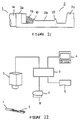
- Figure 1 is a side elevation view of a first embodiment of the solderless terminal inspecting apparatus of the present invention.
- Figure 2 is a front elevation view of the first embodiment shown in Figure 1.
- Figure 3 is a schematic view of an image picked up by the image pick-up means of the first embodiment including specular reflection portions.
- Figure 4 is a schematic view of only the specular reflection portions of Figure 3.
- Figure 5 is a schematic view of intersections of windows W1, W2 used to detect reference point A.
- Figure 6 is a schematic view of the detected reference point A.
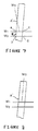
- Figure 7 is a schematic view of the detected reference point A having an inclination error angle of ⁇ .
- Figure 8 is a schematic view of a shifted position of windows W1, W2 to compensate for the inclination error angle of ⁇ .
- Figure 9A is a graph of an area histogram of optical intensity corresponding to barrels 2a and 2b.
- Figure 9B is a graph of an area histogram of only the background without the solderless terminal.
- Figure 9C is a graph of an area histogram resulting from combination of graphs of Figures 9A and 9B.
- Figure 10A is a graph of an area histogram when a white electric conductor is used.
- Figure 10B is a graph of an area histogram when a black electric conductor is used.
- Figure 11A is a front view elevation depicting the state where a core wire is pushed out of the core wire barrel 2b.
- Figure 12 is an elevation view along line X-X' of Figure 11A.
- Figure 13 is a side elevation view showing a core wire pushed out of a resin barrel.
- Figure 14 is a schematic view of windows Wa, Wb, Wc and Wd.
- Figure 15 is a graph of an area histogram of optical intensity of windows Wa, Wb, Wc and Wd.
- Figure 16A is a top perspective view of a satisfactorily crimped solderless terminal.
- Figure 16B is a side perspective view of Figure 16A.
- Figure 17A is a top perspective view of an unsatisfactorily crimped solderless terminal.
- Figure 17B is a side perspective view of Figure 17A.
- Figure 18A is a top perspective view of an unsatisfactorily crimped solderless terminal.
- Figure 18B is a side perspective view of Figure 18A.
- Figure 19 is a side elevation view of a second embodiment of the solderless terminal inspecting apparatus of the present invention.
- Figure 20A is a side elevation view of a third embodiment of the solderless terminal inspecting apparatus of the present invention.
- Figure 20B is front elevation view of a third embodiment of the solderless terminal inspecting apparatus of the present invention.
- FIG. 21 is a side elevation view of a solderless terminal.
- FIG. 22 is schematic view of an image processing means relating to the present invention used for inspecting solderless terminals.
- solderless terminal to be inspected by the method and apparatus of the present invention is assumed to have a fundamental structure substantially similar to the one shown in Figure 21.
- the image processing means employed in the present invention is the similar to the one shown in FIG. 22. Therefore, in the following description of the invention, reference numerals used in Figures 21 and 22 are used to refer to identical elements in Figures 1-20.
- the first embodiment of the invention comprises a main illuminating means 11 having a pair of illuminating elements 11a, 11b disposed parallel to each other.
- Illuminating elements 11a, 11b may comprise bar-shaped fluorescent lamps which extend longitudinally along the length of solderless terminal 2.
- Illuminating elements 11a, 11b are driven by a high frequency power source 12 of the order of about 20 kHz to illuminate solderless terminal 2.
- An auxiliary illuminating means 13 is provided on the other side of solderless terminal 2 to illuminate solderless terminal 2 in a direction opposite to the illumination of main illumination means 11.
- the arrows indicate that some of the light beams are scattered, for instance, by the paint layer on the surface of main illuminating means 11 and applied to solderless terminal 2.
- illuminating elements 11a, 11b are so arranged that they illuminate solderless terminal 2 in a direction which is substantially the same as the image pick-up direction of image pick-up means 3. That is, illuminating elements 11a, 11b illuminate solderless terminal 2 in a direction which is substantially perpendicular to the cylindrically shaped surfaces of barrels 2a and 2b.
- a light shielding board 14 is provided over main illuminating means 11 so that light from illuminating elements 11a, 11b is not applied directly to image pick-up means 3.
- Light beams emitted from illuminating elements 11a, 11b are specularly reflected by the cylindrically shaped surfaces of resin barrel 2a and core wire barrel 2b of solderless terminal 2.
- the light beams reflected off of resin barrel 2a and core wire barrel 2b then travel to image pick-up means 3.
- the illuminating light beams from illuminating elements 11a, 11b which are not reflected by solderless terminal 2 are reflected by auxiliary illuminating means 13, thus illuminating solderless terminal 2 in a direction opposite to the illumination direction of illuminating elements 11a, 11b. That is, illuminating elements 11a, 11b illuminate from a top side of solderless terminal 2 and auxiliary illuminating means 13 illuminates from a bottom side of solderless terminal 2.
- FIG 3 The image of solderless terminal 2 thus illuminated is shown in Figure 3.
- the cross-hatched portions in Figure 3 illustrate a distribution of specular reflections comprised of specular reflection portions.
- specular reflection takes place between the resin barrel 2a and the core wire barrel 2b. That is, the light beams are specularly reflected by core wires 1b exposed between barrels 2a and 2b.
- Figure 4 shows those specular reflection portions only.
- bell mouths 10 are provided at both ends of core wire barrel 2b. Bell mouths 10 distinguish the borders between the specular reflection portions of core wire barrel 2b and exposed core wires 1b.
- the image processing reference points are determined according to a run length coding method, disclosed in detail in Japanese Patent Application No. 268771 filed by the present Applicant, the disclosure of which is hereby incorporated by reference. That is, the configuration of a solderless terminal being inspected is detected from variations in white and black data along scanning lines.
- windows W1 and W2 in the form of straight lines as shown in Figure 5 are provided in such a manner that they are laid across the central portion of the image of one of the specular reflection portions of core wire barrel 2b. That is, intersections a, b, c and d of the windows W1 and W2 and the border lines of the specular reflection portions are obtained.
- the gradient of the specular reflection portion can be obtained from the gradient of the segment a-b.
- a window W3 is drawn in such a manner that the window W3 extends from the midpoint of the segment a-b, or from any point on the segment a-b, and has the same gradient as the segment a-b. Under this condition, the point A on the window W where luminance is changed is detected. This point A is one of the reference points necessary for image processing.
- other reference points B, C, D, E, F, G and H are determined as shown in Figure 4.
- barrels 2a and 2b are not completely cylindrical, and thus, less than completely specular reflections result. Therefore, the specular reflection portions are geometrically inaccurate and unstable. Hence, it is difficult to determine the reference points by performing the above-described processing operation only once as shown in Figures 5 and 6. That is, in order to obtain accurate reference points, the processing operation must be performed two or three times.
- the location of the terminal 2 in Figure 7 includes an error shown by the inclination angle ⁇ of the segment a-b. Therefore, if the window W3 is set as shown in Figure 7, the reference point A' is not located at the end of the specular reflection portion. Accordingly, as shown in Figure 8, the windows W1 and W2 are set in a position which is shifted as much as several picture elements from the reference point A'. Then, the same processing operation is carried out again to determine the point on the window W3 where luminance is changed, referred to as a luminance change point.
- the configuration, dimension and inclination of the solderless terminal can be obtained with reference to those reference points A through H. And whether or not the state of solderless terminal 2 is acceptable is determined from the position of the end of resin cover 1a between resin barrel 1a and core wire barrel 2b. Also determined is the amount of protrusion of the core wires 1b between core wire barrel 2b and end portion 2c.
- solderless terminal 2 Since the reference points A through H are determined with high accuracy, it is unnecessary to hold solderless terminal 2 in one particular position with mechanical means such as a chuck. That is, it is not always necessary to accurately position the solderless terminal 1 being inspected. It is assumed that for inspection of a solderless terminal 2, solderless terminal 2 is set parallel to the X-Y plane with the width of solderless terminal perpendicular to the longitudinal direction of solderless terminal 2 set parallel to the Y-axis. It is also assumed that main illuminating means 11 and light elements 11a, 11b are arranged in the same orientation, and the image of the solderless terminal is picked up in the direction of Z-axis.
- solderless terminal 2 may be shifted either towards the X-axis or the Y-axis as long as it is in the visual field of image pick-up means 3.
- the-focus of image pick-up means 3 should be adjusted. It has been confirmed through experiment that, in the case of a so-called "yawing" where solderless terminal 2 turns about the Z-axis, the image can be accurately obtained even if solderless terminal 2 is displaced about ⁇ 45° from its fundamental position.
- FIG. 9A An area histogram of optical intensity of the image of solderless terminal 2 crimped against a blue electric conductor 1 is shown in Figure 9A.
- the horizonal axis represents luminance levels indicated in 256 gradations, while the vertical axis represents areas (the numbers of picture elements).
- the region P which displays a high luminance level corresponds to the specular reflection portions of barrels 2a and 2b.
- the region Q displaying a middle luminance level corresponds to the resin portion of the electric conductor 1.
- the region R displays a low luminance level which corresponds to a non-specular reflection portion of solderless terminal 2.
- FIG. 9B An area histogram of optical intensity-of the image of only the background without the solderless terminal is shown in Figure 9B. That is, a background region Q' corresponding to the above-described resin region Q displays a peak. In this case, an irregular reflection board is selected as the auxiliary illuminating means 13 so that the background region Q' is between the specular reflection region P and the non-specular reflection region R.
- the area histograms shown in Figures 9A and 9B may be combined into the histogram shown in Figure 9C.
- the specular reflection region P, the background region Q'', and the non-specular reflection region R of Figure 9C have peaks and valleys between the regions P and Q'', and between the regions Q'' and R.
- an area histogram of a typical solderless terminal 2 is obtained in advance, and binary levels are set for the valley between the specular reflection region P and the background region Q'', and the valley between the background region Q'' and the non-specular reflection region R, respectively.
- a binary level can be set for the valley between the specular reflection region P and the resin region Q, and a binary level can be set for the valley between the resin region Q and the non-specular reflection region R by controlling the intensity of illumination.
- the intensity of illumination can be controlled by adjusting the aperture of the lens of image pick-up means 3.
- two different binary levels can be set for those valleys, and stored in the image processing means 5 shown in Figure 22.
- One binary level can be set for this wide valley.
- the white electric conductor 1 by obtaining an area histogram of a typical solderless terminal in advance, as in the case of the blue electric conductor, two binary levels can be set according to the area histogram obtained in advance.
- the black electric conductor only one binary level can be set according to the area histogram.
- another binary level can be readily set for a low luminance region according to other area histograms.
- solderless terminal 2 illuminated by the main illuminating means 11 and auxiliary illuminating means 13 in opposite directions, two different binary levels are set according to the area histogram of optical intensity of the image of the illuminated solderless terminal. Then core wires located outside or on the side of the solderless terminal can be detected accurately.
- the core wire L may or may not give rise to specular reflection. This depends on whether the core wire L is extended in the direction of the X-axis, or extended in the direction of the Y-axis, or extended in the direction of the Z-axis. Sometimes good contrast cannot be obtained because of the location of the core wire L. Thus, detection of the core wire located outside of solderless terminal 2 cannot be accomplished by processing the image with only one binary level. Therefore, the image of solderless terminal 2 is obtained by illuminating solderless terminal 2 from both sides with main illuminating means 11 and auxiliary illuminating means 13.
- the core wire L can be detected by assigning a binary code according to the binary levels which have been set for the valley between the regions P and Q' and the valley between the regions Q' and R, to the luminance of the picture elements of the windows Wa through Wd. Thereafter, it is determined whether or not there is a picture element having a luminance value higher than the higher binary level set for the valley between the regions P and Q', and whether or not there is a picture element having a luminance value lower than the lower binary level set for the valley between the regions Q' and R. As a result of this determination, the core wire L extending outside of solderless terminal 2 can be detected irrespective of the direction in which the core wire extends.
- solderless terminal 2 has been satisfactorily crimped against electric conductor 1.
- the reference points necessary for the image processing operation can be detected with high accuracy.
- the core wire extended to the side of solderless terminal 1 can be detected accurately. That is, it can be determined with high reliability whether or not the solderless terminal has been satisfactorily crimped against the electric conductor.
- a second embodiment of the invention is shown in Figure 19.
- main illuminating means 11 instead of main illuminating means 11 being comprised of bar-shaped fluorescent lamps as shown in Figure 1, main illuminating means 15 is made up of arcuate fluorescent lamps or the like.
- the second embodiment produces the same resulting effects as the first embodiment. Also, since the curved front end portion of main illuminating means 15 of the second embodiment is closer to solderless terminal 2 than the base end portion thereof, the bundle of rays from the main illuminating means is increased in width thereby contributing to improvement of the image processing accuracy.
- main illuminating means 17 are made up of a plurality of illuminating elements 16 such as light emitting diodes arranged in a direction which is substantially the same as the direction in which the length of solderless terminal 2 is positioned.
- the third embodiment produces the same effects as the first embodiment, as well as resulting in miniaturization of main illuminating means 17 and reduction of the manufacturing cost of main illuminating means 17.
- the plurality of illuminating elements 16 may be arranged arcuately as in the case of the second embodiment shown in Figure 19.
- the auxiliary illuminating means comprises a white irregular reflection board.
- irregular reflection boards of other colors may be employed, or a light source may be provided in addition to main illuminating means 11, 15 and 17. That is, all that is required for the auxiliary illuminating means is that, in the area histogram, the background region Q' (FIG. 9B) is between the specular reflection region P and the non-specular refection region R ( Figures 9A and 9C).
- the technical concept of the invention is applicable to inspection of all types of solderless terminals which comprise a resin barrel and a core wire barrel, and can be applied to motor vehicle harnesses or other harnesses.
Landscapes
- Physics & Mathematics (AREA)
- General Physics & Mathematics (AREA)
- Health & Medical Sciences (AREA)
- Engineering & Computer Science (AREA)
- Analytical Chemistry (AREA)
- Biochemistry (AREA)
- General Engineering & Computer Science (AREA)
- Electromagnetism (AREA)
- Life Sciences & Earth Sciences (AREA)
- Chemical & Material Sciences (AREA)
- Computer Vision & Pattern Recognition (AREA)
- Toxicology (AREA)
- General Health & Medical Sciences (AREA)
- Immunology (AREA)
- Pathology (AREA)
- Length Measuring Devices By Optical Means (AREA)
- Image Analysis (AREA)
- Investigating Materials By The Use Of Optical Means Adapted For Particular Applications (AREA)
- Image Input (AREA)
- Image Processing (AREA)
Applications Claiming Priority (2)
| Application Number | Priority Date | Filing Date | Title |
|---|---|---|---|
| JP4102240A JP2795044B2 (ja) | 1992-03-26 | 1992-03-26 | 圧着端子画像処理検査における照明方法及び画像処理方法 |
| JP102240/92 | 1992-03-26 |
Publications (3)
| Publication Number | Publication Date |
|---|---|
| EP0562614A2 true EP0562614A2 (de) | 1993-09-29 |
| EP0562614A3 EP0562614A3 (en) | 1994-08-24 |
| EP0562614B1 EP0562614B1 (de) | 1998-06-03 |
Family
ID=14322112
Family Applications (1)
| Application Number | Title | Priority Date | Filing Date |
|---|---|---|---|
| EP93104980A Expired - Lifetime EP0562614B1 (de) | 1992-03-26 | 1993-03-25 | Verfahren und Vorrichtung zur Kontrolle eines lötfreien Verbinders durch Bildbearbeitung |
Country Status (4)
| Country | Link |
|---|---|
| US (1) | US5377278A (de) |
| EP (1) | EP0562614B1 (de) |
| JP (1) | JP2795044B2 (de) |
| DE (1) | DE69318872T2 (de) |
Cited By (4)
| Publication number | Priority date | Publication date | Assignee | Title |
|---|---|---|---|---|
| EP0649030A1 (de) * | 1993-10-18 | 1995-04-19 | Sumitomo Wiring Systems, Ltd. | Kontaktelementüberprüfungsmethode und Kontaktelementüberprüfungsvorrichtung |
| EP0702227A1 (de) * | 1994-09-14 | 1996-03-20 | Sumitomo Wiring Systems, Ltd. | Vorrichtung zur Untersuchung von Kabelenden in Maschinen zum Abisolieren und Anquetschen von Kabeln |
| EP0718594A3 (de) * | 1994-12-22 | 1998-03-11 | Sumitomo Wiring Systems, Ltd. | Verfahren und Vorrichtung zur Beleuchtung im Endstückinspektionsteil einer Drahtendstückproduktionsmaschine |
| US6738134B2 (en) | 2000-09-28 | 2004-05-18 | Yazaki Corporation | Inspection method and inspection system of a terminal metal fitting |
Families Citing this family (6)
| Publication number | Priority date | Publication date | Assignee | Title |
|---|---|---|---|---|
| JP3002388B2 (ja) * | 1994-09-14 | 2000-01-24 | 住友電装株式会社 | 皮剥端子圧着機における電線処理部検査装置 |
| KR0176661B1 (ko) * | 1995-12-28 | 1999-05-15 | 김광호 | 납땜부 검사방법 및 검사장치 |
| JP2006275836A (ja) * | 2005-03-30 | 2006-10-12 | Dainippon Screen Mfg Co Ltd | 基板検査装置 |
| JP4506718B2 (ja) * | 2006-04-28 | 2010-07-21 | 株式会社明電舎 | 圧着端子検査方法 |
| DE102008006457A1 (de) | 2008-01-29 | 2009-07-30 | Kromberg & Schubert Gmbh & Co. Kg | Verfahren und Vorrichtung für die Kontaktierung eines elektrischen Leiters |
| JP6911442B2 (ja) * | 2017-03-27 | 2021-07-28 | 住友電装株式会社 | 検査装置、および、検査方法 |
Family Cites Families (27)
| Publication number | Priority date | Publication date | Assignee | Title |
|---|---|---|---|---|
| JPS55142254A (en) * | 1979-04-25 | 1980-11-06 | Hitachi Ltd | Inspecting method for pattern of printed wiring board |
| JPS6017044B2 (ja) * | 1979-07-23 | 1985-04-30 | 株式会社日立製作所 | 印刷配線板のパタ−ン検査装置 |
| JPS5760249A (en) * | 1980-09-29 | 1982-04-12 | Shin Meiwa Ind Co Ltd | Terminal compression status inspecter for terminal compressed wire |
| JPS57175942A (en) * | 1981-04-23 | 1982-10-29 | Shin Meiwa Ind Co Ltd | Terminal pressing inspection device for solderless terminal wire |
| US4563095A (en) * | 1982-12-20 | 1986-01-07 | Essex Group, Inc. | Method and apparatus for monitoring the surface of elongated objects |
| US4573073A (en) * | 1983-06-02 | 1986-02-25 | General Electric Company | Integrated lighting and camera system |
| US4555799A (en) * | 1983-10-24 | 1985-11-26 | Sumitomo Electric Industries, Ltd. | Method for inspecting crimp bonded terminals |
| FR2553914B1 (fr) * | 1983-10-25 | 1986-01-03 | Sumitomo Electric Industries | Procede d'inspection de bornes connectees par sertissage |
| JPS60198473A (ja) * | 1984-03-21 | 1985-10-07 | Shin Meiwa Ind Co Ltd | 端子圧着電線の端子圧着状態検査装置 |
| JPS61133845A (ja) * | 1984-12-03 | 1986-06-21 | Shin Meiwa Ind Co Ltd | 圧着端子の把持部検査装置 |
| US4734766A (en) * | 1985-08-19 | 1988-03-29 | Kawasaki Steel Corporation | Method and system for locating and inspecting seam weld in metal seam-welded pipe |
| US4649621A (en) * | 1986-02-21 | 1987-03-17 | Artos Engineering Company | Wire processing apparatus having control means |
| US4922308A (en) * | 1986-06-27 | 1990-05-01 | Hitachi, Ltd. | Method of and apparatus for detecting foreign substance |
| US4760444A (en) * | 1987-07-22 | 1988-07-26 | Csd International, Inc. | Machine visual inspection device and method |
| US5072127A (en) * | 1987-10-09 | 1991-12-10 | Pressco, Inc. | Engineered video inspecting lighting array |
| US4975863A (en) * | 1988-06-16 | 1990-12-04 | Louisiana State University And Agricultural And Mechanical College | System and process for grain examination |
| FR2634551B1 (fr) * | 1988-07-20 | 1990-11-02 | Siderurgie Fse Inst Rech | Procede et dispositif d'identification du fini d'une surface metallique |
| US5073952A (en) * | 1988-09-07 | 1991-12-17 | Sigmax Kabushiki Kaisha | Pattern recognition device |
| US4975972A (en) * | 1988-10-18 | 1990-12-04 | At&T Bell Laboratories | Method and apparatus for surface inspection |
| JP2517381B2 (ja) * | 1989-01-18 | 1996-07-24 | 新明和工業株式会社 | 圧着端子の圧着状態検査装置 |
| US4988202A (en) * | 1989-06-28 | 1991-01-29 | Westinghouse Electric Corp. | Solder joint inspection system and method |
| US5060290A (en) * | 1989-09-05 | 1991-10-22 | Dole Dried Fruit And Nut Company | Algorithm for gray scale analysis especially of fruit or nuts |
| US5197105A (en) * | 1990-05-30 | 1993-03-23 | Dainippon Screen Mfg. Co. Ltd. | Method of reading optical image of inspected surface and image reading system employabale therein |
| JP2845601B2 (ja) * | 1990-10-09 | 1999-01-13 | 株式会社東芝 | ワイヤボンディング外観検査装置 |
| US5204911A (en) * | 1991-05-29 | 1993-04-20 | Nira Schwartz | Inspection method using unique templates and histogram analysis |
| US5235649A (en) * | 1991-06-13 | 1993-08-10 | Videk Corporation | Cigarette inspection method |
| US5187611A (en) * | 1991-08-27 | 1993-02-16 | Northeast Robotics, Inc. | Diffuse on-axis light source |
-
1992
- 1992-03-26 JP JP4102240A patent/JP2795044B2/ja not_active Expired - Lifetime
-
1993
- 1993-03-19 US US08/034,771 patent/US5377278A/en not_active Expired - Lifetime
- 1993-03-25 EP EP93104980A patent/EP0562614B1/de not_active Expired - Lifetime
- 1993-03-25 DE DE69318872T patent/DE69318872T2/de not_active Expired - Fee Related
Non-Patent Citations (1)
| Title |
|---|
| None |
Cited By (6)
| Publication number | Priority date | Publication date | Assignee | Title |
|---|---|---|---|---|
| EP0649030A1 (de) * | 1993-10-18 | 1995-04-19 | Sumitomo Wiring Systems, Ltd. | Kontaktelementüberprüfungsmethode und Kontaktelementüberprüfungsvorrichtung |
| US5583948A (en) * | 1993-10-18 | 1996-12-10 | Sumitomo Wiring Systems, Ltd. | Connecting element inspecting method and connecting element inspecting device |
| EP0702227A1 (de) * | 1994-09-14 | 1996-03-20 | Sumitomo Wiring Systems, Ltd. | Vorrichtung zur Untersuchung von Kabelenden in Maschinen zum Abisolieren und Anquetschen von Kabeln |
| US5691763A (en) * | 1994-09-14 | 1997-11-25 | Sumitomo Wiring Systems, Ltd. | Terminated cable portion inspection device for stripped terminal crimping machine |
| EP0718594A3 (de) * | 1994-12-22 | 1998-03-11 | Sumitomo Wiring Systems, Ltd. | Verfahren und Vorrichtung zur Beleuchtung im Endstückinspektionsteil einer Drahtendstückproduktionsmaschine |
| US6738134B2 (en) | 2000-09-28 | 2004-05-18 | Yazaki Corporation | Inspection method and inspection system of a terminal metal fitting |
Also Published As
| Publication number | Publication date |
|---|---|
| US5377278A (en) | 1994-12-27 |
| DE69318872D1 (de) | 1998-07-09 |
| EP0562614A3 (en) | 1994-08-24 |
| JPH05272939A (ja) | 1993-10-22 |
| DE69318872T2 (de) | 1999-02-11 |
| JP2795044B2 (ja) | 1998-09-10 |
| EP0562614B1 (de) | 1998-06-03 |
Similar Documents
| Publication | Publication Date | Title |
|---|---|---|
| US5293220A (en) | Method for inspecting stripped condition of electric wire | |
| US5208463A (en) | Method and apparatus for detecting deformations of leads of semiconductor device | |
| EP0702227B1 (de) | Vorrichtung zur Untersuchung von Kabelenden in Maschinen zum Abisolieren und Anquetschen von Kabeln | |
| US6738134B2 (en) | Inspection method and inspection system of a terminal metal fitting | |
| US5377278A (en) | Method and apparatus for inspecting a solderless terminal by image processing | |
| US5619792A (en) | Method and device for illumination in terminated cable part inspection device for stripped terminal crimping machine | |
| JP3935048B2 (ja) | 被覆電線検査装置 | |
| US6437355B1 (en) | Apparatus for judging whether bump height is proper or not | |
| JP3002389B2 (ja) | 皮剥端子圧着機における電線処理部検査装置 | |
| JPH02189880A (ja) | 圧着端子の圧着状態検査装置 | |
| JPH0621165A (ja) | 画像の二値化良否判別方法 | |
| JP7312663B2 (ja) | 線状物の作業位置決定方法、ロボットの制御方法、線状物の固定方法、線状物の作業位置決定装置および線状物把持システム | |
| JPH06213817A (ja) | 圧着端子画像処理検査における照明方法 | |
| JPH04329344A (ja) | 実装基板検査装置 | |
| JPS6353494B2 (de) | ||
| JPH05249043A (ja) | 圧着端子画像処理検査における照明方法 | |
| JP2818347B2 (ja) | 外観検査装置 | |
| JP2792362B2 (ja) | 圧着端子の圧着検査方法 | |
| JP3002388B2 (ja) | 皮剥端子圧着機における電線処理部検査装置 | |
| JP2962014B2 (ja) | 端子圧着位置検査装置 | |
| CN1168513A (zh) | 视觉识别装置及元件识别方法 | |
| JPS58135440A (ja) | 端子圧着電線の端子圧着状態検査装置 | |
| JPH07117391B2 (ja) | 照明ランプにおける端子のカシメ部の検査装置 | |
| JPS61213709A (ja) | 電子部品外観検査方法 | |
| JPH10170224A (ja) | はんだ付け外観検査方法及びその装置 |
Legal Events
| Date | Code | Title | Description |
|---|---|---|---|
| PUAI | Public reference made under article 153(3) epc to a published international application that has entered the european phase |
Free format text: ORIGINAL CODE: 0009012 |
|
| AK | Designated contracting states |
Kind code of ref document: A2 Designated state(s): DE GB |
|
| PUAL | Search report despatched |
Free format text: ORIGINAL CODE: 0009013 |
|
| AK | Designated contracting states |
Kind code of ref document: A3 Designated state(s): DE GB |
|
| 17P | Request for examination filed |
Effective date: 19941202 |
|
| 17Q | First examination report despatched |
Effective date: 19961223 |
|
| GRAG | Despatch of communication of intention to grant |
Free format text: ORIGINAL CODE: EPIDOS AGRA |
|
| GRAG | Despatch of communication of intention to grant |
Free format text: ORIGINAL CODE: EPIDOS AGRA |
|
| GRAH | Despatch of communication of intention to grant a patent |
Free format text: ORIGINAL CODE: EPIDOS IGRA |
|
| GRAH | Despatch of communication of intention to grant a patent |
Free format text: ORIGINAL CODE: EPIDOS IGRA |
|
| GRAA | (expected) grant |
Free format text: ORIGINAL CODE: 0009210 |
|
| AK | Designated contracting states |
Kind code of ref document: B1 Designated state(s): DE GB |
|
| REF | Corresponds to: |
Ref document number: 69318872 Country of ref document: DE Date of ref document: 19980709 |
|
| PLBE | No opposition filed within time limit |
Free format text: ORIGINAL CODE: 0009261 |
|
| 26N | No opposition filed | ||
| REG | Reference to a national code |
Ref country code: GB Ref legal event code: IF02 |
|
| PGFP | Annual fee paid to national office [announced via postgrant information from national office to epo] |
Ref country code: DE Payment date: 20050317 Year of fee payment: 13 |
|
| PGFP | Annual fee paid to national office [announced via postgrant information from national office to epo] |
Ref country code: GB Payment date: 20050323 Year of fee payment: 13 |
|
| PG25 | Lapsed in a contracting state [announced via postgrant information from national office to epo] |
Ref country code: GB Free format text: LAPSE BECAUSE OF NON-PAYMENT OF DUE FEES Effective date: 20060325 |
|
| PG25 | Lapsed in a contracting state [announced via postgrant information from national office to epo] |
Ref country code: DE Free format text: LAPSE BECAUSE OF NON-PAYMENT OF DUE FEES Effective date: 20061003 |
|
| GBPC | Gb: european patent ceased through non-payment of renewal fee |
Effective date: 20060325 |