EP0564290A2 - Appareil de triage à grande vitesse - Google Patents
Appareil de triage à grande vitesse Download PDFInfo
- Publication number
- EP0564290A2 EP0564290A2 EP93302585A EP93302585A EP0564290A2 EP 0564290 A2 EP0564290 A2 EP 0564290A2 EP 93302585 A EP93302585 A EP 93302585A EP 93302585 A EP93302585 A EP 93302585A EP 0564290 A2 EP0564290 A2 EP 0564290A2
- Authority
- EP
- European Patent Office
- Prior art keywords
- memory means
- records
- order
- address
- data
- Prior art date
- Legal status (The legal status is an assumption and is not a legal conclusion. Google has not performed a legal analysis and makes no representation as to the accuracy of the status listed.)
- Granted
Links
Images
Classifications
-
- G—PHYSICS
- G06—COMPUTING OR CALCULATING; COUNTING
- G06F—ELECTRIC DIGITAL DATA PROCESSING
- G06F7/00—Methods or arrangements for processing data by operating upon the order or content of the data handled
- G06F7/22—Arrangements for sorting or merging computer data on continuous record carriers, e.g. tape, drum, disc
- G06F7/24—Sorting, i.e. extracting data from one or more carriers, rearranging the data in numerical or other ordered sequence, and rerecording the sorted data on the original carrier or on a different carrier or set of carriers sorting methods in general
Definitions
- the invention accordingly provides an apparatus for sorting a list of data records into an order defined by the respective values in each record of a series of key fields having an ascending order of significance, comprising a first memory means having a number of addresses at least equal to the maximum number of records to be sorted and having for each address a storage area capable of receiving the data of a record; a plurality of further memory means each having addresses corresponding to the addresses of the first memory means and having at each address a storage area capable of storing an address of the first memory means, said first memory means and said further memory means being capable of being written to and read from independently of one another; means for writing to the first memory means a series of data records to be sorted; logic means for deriving in a given order of said records the values of key fields having the same order of significance together with the addresses in said first memory means at which the corresponding records are stored, and for writing the derived addresses to a said further memory means corresponding to the said order of significance, as pointers defining for each key value a linked list of the addresses of records
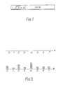
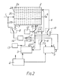
- an apparatus for use in sorting the records of Fig. 1 comprises an input data bus 1 coupled to a memory store 2 that is divided into memory storage areas having a common address, as illustrated diagrammatically by the broken lines extending vertically.
- the memory 2 has four storage areas 2A,2B,2C,2D, that are capable of being written to and read from independently of one another. It will be assumed for the purpose of the following explanation that the area 2D is to receive data corresponding to the key part of each record indicated in Fig. 1, whereas the storage area 2C is to receive the data part of the record.
- the input 1 is further connected to one pole of a change-over switch 8, the other pole of which is coupled to an output 7 from the storage area 2D of the store 2.
- An output of the switch 8 is coupled to a data selector device 14 that can, in known manner, pass, selectively, data from any one of the key fields of the record of Fig. 1.
- a counter 12 is coupled to one input of a selector switch 9 of which the output is connected to an address bus 15 of the store 2, the address presented on the bus 15 determining that address to or from which data in all sections 2A to 2D of the store is to be directed.
- a further input of the switch 9 is arranged to receive data selectively from either one of the two areas 2A and 2B of the store as described in more detail below. That output of the switch 9 coupled to the address input 15 of the store 2 is further coupled to an input of a further selector switch 16, outputs of which can be coupled selectively to either one of two further, high speed memory stores 3.
- Each store 3 is wide enough to hold the address of one location in the main store 2 and is long enough to be addressed by the data comprising one field of the key of a record as shown in Fig. 1.
- the stores 3 are fast enough to be able to perform one read and one write operation per cycle of the system, i.e. twice the speed of the main store 2.
- Address inputs of each of the stores 3 are coupled to outputs of a selector switch 11, inputs of which are coupled to an output of the data selector 14 and an output of a counter 13.
- Control inputs of each of the stores 3 are coupled to a logic device 4, which logic device is arranged to control the timing of the reading and writing operations of the stores 2 and 3 and is also arranged to control the actuation of all of the switches illustrated in Fig.
- Input records having the structure illustrated in Fig. 1 are transmitted consecutively on the data bus 1 in synchronism with the operation of the counter 12, so that consecutive records are read into the storage areas 2C and 2D at consecutive memory addresses.
- the key portion of each input record passes via the switch 8 to the data selector 14 which selects the least significant field of the key and passes this to the address input of the operative one of the high speed stores 3.
- This store initially contains in every location a bit pattern which is not a valid address in the main store.
- the high speed store location will contain the initial bit pattern, which is not a valid main store address. If one record has been read in then the location will contain the address in the main store of the record, and the storage area 2A at that address will contain the initial bit pattern.
- Each storage area 2A thus serves a pointer field indicating the preceding record with the same key value, and if two or more records have been read in then the high speed store location will contain the address of the last record, the pointer field of the last record will contain the address of the next-to-last, and so on until the earliest record will contain the initial bit pattern in its pointer field.
- This structure which is known as a linked list, is well-known in Computer Science, and is described in great detail in 'Fundamental Algorithms', by Donald Knuth.
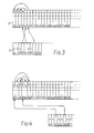
- Fig. 3 shows the position at the end of the first pass.
- List 3 contains records 4, 2 and 1
- List 4 contains record 3
- List 7 contains records 5 and 0.
- the control logic 4 When the counter 12 has generated all of the addresses of the store 2 in a first pass, assuming that the total number of records presented at input 1 corresponds to the number of addresses in the store, or when the control logic 4 detects an end of data signal at input 1, the control logic 4 now causes the switch 8 to couple the input of the data selector 14 to the output 7 of the section 2D of the store 2, while the switch 9 is coupled to link the address input 15 of the store 2 to the output of that store 3 which was in operation during the first pass.
- the input 1 to the store 2 is now inoperative so that the contents of the sections 2C and 2D of the store remain unchanged.
- the switch 11 is operated to couple the address input of the above store 3 to the output of counter 13, whilst the address input of the other store 3 is coupled to the output of data selector 14.
- the switches 16 and 10 are operated to couple the data input of the other store to the address bus 15 and the data output of the other store, via the data bus 6 to the storage area 2B of the store 2.
- the data selector 14 is also set to select the next key field of the key data taken from the storage area 2D.
- the key fields are numbered from 1 (most significant) to n (least significant). If the number of the selected key field is odd then the counter 13 is set to count up from zero to a number which represents the last address of the high speed store 3, if the number of the key field is even then the counter is set to count down from the maximum value to zero.
- the data selector 14 passes the data of the currently selected key field to the relevant high speed store 3 and data is read from and written to the latter store in the same way as in the preceding operation, i.e. the value read from the store is used to supply the address pointer to that storage area 2B of the store 2 addressed by the data bus 15, and the address on the data bus 15 is read back into high speed store 3.
- the store 3 being addressed by the counter 13 corresponds to the store 3 of Fig. 3, and as the counter 13 is incremented, original bit patterns will be output from the store 3 as the counter 13 visits the first three addresses in the store.
- the first valid address applied at address bus 15 is thus the address of record 4 of the store 2 that is contained at the address 3 of the store 3.
- the storage area 2A of address 4 of the store 2 contains the address of record 2 and so on, so that the records indicated in Fig. 3 are read in forward order and are visited in the order 4,2,1,3,5,0.
- Fig. 4 shows the corresponding position at the end of the second pass for the store 3 of which the address bus was coupled to the output of data selector 14.
- List 2 contains records 0,5,2 and 4 and List 5 contains records 3 and 1. If this is now read in reverse order the records will be visited in the order 3,1,0,5,2,4. It will be appreciated that each memory store 3 must be reset to contain the original bit pattern at all addresses before it is connected to receive the data from data selector 14 and this is achieved in an appropriate program step set by the logic device 4.
- the main store locations may be accessed in either normal or reverse order of the field which was chosen by the data selector 14 on the previous pass.
- the data will appear in an order which is the reverse of the order in which the data appeared on the previous pass. It is therefore necessary, as described above to sort into reverse order on even numbered fields, and into normal order on odd numbered fields, reflecting the number of reversals of the list which are still to come.
- Fig. 5 The process may be illustrated by the manual analogy shown in Fig. 5.
- This shows two tables A and B, on which the records may be collected in numbered piles, illustrated by the stacks of cards, representing records, shown on table B.
- the operation is continued by alternately moving the cards from table A to B and back, each time using a lower numbered field in the key.
- odd numbered field is being inspected then the cards are moving from A to B, cards are taken in descending order of pile number from A, and the cards will pass through the operator's hands in descending order of the value in the fields already used.
- even numbered field is being inspected then the cards are moving from B to A, cards are taken in ascending order of pile number from B, and cards pass through the operator's hands in ascending order of the fields already used.
- a video effects apparatus may include means for generating a series of records each comprising a data field defining the attributes of a pixel of the video image and a key field defining the position of the pixel in an image frame, means for transforming the values of the key fields of said records to define output mappings of the displacement of pixels from the input to the output picture, and a sorting apparatus as described above for sorting the transformed records into the order of said key fields to enable generation of the transformed video image frame signal by scanning of said records in the sorted order.
Landscapes
- Engineering & Computer Science (AREA)
- General Engineering & Computer Science (AREA)
- Theoretical Computer Science (AREA)
- Computer Hardware Design (AREA)
- Physics & Mathematics (AREA)
- General Physics & Mathematics (AREA)
- Information Retrieval, Db Structures And Fs Structures Therefor (AREA)
- Image Analysis (AREA)
Applications Claiming Priority (2)
| Application Number | Priority Date | Filing Date | Title |
|---|---|---|---|
| GB929207184A GB9207184D0 (en) | 1992-04-01 | 1992-04-01 | Improvements in high speed sorting |
| GB9207184 | 1992-04-01 |
Publications (3)
| Publication Number | Publication Date |
|---|---|
| EP0564290A2 true EP0564290A2 (fr) | 1993-10-06 |
| EP0564290A3 EP0564290A3 (fr) | 1993-11-03 |
| EP0564290B1 EP0564290B1 (fr) | 1996-09-04 |
Family
ID=10713290
Family Applications (1)
| Application Number | Title | Priority Date | Filing Date |
|---|---|---|---|
| EP19930302585 Expired - Lifetime EP0564290B1 (fr) | 1992-04-01 | 1993-04-01 | Appareil de triage à grande vitesse |
Country Status (3)
| Country | Link |
|---|---|
| EP (1) | EP0564290B1 (fr) |
| DE (1) | DE69304382T2 (fr) |
| GB (1) | GB9207184D0 (fr) |
Families Citing this family (1)
| Publication number | Priority date | Publication date | Assignee | Title |
|---|---|---|---|---|
| DE102010015768B4 (de) * | 2010-04-19 | 2014-11-20 | Jenoptik Katasorb Gmbh | Mikrowellenreaktor zur mikrowellenunterstützten katalytischen Stoffumsetzung |
Family Cites Families (2)
| Publication number | Priority date | Publication date | Assignee | Title |
|---|---|---|---|---|
| JPS62187977A (ja) * | 1986-02-13 | 1987-08-17 | Dainippon Screen Mfg Co Ltd | 画像デ−タ処理装置 |
| US5179717A (en) * | 1988-11-16 | 1993-01-12 | Manco, Ltd. | Sorting circuit using first and last buffer memories addressed by reference axis data and chain buffer memory addressed by datum number of the first and last buffer memories |
-
1992
- 1992-04-01 GB GB929207184A patent/GB9207184D0/en active Pending
-
1993
- 1993-04-01 EP EP19930302585 patent/EP0564290B1/fr not_active Expired - Lifetime
- 1993-04-01 DE DE1993604382 patent/DE69304382T2/de not_active Expired - Fee Related
Also Published As
| Publication number | Publication date |
|---|---|
| EP0564290B1 (fr) | 1996-09-04 |
| DE69304382D1 (de) | 1996-10-10 |
| EP0564290A3 (fr) | 1993-11-03 |
| DE69304382T2 (de) | 1997-04-03 |
| GB9207184D0 (en) | 1992-05-13 |
Similar Documents
| Publication | Publication Date | Title |
|---|---|---|
| US3938102A (en) | Method and apparatus for accessing horizontal sequences and rectangular sub-arrays from an array stored in a modified word organized random access memory system | |
| US4003024A (en) | Two-dimensional binary data enhancement system | |
| US4760526A (en) | Method for storing data into a file device and for data retrieval | |
| US3996559A (en) | Method and apparatus for accessing horizontal sequences, vertical sequences and regularly spaced rectangular subarrays from an array stored in a modified word organized random access memory system | |
| US3995253A (en) | Method and apparatus for accessing horizontal sequences, vertical sequences, and rectangular subarrays from an array stored in a modified word organized random access memory system | |
| US4903018A (en) | Process for compressing and expanding structurally associated multiple-data sequences, and arrangements for implementing the process | |
| US4561072A (en) | Memory system handling a plurality of bits as a unit to be processed | |
| US4542477A (en) | Information retrieval device | |
| EP0047782A1 (fr) | Systeme d'acces a une memoire | |
| JPH01182992A (ja) | 半導体記憶装置 | |
| US5343560A (en) | Image data display system | |
| KR920003176B1 (ko) | 정렬처리장치의 제어데이타 생성장치 | |
| EP0211385B1 (fr) | Dispositif de mémoire | |
| EP0564290B1 (fr) | Appareil de triage à grande vitesse | |
| US5008852A (en) | Parallel accessible memory device | |
| KR900008377A (ko) | 소팅 회로 | |
| US5737556A (en) | Document management system for displaying and shifting a plurality of regions | |
| EP0321493A1 (fr) | Systeme de memoire associative | |
| US5113505A (en) | Computer memory pyramidal addressing method | |
| JPH028335B2 (fr) | ||
| Gray Jr et al. | Outline for a multi-list organized system | |
| US5953454A (en) | Minimum distance storage device | |
| JPH07302187A (ja) | データソーティング方法及びソーティング装置 | |
| US5485597A (en) | A CCD array memory device achieving high speed accessing by writing and reading data through a cache memory | |
| JPS6261427A (ja) | 符号化方式 |
Legal Events
| Date | Code | Title | Description |
|---|---|---|---|
| PUAI | Public reference made under article 153(3) epc to a published international application that has entered the european phase |
Free format text: ORIGINAL CODE: 0009012 |
|
| PUAL | Search report despatched |
Free format text: ORIGINAL CODE: 0009013 |
|
| AK | Designated contracting states |
Kind code of ref document: A2 Designated state(s): DE FR GB IT |
|
| AK | Designated contracting states |
Kind code of ref document: A3 Designated state(s): DE FR GB IT |
|
| 17P | Request for examination filed |
Effective date: 19940428 |
|
| 17Q | First examination report despatched |
Effective date: 19951030 |
|
| GRAH | Despatch of communication of intention to grant a patent |
Free format text: ORIGINAL CODE: EPIDOS IGRA |
|
| GRAH | Despatch of communication of intention to grant a patent |
Free format text: ORIGINAL CODE: EPIDOS IGRA |
|
| GRAA | (expected) grant |
Free format text: ORIGINAL CODE: 0009210 |
|
| AK | Designated contracting states |
Kind code of ref document: B1 Designated state(s): DE FR GB IT |
|
| PG25 | Lapsed in a contracting state [announced via postgrant information from national office to epo] |
Ref country code: IT Free format text: LAPSE BECAUSE OF FAILURE TO SUBMIT A TRANSLATION OF THE DESCRIPTION OR TO PAY THE FEE WITHIN THE PRESCRIBED TIME-LIMIT;WARNING: LAPSES OF ITALIAN PATENTS WITH EFFECTIVE DATE BEFORE 2007 MAY HAVE OCCURRED AT ANY TIME BEFORE 2007. THE CORRECT EFFECTIVE DATE MAY BE DIFFERENT FROM THE ONE RECORDED. Effective date: 19960904 |
|
| ET | Fr: translation filed | ||
| ET1 | Fr: translation filed ** revision of the translation of the patent or the claims | ||
| REF | Corresponds to: |
Ref document number: 69304382 Country of ref document: DE Date of ref document: 19961010 |
|
| PLBE | No opposition filed within time limit |
Free format text: ORIGINAL CODE: 0009261 |
|
| STAA | Information on the status of an ep patent application or granted ep patent |
Free format text: STATUS: NO OPPOSITION FILED WITHIN TIME LIMIT |
|
| 26N | No opposition filed | ||
| PGFP | Annual fee paid to national office [announced via postgrant information from national office to epo] |
Ref country code: GB Payment date: 20000329 Year of fee payment: 8 |
|
| PGFP | Annual fee paid to national office [announced via postgrant information from national office to epo] |
Ref country code: FR Payment date: 20000407 Year of fee payment: 8 |
|
| PG25 | Lapsed in a contracting state [announced via postgrant information from national office to epo] |
Ref country code: GB Free format text: LAPSE BECAUSE OF NON-PAYMENT OF DUE FEES Effective date: 20010401 |
|
| PG25 | Lapsed in a contracting state [announced via postgrant information from national office to epo] |
Ref country code: FR Free format text: THE PATENT HAS BEEN ANNULLED BY A DECISION OF A NATIONAL AUTHORITY Effective date: 20010430 |
|
| PGFP | Annual fee paid to national office [announced via postgrant information from national office to epo] |
Ref country code: DE Payment date: 20011112 Year of fee payment: 9 |
|
| GBPC | Gb: european patent ceased through non-payment of renewal fee |
Effective date: 20010401 |
|
| REG | Reference to a national code |
Ref country code: FR Ref legal event code: ST |
|
| PG25 | Lapsed in a contracting state [announced via postgrant information from national office to epo] |
Ref country code: DE Free format text: LAPSE BECAUSE OF NON-PAYMENT OF DUE FEES Effective date: 20021101 |