EP0565116A2 - Circuit de polarisation pour une photodiode - Google Patents
Circuit de polarisation pour une photodiode Download PDFInfo
- Publication number
- EP0565116A2 EP0565116A2 EP93105866A EP93105866A EP0565116A2 EP 0565116 A2 EP0565116 A2 EP 0565116A2 EP 93105866 A EP93105866 A EP 93105866A EP 93105866 A EP93105866 A EP 93105866A EP 0565116 A2 EP0565116 A2 EP 0565116A2
- Authority
- EP
- European Patent Office
- Prior art keywords
- transistor
- load element
- circuit
- collector
- photodiode
- Prior art date
- Legal status (The legal status is an assumption and is not a legal conclusion. Google has not performed a legal analysis and makes no representation as to the accuracy of the status listed.)
- Granted
Links
Images


Classifications
-
- H—ELECTRICITY
- H04—ELECTRIC COMMUNICATION TECHNIQUE
- H04B—TRANSMISSION
- H04B10/00—Transmission systems employing electromagnetic waves other than radio-waves, e.g. infrared, visible or ultraviolet light, or employing corpuscular radiation, e.g. quantum communication
- H04B10/60—Receivers
- H04B10/66—Non-coherent receivers, e.g. using direct detection
- H04B10/69—Electrical arrangements in the receiver
- H04B10/691—Arrangements for optimizing the photodetector in the receiver
- H04B10/6911—Photodiode bias control, e.g. for compensating temperature variations
-
- G—PHYSICS
- G05—CONTROLLING; REGULATING
- G05F—SYSTEMS FOR REGULATING ELECTRIC OR MAGNETIC VARIABLES
- G05F3/00—Non-retroactive systems for regulating electric variables by using an uncontrolled element, or an uncontrolled combination of elements, such element or such combination having self-regulating properties
- G05F3/02—Regulating voltage or current
- G05F3/08—Regulating voltage or current wherein the variable is DC
- G05F3/10—Regulating voltage or current wherein the variable is DC using uncontrolled devices with non-linear characteristics
- G05F3/16—Regulating voltage or current wherein the variable is DC using uncontrolled devices with non-linear characteristics being semiconductor devices
- G05F3/20—Regulating voltage or current wherein the variable is DC using uncontrolled devices with non-linear characteristics being semiconductor devices using diode- transistor combinations
- G05F3/22—Regulating voltage or current wherein the variable is DC using uncontrolled devices with non-linear characteristics being semiconductor devices using diode- transistor combinations wherein the transistors are of the bipolar type only
- G05F3/222—Regulating voltage or current wherein the variable is DC using uncontrolled devices with non-linear characteristics being semiconductor devices using diode- transistor combinations wherein the transistors are of the bipolar type only with compensation for device parameters, e.g. Early effect, gain, manufacturing process, or external variations, e.g. temperature, loading, supply voltage
- G05F3/227—Regulating voltage or current wherein the variable is DC using uncontrolled devices with non-linear characteristics being semiconductor devices using diode- transistor combinations wherein the transistors are of the bipolar type only with compensation for device parameters, e.g. Early effect, gain, manufacturing process, or external variations, e.g. temperature, loading, supply voltage producing a current or voltage as a predetermined function of the supply voltage
-
- G—PHYSICS
- G05—CONTROLLING; REGULATING
- G05F—SYSTEMS FOR REGULATING ELECTRIC OR MAGNETIC VARIABLES
- G05F3/00—Non-retroactive systems for regulating electric variables by using an uncontrolled element, or an uncontrolled combination of elements, such element or such combination having self-regulating properties
- G05F3/02—Regulating voltage or current
- G05F3/08—Regulating voltage or current wherein the variable is DC
- G05F3/10—Regulating voltage or current wherein the variable is DC using uncontrolled devices with non-linear characteristics
- G05F3/16—Regulating voltage or current wherein the variable is DC using uncontrolled devices with non-linear characteristics being semiconductor devices
- G05F3/20—Regulating voltage or current wherein the variable is DC using uncontrolled devices with non-linear characteristics being semiconductor devices using diode- transistor combinations
- G05F3/26—Current mirrors
- G05F3/265—Current mirrors using bipolar transistors only
Definitions
- the present invention relates to a bias circuit for a photodiode and, more particularly, to a bias circuit for a photodiode, which applies a reverse voltage to the photodiode.
- V R > 0 is set to apply a reverse bias across the anode-cathode path of the photodiode 1. In this manner, the response characteristics are improved by widening the depletion layer, decreasing the junction capacitance, and strengthening the depletion layer electric field.
- the photodiode 1 is connected to one input terminal (inverting input terminal in Fig. 2) of an operational amplifier 8, and the output from the operational amplifier 8 is fed back to the input terminal (inverting input terminal) of the operational amplifier 8 via a current-voltage conversion negative feedback element 9.
- one of the anode and cathode terminals of the photodiode 1 is connected to a power supply 6 having a predetermined potential (V K ), and the other is fixed to a power supply 7 having a potential (V A ) applied to the other input terminal (non-inverting input terminal in Fig.
- a means for applying a reverse voltage across the anode-cathode path of the photodiode 1 a means using an external power supply is also available.
- a means for stacking a potential at one main voltage terminal upon combination of constant voltage elements such as diodes and a load element such as a resistor is adopted. More specifically, in Figs.
- the potential across the anode-cathode path of the photodiode 1 is determined by the constant voltage elements and the load element inserted between main voltage terminals, if the main voltage terminal defining the potential drifts in an AC manner due to the influence of, e.g., noise, a current flowing through the main voltage terminal changes.
- This problem can be solved by determining the potential across the anode-cathode path of the photodiode 1 using a constant voltage circuit having a good PSRR (power supply reduction ratio).
- PSRR power supply reduction ratio
- the present invention has been made in consideration of the conventional problems, and has as its object to suppress detection of a wrong signal and to improve signal detection precision by minimizing a change in reverse bias amount of a photodiode due to a drift of a power supply caused by, e.g., noise.
- the bias circuit is constituted by combining a current mirror circuit or a transistor, and a level shift circuit. Basically, a desired bias amount is set using the level shift circuit, and a drift of the bias amount is suppressed by the current mirror circuit or the transistor.
- a level shift circuit constituted by transistors or a combination of constant voltage elements such as diodes with a transistor, and load elements is connected to the base-collector path of a first transistor for receiving a current generated by a load element at its collector, or a second transistor, the base of which is commonly connected to the first transistor to constitute a current mirror circuit, is prepared, and the level shift circuit is connected between the base of an output transistor of the current mirror circuit and the collector of the first transistor.
- the anode or cathode of the photodiode is connected to a desired potential point of the level shift circuit to reversely bias the photodiode.
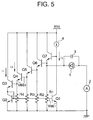
- FIG. 5 is a circuit diagram for explaining the first embodiment of the present invention.
- a circuit shown in Fig. 5 includes a photodiode 1, a current detector 2, a junction capacitance 3 of the photodiode 1, a current source 4 as a load element, a transistor Q1 (first transistor) for receiving a current supplied from the current source 4 at its collector, a transistor Q2 (second transistor), the base of which is commonly connected to the base of the transistor Q1 to constitute a current mirror circuit, and an output transistor Q3 of the current mirror circuit.
- the output transistor Q3 performs current feedback operations.
- the circuit shown in Fig. 5 includes a photodiode 1, a current detector 2, a junction capacitance 3 of the photodiode 1, a current source 4 as a load element, a transistor Q1 (first transistor) for receiving a current supplied from the current source 4 at its collector, a transistor Q2 (second transistor), the base of which is commonly connected to the base of the transistor Q1 to constitute a current mirror circuit
- level shift transistors Q4 to Q7 connected between the base of the output transistor Q3 of the current mirror circuit and the collector of the input transistor Q1 of the current mirror circuit, and load elements R1 to R4 for the level shift transistors Q4 to Q7.
- the transistor Q7 constitutes an emitter follower circuit, and is capable of cutting off a current.
- the load element 4 is an element for, e.g., generating a base voltage of the transistor Q7, and more specifically, it comprises a resistor and/or an electrical circuit.
- the load elements R1 to R4 normally comprise resistor elements.
- the transistors Q1 to Q3 have equal base-emitter voltages V BE1 .
- the level shift transistors Q4 to Q7 are driven by the predetermined load elements R1 to R4, if the load values (resistances) are set so that currents flowing through these transistors are equal to each other, these transistors can have equal base-emitter voltages V BE2 .
- a cathode potential V K of the photodiode 1 is expressed by: If a power supply V CC drifts, and consequently, the current i1 changes to change the voltages V BE1 of the transistors Q1 to Q3, a change in reverse bias amount of the photodiode 1 is given by: In this equation, since the second term is sufficiently smaller than the first term, we have: Therefore, as compared to the prior arts shown in Figs. 3 and 4, the reverse voltage drift of the photodiode 1 can be reduced. For the sake of simplicity, currents generated by the loads of the transistors Q4 to Q7 are set to be equal to each other, so that these transistors have equal base-emitter voltages. However, the base-emitter voltages may be arbitrarily determined.
- the level shift circuit may be constituted by a transistor, constant voltage elements such as diodes, and load elements.
- Fig. 6 is a circuit diagram showing the second embodiment of the present invention.
- the same reference numerals in Fig. 6 denote the same parts as in Fig 5, and a detailed description thereof will be omitted.
- level shift transistors Q10 to Q14 are connected between the base and collector of a transistor Q8 for receiving a current I1 generated by the load element 4 at its collector, and are respectively driven by load elements R5 to R9.
- the cathode current V K of the photodiode 1 is similarly expressed by: Therefore, a change in reverse bias amount of the photodiode 1 upon drift of the power supply V CC is given by: Thus, the reverse bias amount drift of the photodiode 1 can be further suppressed as compared to the first embodiment.
- Fig. 7 is a circuit diagram showing the third embodiment of the present invention.
- the same reference numerals in Fig. 7 denote the same parts as in Fig. 5, and a detailed description thereof will be omitted.
- the level shift circuit is constituted by constant voltage elements D1 to D4, a transistor Q17, and a load element R10, and is connected between the base and collector of a transistor Q15 for receiving a current generated by the load element 4 at its collector.
- the cathode potential V K of the photodiode 1 is similarly expressed by: Therefore, the reverse bias amount drift of the photodiode 1 upon drift of the power supply V CC is given by: In this manner, the drift amount can be suppressed to be equal to that in the second embodiment.
- level shift circuits shown in the first to third embodiments described above are not limited to the corresponding illustrated circuits, and may be appropriately modified within the scope of the invention. Therefore, for example, the level shift circuit of the first embodiment may be constituted by diodes.
- bias circuit for a photodiode may be modified within the spirit and scope of the invention.
- a circuit which can reduce a change in reverse bias amount of the photodiode due to a drift of a power supply caused by, e.g., noise, and can suppress generation of a wrong photoelectric current detection or signal detection signal, and/or can improve signal detection precision can be provided with a simple circuit arrangement at low cost.
- a bias circuit includes a load element (4), a transistor ((Q1) for receiving a current from the load element (4) at its collector, a transistor (Q2) constituting a current mirror circuit together with the transistor (Q1), a level shift circuit connected between the base of an output transistor (Q3) of the current mirror circuit and the collector of the transistor (Q1), and constituted by transistors (Q4 - Q7) and load elements (R1 - R4), and a photodiode (1) connected to a desired potential node of the level shift circuit.
Landscapes
- Engineering & Computer Science (AREA)
- Physics & Mathematics (AREA)
- Microelectronics & Electronic Packaging (AREA)
- Electromagnetism (AREA)
- Automation & Control Theory (AREA)
- Nonlinear Science (AREA)
- General Physics & Mathematics (AREA)
- Radar, Positioning & Navigation (AREA)
- Signal Processing (AREA)
- Computer Networks & Wireless Communication (AREA)
- Amplifiers (AREA)
- Light Receiving Elements (AREA)
- Photometry And Measurement Of Optical Pulse Characteristics (AREA)
- Electronic Switches (AREA)
Applications Claiming Priority (2)
| Application Number | Priority Date | Filing Date | Title |
|---|---|---|---|
| JP11819792A JP3207240B2 (ja) | 1992-04-10 | 1992-04-10 | フォトダイオードのバイアス回路 |
| JP118197/92 | 1992-04-10 |
Publications (3)
| Publication Number | Publication Date |
|---|---|
| EP0565116A2 true EP0565116A2 (fr) | 1993-10-13 |
| EP0565116A3 EP0565116A3 (fr) | 1993-10-20 |
| EP0565116B1 EP0565116B1 (fr) | 1997-03-12 |
Family
ID=14730580
Family Applications (1)
| Application Number | Title | Priority Date | Filing Date |
|---|---|---|---|
| EP93105866A Expired - Lifetime EP0565116B1 (fr) | 1992-04-10 | 1993-04-08 | Circuit de polarisation pour une photodiode |
Country Status (4)
| Country | Link |
|---|---|
| US (1) | US5343034A (fr) |
| EP (1) | EP0565116B1 (fr) |
| JP (1) | JP3207240B2 (fr) |
| DE (1) | DE69308615T2 (fr) |
Cited By (1)
| Publication number | Priority date | Publication date | Assignee | Title |
|---|---|---|---|---|
| EP1648101A1 (fr) * | 2004-10-15 | 2006-04-19 | Infineon Technologies Fiber Optics GmbH | Circuit de réception pour un dispositif de réception optique |
Families Citing this family (10)
| Publication number | Priority date | Publication date | Assignee | Title |
|---|---|---|---|---|
| FR2722635B1 (fr) * | 1994-07-12 | 1996-08-23 | Thomson Csf Semiconducteurs | Circuit de suppression de courant d'obscurite de photodetecteur |
| US5481104A (en) * | 1994-09-30 | 1996-01-02 | At&T Corp. | Photodetector circuit with actively damped tuned input |
| US5483182A (en) * | 1995-03-06 | 1996-01-09 | Motorola, Inc. | Method and apparatus for a DC-DC converter an current limiting thereof |
| EP1043574B1 (fr) * | 1998-10-19 | 2003-08-27 | Mitsubishi Denki Kabushiki Kaisha | Capteur infrarouge et ensemble capteur infrarouge comprenant celui-ci |
| JP4375025B2 (ja) * | 2004-01-13 | 2009-12-02 | 株式会社デンソー | 出力回路およびオペアンプ |
| GB2443204A (en) | 2006-10-04 | 2008-04-30 | Sharp Kk | Photosensor and ambient light sensor |
| JP5856391B2 (ja) | 2010-07-01 | 2016-02-09 | キヤノン株式会社 | Dc/dcコンバータ及び電子機器 |
| JP2014062839A (ja) * | 2012-09-21 | 2014-04-10 | Hamamatsu Photonics Kk | 発光検出装置 |
| JP6323921B2 (ja) * | 2016-11-08 | 2018-05-16 | Nttエレクトロニクス株式会社 | 光受信回路 |
| JP7317632B2 (ja) | 2019-08-21 | 2023-07-31 | キヤノン株式会社 | 素子、画像形成装置 |
Family Cites Families (10)
| Publication number | Priority date | Publication date | Assignee | Title |
|---|---|---|---|---|
| US3828241A (en) * | 1971-07-30 | 1974-08-06 | Sony Corp | Regulated voltage supply circuit which compensates for temperature and input voltage variations |
| JPS547181Y2 (fr) * | 1973-07-06 | 1979-04-04 | ||
| NL8100929A (nl) * | 1981-02-26 | 1982-09-16 | Philips Nv | Optische ontvanger. |
| US4759081A (en) * | 1984-04-26 | 1988-07-19 | Alcatel N.V. | Optical receiver |
| JPS6278886A (ja) * | 1985-10-01 | 1987-04-11 | Iwatsu Electric Co Ltd | アバランシエ・ホトダイオ−ドのバイアス回路 |
| JPS62159534A (ja) * | 1986-01-07 | 1987-07-15 | Omron Tateisi Electronics Co | 光送受信器 |
| FR2593319B1 (fr) * | 1986-01-17 | 1988-03-25 | Thomson Csf | Procede de lecture d'element photosensible constitue d'une photodiode et d'une capacite |
| DE3780647T2 (de) * | 1986-11-25 | 1993-03-11 | Secr Defence Brit | Quench-schaltung fuer avalanche-photodioden. |
| JPH01254080A (ja) * | 1988-04-01 | 1989-10-11 | Mitsubishi Electric Corp | 光電変換アンプ |
| US5270533A (en) * | 1992-06-23 | 1993-12-14 | Smiths Industries | Stabilization biasing circuit for avalanche photodiodes |
-
1992
- 1992-04-10 JP JP11819792A patent/JP3207240B2/ja not_active Expired - Fee Related
-
1993
- 1993-04-08 DE DE69308615T patent/DE69308615T2/de not_active Expired - Lifetime
- 1993-04-08 EP EP93105866A patent/EP0565116B1/fr not_active Expired - Lifetime
- 1993-04-08 US US08/043,932 patent/US5343034A/en not_active Expired - Lifetime
Cited By (1)
| Publication number | Priority date | Publication date | Assignee | Title |
|---|---|---|---|---|
| EP1648101A1 (fr) * | 2004-10-15 | 2006-04-19 | Infineon Technologies Fiber Optics GmbH | Circuit de réception pour un dispositif de réception optique |
Also Published As
| Publication number | Publication date |
|---|---|
| DE69308615D1 (de) | 1997-04-17 |
| JP3207240B2 (ja) | 2001-09-10 |
| US5343034A (en) | 1994-08-30 |
| EP0565116A3 (fr) | 1993-10-20 |
| JPH05288605A (ja) | 1993-11-02 |
| DE69308615T2 (de) | 1997-07-31 |
| EP0565116B1 (fr) | 1997-03-12 |
Similar Documents
| Publication | Publication Date | Title |
|---|---|---|
| EP0072589B1 (fr) | Dispositif de stabilisation de courant | |
| EP0565116B1 (fr) | Circuit de polarisation pour une photodiode | |
| US4578633A (en) | Constant current source circuit | |
| US4485301A (en) | Linear two-terminal integrated circuit photo sensor | |
| US4362956A (en) | Absolute value circuit | |
| KR830001456B1 (ko) | 전력트랜지스터용 과전류 보호회로 | |
| EP0039178B1 (fr) | Circuit intégré pour engendrer une tension de référence | |
| JP3335754B2 (ja) | 定電圧発生回路 | |
| US3714543A (en) | Constant current circuit constituted on a monolithic ic | |
| US4490669A (en) | Circuit configuration for generating a temperature-independent reference voltage | |
| KR920009548B1 (ko) | 전류원 장치 | |
| US4216394A (en) | Leakage current compensation circuit | |
| GB2120486A (en) | High input impedance circuits | |
| US4571536A (en) | Semiconductor voltage supply circuit having constant output voltage characteristic | |
| US4103220A (en) | Low dissipation voltage regulator | |
| EP0110720B1 (fr) | Circuit à miroir de courant | |
| US4177416A (en) | Monolithic current supplies having high output impedances | |
| CA1301862C (fr) | Circuit d'amplificatin logarithmique fournissant une tension de sortie correspondant a la difference des valeurs amplifiees logarithmiquement de deux cournants d'entree | |
| US4117391A (en) | Current stabilizing circuit | |
| US5973314A (en) | Photoelectric converting device which prevents power source ripple from mixing into an output signal | |
| EP0290277B1 (fr) | Circuit de charge actif intégré à faible bruit | |
| KR100228354B1 (ko) | 전원전압 및 온도변화에 무관한 기준전압 발생기 | |
| KR830000542B1 (ko) | 이득 제어회로 | |
| US4230980A (en) | Bias circuit | |
| SU1480094A1 (ru) | Выходной каскад операционного усилител |
Legal Events
| Date | Code | Title | Description |
|---|---|---|---|
| PUAI | Public reference made under article 153(3) epc to a published international application that has entered the european phase |
Free format text: ORIGINAL CODE: 0009012 |
|
| PUAL | Search report despatched |
Free format text: ORIGINAL CODE: 0009013 |
|
| AK | Designated contracting states |
Kind code of ref document: A2 Designated state(s): DE FR GB |
|
| AK | Designated contracting states |
Kind code of ref document: A3 Designated state(s): DE FR GB |
|
| RHK1 | Main classification (correction) |
Ipc: G05F 3/22 |
|
| 17P | Request for examination filed |
Effective date: 19940302 |
|
| 17Q | First examination report despatched |
Effective date: 19950524 |
|
| GRAG | Despatch of communication of intention to grant |
Free format text: ORIGINAL CODE: EPIDOS AGRA |
|
| GRAH | Despatch of communication of intention to grant a patent |
Free format text: ORIGINAL CODE: EPIDOS IGRA |
|
| GRAH | Despatch of communication of intention to grant a patent |
Free format text: ORIGINAL CODE: EPIDOS IGRA |
|
| GRAA | (expected) grant |
Free format text: ORIGINAL CODE: 0009210 |
|
| AK | Designated contracting states |
Kind code of ref document: B1 Designated state(s): DE FR GB |
|
| REF | Corresponds to: |
Ref document number: 69308615 Country of ref document: DE Date of ref document: 19970417 |
|
| ET | Fr: translation filed | ||
| PLBE | No opposition filed within time limit |
Free format text: ORIGINAL CODE: 0009261 |
|
| 26N | No opposition filed | ||
| REG | Reference to a national code |
Ref country code: GB Ref legal event code: IF02 |
|
| PGFP | Annual fee paid to national office [announced via postgrant information from national office to epo] |
Ref country code: FR Payment date: 20090424 Year of fee payment: 17 |
|
| REG | Reference to a national code |
Ref country code: FR Ref legal event code: ST Effective date: 20101230 |
|
| PG25 | Lapsed in a contracting state [announced via postgrant information from national office to epo] |
Ref country code: FR Free format text: LAPSE BECAUSE OF NON-PAYMENT OF DUE FEES Effective date: 20100430 |
|
| PGFP | Annual fee paid to national office [announced via postgrant information from national office to epo] |
Ref country code: DE Payment date: 20110430 Year of fee payment: 19 |
|
| PGFP | Annual fee paid to national office [announced via postgrant information from national office to epo] |
Ref country code: GB Payment date: 20110413 Year of fee payment: 19 |
|
| GBPC | Gb: european patent ceased through non-payment of renewal fee |
Effective date: 20120408 |
|
| PG25 | Lapsed in a contracting state [announced via postgrant information from national office to epo] |
Ref country code: GB Free format text: LAPSE BECAUSE OF NON-PAYMENT OF DUE FEES Effective date: 20120408 |
|
| REG | Reference to a national code |
Ref country code: DE Ref legal event code: R119 Ref document number: 69308615 Country of ref document: DE Effective date: 20121101 |
|
| PG25 | Lapsed in a contracting state [announced via postgrant information from national office to epo] |
Ref country code: DE Free format text: LAPSE BECAUSE OF NON-PAYMENT OF DUE FEES Effective date: 20121101 |