EP0565227B1 - Microscope à balayage à force atomique - Google Patents
Microscope à balayage à force atomique Download PDFInfo
- Publication number
- EP0565227B1 EP0565227B1 EP93301417A EP93301417A EP0565227B1 EP 0565227 B1 EP0565227 B1 EP 0565227B1 EP 93301417 A EP93301417 A EP 93301417A EP 93301417 A EP93301417 A EP 93301417A EP 0565227 B1 EP0565227 B1 EP 0565227B1
- Authority
- EP
- European Patent Office
- Prior art keywords
- scanning
- force microscope
- specimen
- lever arm
- optical lever
- Prior art date
- Legal status (The legal status is an assumption and is not a legal conclusion. Google has not performed a legal analysis and makes no representation as to the accuracy of the status listed.)
- Expired - Lifetime
Links
- 239000000523 sample Substances 0.000 claims description 57
- 230000003287 optical effect Effects 0.000 claims description 37
- 239000000758 substrate Substances 0.000 claims description 10
- 229910000831 Steel Inorganic materials 0.000 claims description 4
- 239000010959 steel Substances 0.000 claims description 4
- 238000013459 approach Methods 0.000 description 10
- 239000007788 liquid Substances 0.000 description 7
- 239000012530 fluid Substances 0.000 description 5
- 239000004593 Epoxy Substances 0.000 description 4
- 239000000919 ceramic Substances 0.000 description 4
- 239000006091 Macor Substances 0.000 description 3
- 238000013461 design Methods 0.000 description 3
- 239000000463 material Substances 0.000 description 3
- 238000000034 method Methods 0.000 description 3
- 230000004044 response Effects 0.000 description 3
- LFQSCWFLJHTTHZ-UHFFFAOYSA-N Ethanol Chemical compound CCO LFQSCWFLJHTTHZ-UHFFFAOYSA-N 0.000 description 2
- 229910052581 Si3N4 Inorganic materials 0.000 description 2
- 239000000853 adhesive Substances 0.000 description 2
- 230000001070 adhesive effect Effects 0.000 description 2
- 230000000694 effects Effects 0.000 description 2
- 238000003384 imaging method Methods 0.000 description 2
- 230000007246 mechanism Effects 0.000 description 2
- 229920000642 polymer Polymers 0.000 description 2
- 230000008569 process Effects 0.000 description 2
- HQVNEWCFYHHQES-UHFFFAOYSA-N silicon nitride Chemical compound N12[Si]34N5[Si]62N3[Si]51N64 HQVNEWCFYHHQES-UHFFFAOYSA-N 0.000 description 2
- 230000008859 change Effects 0.000 description 1
- 230000006835 compression Effects 0.000 description 1
- 238000007906 compression Methods 0.000 description 1
- 230000003247 decreasing effect Effects 0.000 description 1
- 230000001419 dependent effect Effects 0.000 description 1
- 238000005530 etching Methods 0.000 description 1
- 239000011521 glass Substances 0.000 description 1
- 238000005286 illumination Methods 0.000 description 1
- 238000003754 machining Methods 0.000 description 1
- 238000004519 manufacturing process Methods 0.000 description 1
- 238000012986 modification Methods 0.000 description 1
- 230000004048 modification Effects 0.000 description 1
- 238000002360 preparation method Methods 0.000 description 1
- 238000001314 profilometry Methods 0.000 description 1
- BDERNNFJNOPAEC-UHFFFAOYSA-N propan-1-ol Chemical compound CCCO BDERNNFJNOPAEC-UHFFFAOYSA-N 0.000 description 1
- 238000012552 review Methods 0.000 description 1
- 229910052710 silicon Inorganic materials 0.000 description 1
- 239000010703 silicon Substances 0.000 description 1
- 230000005641 tunneling Effects 0.000 description 1
- XLYOFNOQVPJJNP-UHFFFAOYSA-N water Substances O XLYOFNOQVPJJNP-UHFFFAOYSA-N 0.000 description 1
Images


Classifications
-
- G—PHYSICS
- G01—MEASURING; TESTING
- G01Q—SCANNING-PROBE TECHNIQUES OR APPARATUS; APPLICATIONS OF SCANNING-PROBE TECHNIQUES, e.g. SCANNING PROBE MICROSCOPY [SPM]
- G01Q30/00—Auxiliary means serving to assist or improve the scanning probe techniques or apparatus, e.g. display or data processing devices
- G01Q30/08—Means for establishing or regulating a desired environmental condition within a sample chamber
-
- B—PERFORMING OPERATIONS; TRANSPORTING
- B82—NANOTECHNOLOGY
- B82Y—SPECIFIC USES OR APPLICATIONS OF NANOSTRUCTURES; MEASUREMENT OR ANALYSIS OF NANOSTRUCTURES; MANUFACTURE OR TREATMENT OF NANOSTRUCTURES
- B82Y35/00—Methods or apparatus for measurement or analysis of nanostructures
-
- G—PHYSICS
- G01—MEASURING; TESTING
- G01Q—SCANNING-PROBE TECHNIQUES OR APPARATUS; APPLICATIONS OF SCANNING-PROBE TECHNIQUES, e.g. SCANNING PROBE MICROSCOPY [SPM]
- G01Q20/00—Monitoring the movement or position of the probe
- G01Q20/02—Monitoring the movement or position of the probe by optical means
-
- G—PHYSICS
- G01—MEASURING; TESTING
- G01Q—SCANNING-PROBE TECHNIQUES OR APPARATUS; APPLICATIONS OF SCANNING-PROBE TECHNIQUES, e.g. SCANNING PROBE MICROSCOPY [SPM]
- G01Q30/00—Auxiliary means serving to assist or improve the scanning probe techniques or apparatus, e.g. display or data processing devices
- G01Q30/08—Means for establishing or regulating a desired environmental condition within a sample chamber
- G01Q30/12—Fluid environment
- G01Q30/14—Liquid environment
-
- G—PHYSICS
- G01—MEASURING; TESTING
- G01Q—SCANNING-PROBE TECHNIQUES OR APPARATUS; APPLICATIONS OF SCANNING-PROBE TECHNIQUES, e.g. SCANNING PROBE MICROSCOPY [SPM]
- G01Q70/00—General aspects of SPM probes, their manufacture or their related instrumentation, insofar as they are not specially adapted to a single SPM technique covered by group G01Q60/00
- G01Q70/02—Probe holders
-
- Y—GENERAL TAGGING OF NEW TECHNOLOGICAL DEVELOPMENTS; GENERAL TAGGING OF CROSS-SECTIONAL TECHNOLOGIES SPANNING OVER SEVERAL SECTIONS OF THE IPC; TECHNICAL SUBJECTS COVERED BY FORMER USPC CROSS-REFERENCE ART COLLECTIONS [XRACs] AND DIGESTS
- Y10—TECHNICAL SUBJECTS COVERED BY FORMER USPC
- Y10S—TECHNICAL SUBJECTS COVERED BY FORMER USPC CROSS-REFERENCE ART COLLECTIONS [XRACs] AND DIGESTS
- Y10S977/00—Nanotechnology
- Y10S977/84—Manufacture, treatment, or detection of nanostructure
- Y10S977/849—Manufacture, treatment, or detection of nanostructure with scanning probe
- Y10S977/86—Scanning probe structure
- Y10S977/868—Scanning probe structure with optical means
- Y10S977/87—Optical lever arm for reflecting light
Definitions
- This invention relates generally to scanning force microscopes, and more particularly concerns a sensor module for a scanning force microscope with integrated scanning drivers for use with a stationary specimen.
- Scanning force microscopes also known as atomic force microscopes, are useful for imaging objects as small as atoms.
- the scanning force microscope is closely related to the scanning tunneling microscope and the technique of stylus profilometry, however in a typical scanning force microscope, deflection of a laser beam by a vertical movement of a probe following the contours of a specimen is amplified by a reflective lever arm to which the probe is mounted.
- the deflection of the laser beam is typically monitored by a photodetector in the optical path of the deflected laser beam, and the sample is mounted on a stage moveable in minute distances in three dimensions so that the sample can be raster scanned while the vertical positioning of the probe relative to the surface of the sample is maintained substantially constant by a feedback loop with the photodetector controlling the vertical positioning of the sample.
- Such scanning force microscopes are useful for imaging a sample which is moved in three dimensions while the sensor head is stationary and separate from the scanning assembly moving the sample.
- this conventional design is only useful for samples which are comparatively small or which can be cut small enough from a larger specimen to be examined on the scanning stage of the microscope.
- Such samples typically must also weigh about a gram or less, in order to accommodate the relatively high scan rates without causing distortion due to resonance effects.
- Various designs of free standing scanning force microscopes which include a scanning mechanism and sensor element for scanning large samples are also known and described, for example in US-A-5,025,658.
- a probe In conventional scanning force microscopes, a probe can also be damaged by too abrupt an approach to a sample before feedback position control of the sensor head is actually engaged. The user typically cannot easily view the approach of the lever arm and probe assembly to the surface of the sample to insure precise positioning of the probe. Even where an optical microscope is used in conjunction with the scanning force microscope to view the sample, the arrangement of the optical microscope with the scanning force microscope can be inconvenient and clumsy, and can interfere with the operation of the scanning force microscope. It would further be desirable to provide the base of the microscope with motorized driver means for operating the approach of the optical lever arm and sensor head to the sample, which can be controlled by feedback control means, to allow the process of approach of the sensor head to the sample to be automated.
- embodiments of the present invention provide for an improved free standing type of scanning force microscope with integrated scanning drivers for examination of an extremely wide range of sizes and weights of stationary specimens, with the capability of scanning a sample in contact with a fluid, and with motorized driver means for operating the approach of the optical lever arm and sensor head to the sample, to allow for automation of the approach of the sensor head to the specimen.
- the present invention provides a scanning force microscope for examining surface contours of a stationary specimen, the scanning force microscope comprising:
- Means for viewing the optical lever arm, probe means, and an adjacent specimen may also be provided.
- the optical lever arm means preferably includes a reflective cantilever arm having a free end to which the probe tip is mounted, and the optical lever arm means is preferably magnetically secured to the body.
- the photodetector means preferably includes a photodetector mounted to the body, and mirror means mounted within the body to deflect the laser beam from the optical lever arm means to the photodetector.
- the microscope includes a sealed window which may be placed in a liquid containing the specimen for examining the specimen in a liquid environment.
- Scanning force microscopes are typically limited for use with comparatively small samples of a gram or less, to accommodate scan rates of such microscopes without causing distortion due to resonance effects.
- Free standing type scanning force microscopes are frequently difficult to operate and employ a sensor head force on a sample which prohibits examination of many polymers and biological molecules.
- Such microscopes typically also do not include the capability of scanning a sample in a liquid environment, limiting the quality and opportunities for viewing of specimens.
- Scanning force microscopes also commonly do not allow for feedback control of the approach of the lever arm and probe assembly to the surface of the sample to insure precise positioning of the probe, allowing a probe to be damaged by too abrupt an approach.
- an improved free standing type scanning force microscope 10 having a stationary body 12 including a lower base 14 secured to the body by screws or bolts, with adjustable motor driven legs 16a,b,c for supporting the body of the microscope on a substrate 13 and moving the body of the microscope in a vertical dimension relative to a specimen 18 mounted with respect to the substrate.
- Each of the motor driven legs includes an optically encoded screw drive motor 17 connected to a control unit, as is described later, which coordinates the operation of the legs in response to position signals from the optically encoded screw drive motors, so that the motors operate in unison to raise and lower the microscope uniformly.
- the specimen to be examined can in fact consist of a portion of the substrate, and can therefore in principle be of any size or weight, such as the wing of an aircraft, or a desk top, for example.
- the base of the microscope typically has the general shape of a rectangular block, and preferably includes a middle bore 20 for extension of the sensor head to the specimen to be examined, and for the light path of laser beam to optical lever arm of the sensor head, as will be explained further.
- the motorized adjustable support legs 16a,b,c of the base are preferably three in number, arranged in a tripod, although other numbers of support legs such as four, for example, arranged at the corners of the rectangular base may also be possible.
- the length of extension of the support legs from the bottom of the base is preferably adjustable by screw drive motors 17a,b,c to which the support legs are mounted, and the screw drive motors are typically mounted to the upper side of the base with the support legs extending through bores in the base.
- the rectangular block of the base may also include a bore 24 for an objective lens 25 or charge couple device (not shown) extending through the block and focusing on the area where the optical lever arm, sensor head and surface of the specimen will come together.
- a second bore 26 may also be provided through the base, also directed to the area of the optical lever arm and specimen, to allow illumination to be directed from a lamp 27, for example, to this area for optically viewing the approach of the sensor head to the specimen.
- a scanner assembly shell 28 having lower legs is preferably mounted to the upper side of the base at leg attachment sites. The upper end of the scanner shell assembly provides a site for mounting the pivot 34 for the body of the generally cylindrical inner sensor assembly or kernel 35, which includes the laser light source and sensor head assembly 36.
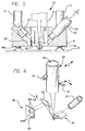
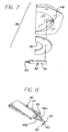
- the sensor head assembly 36 preferably includes an optical lever arm 40 secured to the body of the inner sensor assembly as will be further explained below, and preferably includes a half washer member 42 of magnetic steel, magnetically secured to a magnet 44 secured to the body of the inner sensor assembly.
- An integral cantilever support member 45 is mounted to a central portion of the half washer member, extending to the open middle portion of the half washer member.
- a reflective cantilever arm 46 formed in the shape of a triangle from first and second arms 48a, 48b is secured at one end to the free end 47 of the integral cantilever support member and joined together at their free ends 50.
- the arms of the cantilever arm are typically about 18 microns wide, about 200 microns long, about 0.6 microns thick, and are secured to the integral cantilever support member about 120 microns apart.
- silicon nitride material available from Park Scientific Instruments
- the cantilever arm bows and flexes as much as 20° in response to the force of the probe tip against the specimen, amplifying the deflection of the laser beam, as will be explained further below.
- the integral cantilever support member and the reflective cantilever arm are so small that they are most conveniently etched from silicon nitride, although other materials such as silicon which can lend themselves to etching, fine machining, or other such processes familiar to those skilled in the art of manufacturing integrated circuit chips, and which can provide a reflective surface may be suitable as well.
- Attached to the free end 50 of the cantilever arm is a probe means 60 including a distal needle-like probe tip 62 adapted to contact and follow the surface contours of the specimen.
- a laser light source means 70 such as a laser diode with associated optics, is mounted in the upper portion of the body for producing a focused laser beam 72 directed at and deflected by the reflective cantilever arm.
- a laser diode which is commercially available is a 3 milliwatt laser diode which produces a beam in the 670 nm range.
- An opening is provided in the removable base to allow the laser beam to pass through to the cantilever arm.
- three or more adjustment screws 74 for adjusting the alignment and aiming of the laser light source are mounted in threaded access ports provided in the body.
- a reflective means such as the planar mirror 80 is preferably mounted in the interior of the body at a distal end of an adjustment screw 82 through threaded access port 84 to reflect the deflected beam 86 to a photodetector 88 mounted to the body for receiving the deflected laser beam.
- the photodetector preferably generates an electrical output signal in response to the deflected laser beam indicative of the degree of deflection of the laser beam by the cantilever arm.
- the photodetector is mounted to receive the deflected laser beam through photodetector port 94 in the body, and is typically formed as an array of four photosensors 90, in which the top pair 92a is coupled to provide a combined signal, and the bottom pair 92b is coupled to provide a combined signal.
- the deflected laser beam is typically targeted at a central point between the top and bottom portions of the photodetector, and the combined signals from these portions are processed to generate output signals which can be compared to produce a differential error signal by control means 110.
- the mechanism for raster scanning the sensor head preferably includes a pair of stacked piezo drivers 100 disposed in the scanner shell assembly oriented horizontally at right angles to each other for low resolution or large scale x and y raster scanning movements ranging approximately from zero to 200 microns, and corresponding opposing coil compression springs 102.
- the large motion horizontal piezo drivers 100 and the opposing coil springs are mounted between the inner scanner assembly and the scanner shell in push rods 96 having push rod chambers for containing and securing one end of the piezo drivers and springs.
- a stacked piezo driver 104 mounted vertically in a holder 106 preferably formed of an insulating ceramic such as that sold under the trade name MACOR, available from Corning, mounted, for example by an adhesive such as epoxy, in a portion of a piezo tube driver 108, of the type which is well known in the art.
- the upper end of the piezo driver 104 is preferably adhesively secured to the holder such as by epoxy, and the lower end of the piezo driver 104 is preferably adhesively secured, such as by epoxy 107 to a sensor head mounting block 109, preferably formed of an insulating ceramic such as MACOR, to which the magnet of the sensor head assembly is secured.
- the range of motion of the stacked piezo drivers is of course dependent upon the piezo material selected and the length of the piezo stack.
- the piezo tube driver 108 is mounted to the lower end of the body of the inner sensor assembly, to provide for small scale x, y, and z motion of sensor head assembly.
- the small scale motion achievable with the piezo tube driver ranges approximately from zero to 5 microns in the vertical or z direction, and approximately from zero to 10 microns in the horizontal or x and y dimensions, depending upon the size of the cantilever arms of the sensor head assembly, typically with an atomic resolution as small as approximately .02 nm in the vertical dimension, and approximately .03 nm in the horizontal dimension.
- the scanning means preferably also includes feedback control means 110 for driving the piezo tube in the vertical dimension as the probe tip traverses the contours of the specimen, to maintain a substantially constant force of the probe means against the surface of the specimen.
- the control means preferably comprises microprocessor means electrically connected to the photodetector means by line 113 to receive the output signals indicative of deflection of the laser beam from the optical lever arm means, and for generating the error signal indicative of a variance from the constant amount of force of the probe tip against the specimen surface.
- the control means is electrically connected to the piezoelectric drivers by control lines 114a-c for raising and lowering the sensor head assembly with respect to the specimen for increasing or decreasing the force of the probe tip against the specimen surface to maintain the substantially constant amount of force of the probe tip against the specimen surface, and for raster scanning the sensor head assembly in a horizontal plane in X and Y directions.
- the optically encoded screw drive motors 17 of the motor driven legs are also connected to the control means 110 by control lines 116 enabling the control means to receive the optically encoded position signals from the drive motors and to uniformly coordinate the operation of the drive motors in raising and lowering the microscope.
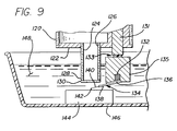
- the tubular piezo ceramic tube driver 120 is fitted with an end piece or cap 122 having a middle viewing tube 124 secured to the cap at an upper end 126 of the viewing tube and extending downwardly therefrom.
- the viewing tube is sealed at its lower end 128 by a window 130 such as a thin plate of glass, to allow the piezo tube to be placed in a liquid.
- a stacked piezo driver 131 is secured to the piezo tube for large vertical movements of the sensor head assembly, and adhesively secured at 133 to the lower end of the piezo driver, by an adhesive such as epoxy, is a sensor head mounting block 135, preferably formed of an insulating ceramic such as MACOR.
- the mounting block contains magnet holder 132, to which the optical lever arm 134 is preferably magnetically secured, as in the previous embodiment.
- a half washer member 136 made of magnetic steel is magnetically secured to the magnet, and an integral cantilever support member 138 extends from the middle of the half washer member to support the cantilever arm 140.
- the probe tip 142 extends from the underside of the cantilever arm, to be placed in contact with a specimen 144, preferably mounted on substrate 146 in a liquid environment 148 such as water, propanol, ethanol, or the like.
- the remainder of the structure of the scanning force microscope in this alternate embodiment is substantially identical to that of the previous embodiment.
- the sensor head assembly can thus be submerged in the liquid environment for scanning of the stationary specimen.
- the scanning force microscope described provides for an improved mount for the probe of the microscope, which is easier to handle and install in the microscope.
- the integrated optics of the microscope permits the user to view the approach of the lever arm and probe assembly to the surface of the sample to insure safe and precise positioning of the probe near the specimen.
- the scanning force microscope also includes the capability of scanning a specimen in a fluid environment, which can significantly improve the quality of the image of the specimen produced by the instrument.
Landscapes
- Physics & Mathematics (AREA)
- Health & Medical Sciences (AREA)
- General Health & Medical Sciences (AREA)
- General Physics & Mathematics (AREA)
- Nuclear Medicine, Radiotherapy & Molecular Imaging (AREA)
- Radiology & Medical Imaging (AREA)
- Chemical & Material Sciences (AREA)
- Engineering & Computer Science (AREA)
- Nanotechnology (AREA)
- Analytical Chemistry (AREA)
- Crystallography & Structural Chemistry (AREA)
- Length Measuring Devices With Unspecified Measuring Means (AREA)
Claims (16)
- Microscope (10) à balayage à force atomique pour l'examen des contours de surface d'un échantillon immobile (18), le microscope (10) à balayage à force atomique comportant :un corps (28) ayant une base (14) conçue pour être positionnée sur un substrat (13) par rapport audit échantillon (18) et comprenant un pivot (34) pour le montage pivotant d'un coeur (35) par rapport audit corps (28) ;un moyen capteur (36) monté sur ledit coeur (35) pour se déplacer par rapport audit corps (28), ledit moyen capteur (36) comprenant un moyen à bras de levier optique (40) ayant une surface réfléchissante (46) et une pointe de sonde (62) reliée audit moyen à bras de levier optique (40), ladite pointe de sonde (62) étant conçue pour entrer en contact avec les contours de surface de l'échantillon (18) et les suivre sous une force d'une amplitude sensiblement constante ;un moyen (70) à source de lumière laser monté sur ledit coeur (35) pour produire un faisceau laser focalisé (72) dirigé sur ledit moyen (40) à bras de levier optique et dévié par celui-ci ;un moyen photodétecteur (88) destiné à recevoir ledit faisceau laser (86) dévié par ledit moyen à bras de levier optique (40) et à générer un signal de sortie représentatif de degré de déviation dudit faisceau laser (86) par ledit moyen à bras de levier optique (40), ledit moyen photodétecteur (88) étant monté sur ledit coeur (35) ;des moyens de balayage à grande échelle (100, 102, 104) destinés à faire pivoter ledit coeur (35) pour produire un mouvement de balayage tramé X et Y par rapport audit échantillon (18) et pour déplacer ledit moyen à bras de levier optique (40) dans une dimension Z indépendamment de tous mouvements de balayage tramés X et Y ;un moyen (108) de balayage à petite échelle pour déplacer ledit moyen capteur (36) par rapport audit coeur (35) et audit échantillon (18) dans trois degrés de liberté ; etun moyen de commande (110) destiné à maintenir une force constante de ladite pointe de sonde (62) contre lesdits contours de surface dudit échantillon (18).
- Microscope (10) à balayage à force atomique selon la revendication 1, dans lequel ledit moyen à bras de levier optique (40) comprend un bras fléchissant en porte-à-faux (46) ayant une extrémité libre (50).
- Microscope (10) à balayage à force atomique selon la revendication 2, dans lequel ladite pointe de sonde (62) est montée sur ladite extrémité libre (50) dudit bras en porte-à-faux (46).
- Microscope (10) à balayage à force atomique selon la revendication 1, dans lequel ledit moyen à bras de levier optique (40) comprend une extrémité libre (50) et ladite pointe de sonde (62) est montée sur ladite extrémité libre (50) dudit moyen à bras de levier optique (40).
- Microscope (10) à balayage à force atomique selon l'une quelconque des revendications précédentes, dans lequel ledit moyen à bras de levier optique (40) est fixé magnétiquement audit moyen capteur (36).
- Microscope (10) à balayage à force atomique selon la revendication 5, dans lequel ledit moyen capteur (36) comprend une partie magnétique (44), ledit moyen à bras de levier optique (40) comprend un élément en acier magnétique (42) fixé magnétiquement à ladite partie magnétique (44) dudit moyen capteur (36), et ledit bras en porte-à-faux (46) est monté sur ledit élément en acier magnétique (42).
- Microscope (10) à balayage à force atomique selon l'une quelconque des revendications précédentes, dans lequel ledit moyen photodécteur (88) comprend un photodétecteur (88) monté sur ledit coeur (35), et comprend en outre un moyen réfléchissant (80) monté à l'intérieur dudit coeur (35) pour dévier ledit faisceau laser (86) depuis ledit moyen à bras de levier optique (40) vers ledit photodétecteur (88).
- Microscope (10) à balayage à force atomique selon l'une quelconque des revendications précédentes, dans lequel ledit moyen (100, 102) de balayage à grande échelle comprend plusieurs éléments piézoélectriques d'attaque disposés de façon à être adjacents audit corps (28) et reliés fonctionnellement audit moyen de commande (110) pour faire pivoter ledit coeur (35) afin de produire un mouvement de balayage tramé X et Y par rapport auxdits contours de surface dudit échantillon (18).
- Microscope (10) à balayage à force atomique selon l'une quelconque des revendications précédentes, dans lequel ledit corps (28) comprend des moyens (16a, b, c) destinés à régler la distance de ladite base (14) par rapport audit substrat (13).
- Microscope (10) à balayage à force atomique selon la revendication 9, dans lequel lesdits moyens de réglage de distance (16a, b, c) comprennent plusieurs éléments à pieds réglables (16a, b, c) montés sur ladite base (14) et conçus pour entrer en contact avec ledit substrat (13), et un moyen (17) d'entraínement des éléments à pieds relié auxdits éléments à pieds (16a, b, c) et audit corps (28) pour allonger et rétracter individuellement lesdits plusieurs éléments à pieds (16a, b, c) par rapport à ladite base (14), ledit moyen (17) d'entraínement des éléments à pieds étant relié fonctionnellement audit moyen de commande (110).
- Microscope (10) à balayage à force atomique selon la revendication 10, dans lequel ledit moyen (17) d'entraínement des éléments à pieds comporte plusieurs moteurs correspondants (17) d'entraínement à vis codés optiquement associés auxdits éléments associés (16a, b, c) et montés sur ladite base (14) pour entraíner lesdits éléments à pieds (16a, b, c) afin de faire monter et descendre le microscope (10), lesdits moteurs d'entraínement (17) étant conçus pour générer le signal de position indicatif d'une position des éléments à pieds associés (16a, b, c), ledit moyen de commande (110) étant relié auxdits plusieurs moteurs d'entraínement (17) pour recevoir ledit signal de position et pour commander l'action desdits moteurs d'entraínement (17) afin de faire monter et descendre uniformément ledit microscope (10) par rapport audit substrat (13).
- Microscope (10) à balayage à force atomique selon l'une quelconque des revendications précédentes, dans lequel ledit moyen de commande (110) comprend un moyen relié audit moyen photodétecteur (88) pour recevoir ledit signal de sortie indicatif d'une déviation du faisceau laser (86) à partir dudit moyen à bras de levier optique (40), un moyen destiné à générer un signal d'erreur indicatif d'une variation à partir de ladite force d'amplitude constante de ladite pointe de sonde (62) contre ladite surface de l'échantillon, et un moyen d'attaque électrique (104) qui, en réponse audit signal d'erreur, est destiné à faire monter et descendre ladite pointe de sonde (62) par rapport audit échantillon (18) afin d'augmenter ou de diminuer la force de ladite pointe de sonde (62) contre ladite surface de l'échantillon pour maintenir ladite force d'amplitude sensiblement constante de ladite pointe de sonde (62) contre ladite surface de l'échantillon.
- Microscope (10) à balayage à force atomique selon l'une quelconque des revendications précédentes, dans lequel ladite base (14) comprend une chambre destinée à recevoir ledit échantillon (18).
- Microscope (10) à balayage à force atomique selon la revendication 1, dans lequel ledit moyen de balayage (100, 102) à grande échelle balaie ladite pointe de sonde (62) par rapport audit échantillon (18) en mouvements de balayage tramés X et Y couvrant approximativement 0 à 200 micromètres.
- Microscope (10) à balayage à force atomique selon la revendication 1, dans lequel ledit moyen (104) de balayage à grande échelle déplace ledit moyen à bras de levier optique (40) dans une dimension Z d'environ 0 à 20 micromètres indépendamment desdits mouvements de balayage tramés X et Y.
- Microscope (10) à balayage à force atomique selon la revendication 1, dans lequel la partie de base (122) dudit coeur (35) comporte une fenêtre d'observation (130) scellée de façon étanche.
Applications Claiming Priority (2)
| Application Number | Priority Date | Filing Date | Title |
|---|---|---|---|
| US847160 | 1992-03-06 | ||
| US07/847,160 US5319960A (en) | 1992-03-06 | 1992-03-06 | Scanning force microscope |
Publications (2)
| Publication Number | Publication Date |
|---|---|
| EP0565227A1 EP0565227A1 (fr) | 1993-10-13 |
| EP0565227B1 true EP0565227B1 (fr) | 1999-06-23 |
Family
ID=25299925
Family Applications (1)
| Application Number | Title | Priority Date | Filing Date |
|---|---|---|---|
| EP93301417A Expired - Lifetime EP0565227B1 (fr) | 1992-03-06 | 1993-02-25 | Microscope à balayage à force atomique |
Country Status (4)
| Country | Link |
|---|---|
| US (1) | US5319960A (fr) |
| EP (1) | EP0565227B1 (fr) |
| JP (1) | JPH0626854A (fr) |
| DE (1) | DE69325409T2 (fr) |
Families Citing this family (41)
| Publication number | Priority date | Publication date | Assignee | Title |
|---|---|---|---|---|
| US5155361A (en) | 1991-07-26 | 1992-10-13 | The Arizona Board Of Regents, A Body Corporate Acting For And On Behalf Of Arizona State University | Potentiostatic preparation of molecular adsorbates for scanning probe microscopy |
| US5672816A (en) * | 1992-03-13 | 1997-09-30 | Park Scientific Instruments | Large stage system for scanning probe microscopes and other instruments |
| US5476006A (en) * | 1992-07-07 | 1995-12-19 | Matsushita Electronics Corporation | Crystal evaluation apparatus and crystal evaluation method |
| US5681987A (en) * | 1993-04-28 | 1997-10-28 | Topometrix Corporation | Resonance contact scanning force microscope |
| US5481908A (en) * | 1993-04-28 | 1996-01-09 | Topometrix Corporation | Resonance contact scanning force microscope |
| US5463897A (en) * | 1993-08-17 | 1995-11-07 | Digital Instruments, Inc. | Scanning stylus atomic force microscope with cantilever tracking and optical access |
| US5440920A (en) | 1994-02-03 | 1995-08-15 | Molecular Imaging Systems | Scanning force microscope with beam tracking lens |
| US5753814A (en) * | 1994-05-19 | 1998-05-19 | Molecular Imaging Corporation | Magnetically-oscillated probe microscope for operation in liquids |
| US5513518A (en) * | 1994-05-19 | 1996-05-07 | Molecular Imaging Corporation | Magnetic modulation of force sensor for AC detection in an atomic force microscope |
| US5866805A (en) | 1994-05-19 | 1999-02-02 | Molecular Imaging Corporation Arizona Board Of Regents | Cantilevers for a magnetically driven atomic force microscope |
| US5515719A (en) | 1994-05-19 | 1996-05-14 | Molecular Imaging Corporation | Controlled force microscope for operation in liquids |
| JP3523688B2 (ja) * | 1994-07-06 | 2004-04-26 | オリンパス株式会社 | 試料測定用プローブ装置 |
| US5489774A (en) * | 1994-09-20 | 1996-02-06 | The Board Of Trustees Of The Leland Stanford University | Combined atomic force and near field scanning optical microscope with photosensitive cantilever |
| US5750989A (en) * | 1995-02-10 | 1998-05-12 | Molecular Imaging Corporation | Scanning probe microscope for use in fluids |
| US5675154A (en) * | 1995-02-10 | 1997-10-07 | Molecular Imaging Corporation | Scanning probe microscope |
| US5621210A (en) * | 1995-02-10 | 1997-04-15 | Molecular Imaging Corporation | Microscope for force and tunneling microscopy in liquids |
| US5811802A (en) * | 1995-08-18 | 1998-09-22 | Gamble; Ronald C. | Scanning probe microscope with hollow pivot assembly |
| US5949070A (en) * | 1995-08-18 | 1999-09-07 | Gamble; Ronald C. | Scanning force microscope with integral laser-scanner-cantilever and independent stationary detector |
| US5874726A (en) * | 1995-10-10 | 1999-02-23 | Iowa State University Research Foundation | Probe-type near-field confocal having feedback for adjusting probe distance |
| US5874668A (en) * | 1995-10-24 | 1999-02-23 | Arch Development Corporation | Atomic force microscope for biological specimens |
| US5654546A (en) * | 1995-11-07 | 1997-08-05 | Molecular Imaging Corporation | Variable temperature scanning probe microscope based on a peltier device |
| US5821545A (en) * | 1995-11-07 | 1998-10-13 | Molecular Imaging Corporation | Heated stage for a scanning probe microscope |
| US5834644A (en) * | 1995-11-13 | 1998-11-10 | The University Of Virginia Patent Foundation | Automatic atomic force microscope with piezotube scanner |
| US6189374B1 (en) * | 1999-03-29 | 2001-02-20 | Nanodevices, Inc. | Active probe for an atomic force microscope and method of use thereof |
| JP4008176B2 (ja) * | 2000-02-10 | 2007-11-14 | 独立行政法人科学技術振興機構 | 超微小押し込み試験装置 |
| JP2002187092A (ja) * | 2000-12-21 | 2002-07-02 | Japan Science & Technology Corp | 送り装置 |
| JP2002286614A (ja) * | 2001-03-28 | 2002-10-03 | Toyota Motor Corp | 走査型プローブ顕微鏡を用いた液中試料観察方法 |
| US6748795B1 (en) | 2001-07-27 | 2004-06-15 | Molecular Imaging Corporation | Pendulum scanner for scanning probe microscope |
| JP3731070B2 (ja) * | 2002-11-14 | 2006-01-05 | ダイキン工業株式会社 | 空気調和機の室内機および空気調和機の室内機の組立方法 |
| US6912893B2 (en) * | 2003-04-17 | 2005-07-05 | Veeco Instruments Inc. | Apparatus and method for improving tuning of a probe-based instrument |
| US7114406B2 (en) * | 2004-09-16 | 2006-10-03 | The Boeing Company | End effector inspection apparatus and method |
| US7225665B2 (en) * | 2005-07-27 | 2007-06-05 | Corning Incorporated | Process and apparatus for measuring the shape of an article |
| DE102006043352A1 (de) | 2006-09-15 | 2008-03-27 | Westfälische Wilhelms-Universität Münster | Einrichtung zum Abtasten einer von einer Flüssigkeit bedeckten Probenoberfläche |
| US7759631B2 (en) * | 2008-01-22 | 2010-07-20 | Nanosurf Ag | Raster scanning microscope having transparent optical element with inner curved surface |
| US9110093B2 (en) * | 2011-11-15 | 2015-08-18 | National University Corporation Kanazawa University | Sealed AFM cell |
| US8950054B2 (en) * | 2012-10-10 | 2015-02-10 | The Boeing Company | Manufacturing method and robotic assembly system |
| CN103235158B (zh) * | 2013-01-10 | 2015-07-01 | 北京航空航天大学 | 一种电化学原子力显微镜探针架-电解池装置 |
| US9097737B2 (en) * | 2013-11-25 | 2015-08-04 | Oxford Instruments Asylum Research, Inc. | Modular atomic force microscope with environmental controls |
| CN106197232A (zh) * | 2015-06-01 | 2016-12-07 | 高准有限公司 | 用于壳状元件的检测装置和检测方法 |
| CN107727886B (zh) * | 2017-10-31 | 2020-09-04 | 北京航空航天大学 | 一种倒置式高速电化学原子力显微镜 |
| US12504269B2 (en) * | 2023-10-10 | 2025-12-23 | Applied Materials Inc. | Self-aligning interferometric end point housing |
Family Cites Families (10)
| Publication number | Priority date | Publication date | Assignee | Title |
|---|---|---|---|---|
| CH643397A5 (de) * | 1979-09-20 | 1984-05-30 | Ibm | Raster-tunnelmikroskop. |
| EP0331148B1 (fr) * | 1988-03-04 | 1994-07-13 | Kabushiki Kaisha Toshiba | Microscope |
| US4947042A (en) * | 1988-12-13 | 1990-08-07 | Mitsubishi Denki Kabushiki Kaisha | Tunnel unit and scanning head for scanning tunneling microscope |
| US4935634A (en) * | 1989-03-13 | 1990-06-19 | The Regents Of The University Of California | Atomic force microscope with optional replaceable fluid cell |
| US4987303A (en) * | 1989-04-07 | 1991-01-22 | Olympus Optical Co., Inc. | Micro-displacement detector device, piezo-actuator provided with the micro-displacement detector device and scanning probe microscope provided with the piezo-actuator |
| US5189906A (en) * | 1989-11-28 | 1993-03-02 | Digital Instruments, Inc. | Compact atomic force microscope |
| US5025658A (en) * | 1989-11-28 | 1991-06-25 | Digital Instruments, Inc. | Compact atomic force microscope |
| US5103095A (en) * | 1990-05-23 | 1992-04-07 | Digital Instruments, Inc. | Scanning probe microscope employing adjustable tilt and unitary head |
| US5245863A (en) * | 1990-07-11 | 1993-09-21 | Olympus Optical Co., Ltd. | Atomic probe microscope |
| JP2501945B2 (ja) * | 1990-08-28 | 1996-05-29 | 三菱電機株式会社 | 原子間力顕微鏡のカンチレバ―及びその製造方法 |
-
1992
- 1992-03-06 US US07/847,160 patent/US5319960A/en not_active Expired - Fee Related
-
1993
- 1993-02-25 DE DE69325409T patent/DE69325409T2/de not_active Expired - Fee Related
- 1993-02-25 EP EP93301417A patent/EP0565227B1/fr not_active Expired - Lifetime
- 1993-03-08 JP JP5046345A patent/JPH0626854A/ja active Pending
Also Published As
| Publication number | Publication date |
|---|---|
| DE69325409D1 (de) | 1999-07-29 |
| JPH0626854A (ja) | 1994-02-04 |
| EP0565227A1 (fr) | 1993-10-13 |
| DE69325409T2 (de) | 2000-01-20 |
| US5319960A (en) | 1994-06-14 |
Similar Documents
| Publication | Publication Date | Title |
|---|---|---|
| EP0565227B1 (fr) | Microscope à balayage à force atomique | |
| US5291775A (en) | Scanning force microscope with integrated optics and cantilever mount | |
| US5854487A (en) | Scanning probe microscope providing unobstructed top down and bottom up views | |
| US8166567B2 (en) | Fast-scanning SPM scanner and method of operating same | |
| US5507179A (en) | Synchronous sampling scanning force microscope | |
| EP1377794B1 (fr) | Microscope-sonde a balayage ameliore | |
| US5481908A (en) | Resonance contact scanning force microscope | |
| US5157251A (en) | Scanning force microscope having aligning and adjusting means | |
| US5587523A (en) | Atomic force microscope employing beam tracking | |
| US7047796B2 (en) | Multiple plate tip or sample scanning reconfigurable scanned probe microscope with transparent interfacing of far-field optical microscopes | |
| US5681987A (en) | Resonance contact scanning force microscope | |
| US6437343B1 (en) | Scanner system and piezoelectric micro-inching mechansim used in scanning probe microscope | |
| US5949070A (en) | Scanning force microscope with integral laser-scanner-cantilever and independent stationary detector | |
| EP0759537A2 (fr) | Un microscope à force de balayage avec un dispositif optique | |
| JP4262621B2 (ja) | 原子間力顕微鏡 | |
| JP4162508B2 (ja) | 走査型プローブ顕微鏡用の走査機構及び走査型プローブ顕微鏡 |
Legal Events
| Date | Code | Title | Description |
|---|---|---|---|
| PUAI | Public reference made under article 153(3) epc to a published international application that has entered the european phase |
Free format text: ORIGINAL CODE: 0009012 |
|
| AK | Designated contracting states |
Kind code of ref document: A1 Designated state(s): DE FR GB IT NL |
|
| 17P | Request for examination filed |
Effective date: 19940211 |
|
| 17Q | First examination report despatched |
Effective date: 19950911 |
|
| GRAG | Despatch of communication of intention to grant |
Free format text: ORIGINAL CODE: EPIDOS AGRA |
|
| GRAG | Despatch of communication of intention to grant |
Free format text: ORIGINAL CODE: EPIDOS AGRA |
|
| GRAG | Despatch of communication of intention to grant |
Free format text: ORIGINAL CODE: EPIDOS AGRA |
|
| GRAH | Despatch of communication of intention to grant a patent |
Free format text: ORIGINAL CODE: EPIDOS IGRA |
|
| GRAH | Despatch of communication of intention to grant a patent |
Free format text: ORIGINAL CODE: EPIDOS IGRA |
|
| GRAA | (expected) grant |
Free format text: ORIGINAL CODE: 0009210 |
|
| AK | Designated contracting states |
Kind code of ref document: B1 Designated state(s): DE FR GB IT NL |
|
| PG25 | Lapsed in a contracting state [announced via postgrant information from national office to epo] |
Ref country code: IT Free format text: LAPSE BECAUSE OF FAILURE TO SUBMIT A TRANSLATION OF THE DESCRIPTION OR TO PAY THE FEE WITHIN THE PRESCRIBED TIME-LIMIT;WARNING: LAPSES OF ITALIAN PATENTS WITH EFFECTIVE DATE BEFORE 2007 MAY HAVE OCCURRED AT ANY TIME BEFORE 2007. THE CORRECT EFFECTIVE DATE MAY BE DIFFERENT FROM THE ONE RECORDED. Effective date: 19990623 |
|
| REF | Corresponds to: |
Ref document number: 69325409 Country of ref document: DE Date of ref document: 19990729 |
|
| ET | Fr: translation filed | ||
| PG25 | Lapsed in a contracting state [announced via postgrant information from national office to epo] |
Ref country code: GB Free format text: LAPSE BECAUSE OF NON-PAYMENT OF DUE FEES Effective date: 20000225 |
|
| PLBE | No opposition filed within time limit |
Free format text: ORIGINAL CODE: 0009261 |
|
| STAA | Information on the status of an ep patent application or granted ep patent |
Free format text: STATUS: NO OPPOSITION FILED WITHIN TIME LIMIT |
|
| 26N | No opposition filed | ||
| PG25 | Lapsed in a contracting state [announced via postgrant information from national office to epo] |
Ref country code: NL Free format text: LAPSE BECAUSE OF NON-PAYMENT OF DUE FEES Effective date: 20000901 |
|
| GBPC | Gb: european patent ceased through non-payment of renewal fee |
Effective date: 20000225 |
|
| NLV4 | Nl: lapsed or anulled due to non-payment of the annual fee |
Effective date: 20000901 |
|
| PG25 | Lapsed in a contracting state [announced via postgrant information from national office to epo] |
Ref country code: DE Free format text: LAPSE BECAUSE OF NON-PAYMENT OF DUE FEES Effective date: 20001201 |
|
| PG25 | Lapsed in a contracting state [announced via postgrant information from national office to epo] |
Ref country code: FR Free format text: LAPSE BECAUSE OF NON-PAYMENT OF DUE FEES Effective date: 20001229 |
|
| REG | Reference to a national code |
Ref country code: FR Ref legal event code: ST |
|
| PG25 | Lapsed in a contracting state [announced via postgrant information from national office to epo] |
Ref country code: FR Free format text: LAPSE BECAUSE OF NON-PAYMENT OF DUE FEES Effective date: 20000229 |