EP0565455B1 - Procédé de préparation d'une couche mince supraconductrice de matériau supraconducteur en oxyde composite - Google Patents
Procédé de préparation d'une couche mince supraconductrice de matériau supraconducteur en oxyde composite Download PDFInfo
- Publication number
- EP0565455B1 EP0565455B1 EP93400939A EP93400939A EP0565455B1 EP 0565455 B1 EP0565455 B1 EP 0565455B1 EP 93400939 A EP93400939 A EP 93400939A EP 93400939 A EP93400939 A EP 93400939A EP 0565455 B1 EP0565455 B1 EP 0565455B1
- Authority
- EP
- European Patent Office
- Prior art keywords
- oxide superconductor
- substrate
- thin film
- mbe
- temperature
- Prior art date
- Legal status (The legal status is an assumption and is not a legal conclusion. Google has not performed a legal analysis and makes no representation as to the accuracy of the status listed.)
- Expired - Lifetime
Links
- 239000002887 superconductor Substances 0.000 title claims description 74
- 239000010409 thin film Substances 0.000 title claims description 56
- 238000004519 manufacturing process Methods 0.000 title claims description 6
- 239000000463 material Substances 0.000 title description 8
- 239000000758 substrate Substances 0.000 claims description 48
- 238000000034 method Methods 0.000 claims description 29
- 239000002184 metal Substances 0.000 claims description 28
- 229910052751 metal Inorganic materials 0.000 claims description 28
- 230000008021 deposition Effects 0.000 claims description 20
- 239000010949 copper Substances 0.000 claims description 18
- 230000001590 oxidative effect Effects 0.000 claims description 16
- 238000005192 partition Methods 0.000 claims description 11
- 230000008020 evaporation Effects 0.000 claims description 10
- 238000001704 evaporation Methods 0.000 claims description 10
- RYGMFSIKBFXOCR-UHFFFAOYSA-N Copper Chemical compound [Cu] RYGMFSIKBFXOCR-UHFFFAOYSA-N 0.000 claims description 9
- 229910052802 copper Inorganic materials 0.000 claims description 9
- 229910052727 yttrium Inorganic materials 0.000 claims description 9
- VWQVUPCCIRVNHF-UHFFFAOYSA-N yttrium atom Chemical compound [Y] VWQVUPCCIRVNHF-UHFFFAOYSA-N 0.000 claims description 9
- 229910052788 barium Inorganic materials 0.000 claims description 8
- DSAJWYNOEDNPEQ-UHFFFAOYSA-N barium atom Chemical compound [Ba] DSAJWYNOEDNPEQ-UHFFFAOYSA-N 0.000 claims description 8
- 238000000151 deposition Methods 0.000 description 19
- 239000007789 gas Substances 0.000 description 18
- 238000001451 molecular beam epitaxy Methods 0.000 description 14
- 239000010408 film Substances 0.000 description 13
- QVGXLLKOCUKJST-UHFFFAOYSA-N atomic oxygen Chemical compound [O] QVGXLLKOCUKJST-UHFFFAOYSA-N 0.000 description 5
- 239000013078 crystal Substances 0.000 description 5
- 239000001301 oxygen Substances 0.000 description 5
- 229910052760 oxygen Inorganic materials 0.000 description 5
- 239000000356 contaminant Substances 0.000 description 4
- 238000010894 electron beam technology Methods 0.000 description 4
- 239000010410 layer Substances 0.000 description 4
- 238000000004 low energy electron diffraction Methods 0.000 description 4
- 238000004833 X-ray photoelectron spectroscopy Methods 0.000 description 3
- 238000000026 X-ray photoelectron spectrum Methods 0.000 description 3
- 150000001875 compounds Chemical class 0.000 description 3
- IJGRMHOSHXDMSA-UHFFFAOYSA-N Atomic nitrogen Chemical compound N#N IJGRMHOSHXDMSA-UHFFFAOYSA-N 0.000 description 2
- 229910015901 Bi-Sr-Ca-Cu-O Inorganic materials 0.000 description 2
- 229910002480 Cu-O Inorganic materials 0.000 description 2
- 229910009203 Y-Ba-Cu-O Inorganic materials 0.000 description 2
- QPLDLSVMHZLSFG-UHFFFAOYSA-N Copper oxide Chemical class [Cu]=O QPLDLSVMHZLSFG-UHFFFAOYSA-N 0.000 description 1
- 229910002370 SrTiO3 Inorganic materials 0.000 description 1
- 229910003098 YBa2Cu3O7−x Inorganic materials 0.000 description 1
- 230000002411 adverse Effects 0.000 description 1
- 230000015572 biosynthetic process Effects 0.000 description 1
- 238000011109 contamination Methods 0.000 description 1
- RKTYLMNFRDHKIL-UHFFFAOYSA-N copper;5,10,15,20-tetraphenylporphyrin-22,24-diide Chemical compound [Cu+2].C1=CC(C(=C2C=CC([N-]2)=C(C=2C=CC=CC=2)C=2C=CC(N=2)=C(C=2C=CC=CC=2)C2=CC=C3[N-]2)C=2C=CC=CC=2)=NC1=C3C1=CC=CC=C1 RKTYLMNFRDHKIL-UHFFFAOYSA-N 0.000 description 1
- 230000007547 defect Effects 0.000 description 1
- 238000005137 deposition process Methods 0.000 description 1
- 238000009792 diffusion process Methods 0.000 description 1
- 230000000694 effects Effects 0.000 description 1
- 230000002349 favourable effect Effects 0.000 description 1
- 238000010438 heat treatment Methods 0.000 description 1
- 238000000097 high energy electron diffraction Methods 0.000 description 1
- 229930195733 hydrocarbon Natural products 0.000 description 1
- 150000002430 hydrocarbons Chemical class 0.000 description 1
- 239000011229 interlayer Substances 0.000 description 1
- 239000007788 liquid Substances 0.000 description 1
- 150000001247 metal acetylides Chemical class 0.000 description 1
- 150000001455 metallic ions Chemical class 0.000 description 1
- 238000012986 modification Methods 0.000 description 1
- 230000004048 modification Effects 0.000 description 1
- 229910052757 nitrogen Inorganic materials 0.000 description 1
- 238000001228 spectrum Methods 0.000 description 1
- 230000003746 surface roughness Effects 0.000 description 1
Images

Classifications
-
- H—ELECTRICITY
- H10—SEMICONDUCTOR DEVICES; ELECTRIC SOLID-STATE DEVICES NOT OTHERWISE PROVIDED FOR
- H10N—ELECTRIC SOLID-STATE DEVICES NOT OTHERWISE PROVIDED FOR
- H10N60/00—Superconducting devices
- H10N60/01—Manufacture or treatment
- H10N60/0268—Manufacture or treatment of devices comprising copper oxide
- H10N60/0296—Processes for depositing or forming copper oxide superconductor layers
- H10N60/0381—Processes for depositing or forming copper oxide superconductor layers by evaporation, e.g. MBE
-
- C—CHEMISTRY; METALLURGY
- C23—COATING METALLIC MATERIAL; COATING MATERIAL WITH METALLIC MATERIAL; CHEMICAL SURFACE TREATMENT; DIFFUSION TREATMENT OF METALLIC MATERIAL; COATING BY VACUUM EVAPORATION, BY SPUTTERING, BY ION IMPLANTATION OR BY CHEMICAL VAPOUR DEPOSITION, IN GENERAL; INHIBITING CORROSION OF METALLIC MATERIAL OR INCRUSTATION IN GENERAL
- C23C—COATING METALLIC MATERIAL; COATING MATERIAL WITH METALLIC MATERIAL; SURFACE TREATMENT OF METALLIC MATERIAL BY DIFFUSION INTO THE SURFACE, BY CHEMICAL CONVERSION OR SUBSTITUTION; COATING BY VACUUM EVAPORATION, BY SPUTTERING, BY ION IMPLANTATION OR BY CHEMICAL VAPOUR DEPOSITION, IN GENERAL
- C23C14/00—Coating by vacuum evaporation, by sputtering or by ion implantation of the coating forming material
- C23C14/0021—Reactive sputtering or evaporation
-
- C—CHEMISTRY; METALLURGY
- C23—COATING METALLIC MATERIAL; COATING MATERIAL WITH METALLIC MATERIAL; CHEMICAL SURFACE TREATMENT; DIFFUSION TREATMENT OF METALLIC MATERIAL; COATING BY VACUUM EVAPORATION, BY SPUTTERING, BY ION IMPLANTATION OR BY CHEMICAL VAPOUR DEPOSITION, IN GENERAL; INHIBITING CORROSION OF METALLIC MATERIAL OR INCRUSTATION IN GENERAL
- C23C—COATING METALLIC MATERIAL; COATING MATERIAL WITH METALLIC MATERIAL; SURFACE TREATMENT OF METALLIC MATERIAL BY DIFFUSION INTO THE SURFACE, BY CHEMICAL CONVERSION OR SUBSTITUTION; COATING BY VACUUM EVAPORATION, BY SPUTTERING, BY ION IMPLANTATION OR BY CHEMICAL VAPOUR DEPOSITION, IN GENERAL
- C23C14/00—Coating by vacuum evaporation, by sputtering or by ion implantation of the coating forming material
- C23C14/06—Coating by vacuum evaporation, by sputtering or by ion implantation of the coating forming material characterised by the coating material
- C23C14/08—Oxides
- C23C14/087—Oxides of copper or solid solutions thereof
-
- C—CHEMISTRY; METALLURGY
- C30—CRYSTAL GROWTH
- C30B—SINGLE-CRYSTAL GROWTH; UNIDIRECTIONAL SOLIDIFICATION OF EUTECTIC MATERIAL OR UNIDIRECTIONAL DEMIXING OF EUTECTOID MATERIAL; REFINING BY ZONE-MELTING OF MATERIAL; PRODUCTION OF A HOMOGENEOUS POLYCRYSTALLINE MATERIAL WITH DEFINED STRUCTURE; SINGLE CRYSTALS OR HOMOGENEOUS POLYCRYSTALLINE MATERIAL WITH DEFINED STRUCTURE; AFTER-TREATMENT OF SINGLE CRYSTALS OR A HOMOGENEOUS POLYCRYSTALLINE MATERIAL WITH DEFINED STRUCTURE; APPARATUS THEREFOR
- C30B23/00—Single-crystal growth by condensing evaporated or sublimed materials
- C30B23/02—Epitaxial-layer growth
-
- C—CHEMISTRY; METALLURGY
- C30—CRYSTAL GROWTH
- C30B—SINGLE-CRYSTAL GROWTH; UNIDIRECTIONAL SOLIDIFICATION OF EUTECTIC MATERIAL OR UNIDIRECTIONAL DEMIXING OF EUTECTOID MATERIAL; REFINING BY ZONE-MELTING OF MATERIAL; PRODUCTION OF A HOMOGENEOUS POLYCRYSTALLINE MATERIAL WITH DEFINED STRUCTURE; SINGLE CRYSTALS OR HOMOGENEOUS POLYCRYSTALLINE MATERIAL WITH DEFINED STRUCTURE; AFTER-TREATMENT OF SINGLE CRYSTALS OR A HOMOGENEOUS POLYCRYSTALLINE MATERIAL WITH DEFINED STRUCTURE; APPARATUS THEREFOR
- C30B29/00—Single crystals or homogeneous polycrystalline material with defined structure characterised by the material or by their shape
- C30B29/10—Inorganic compounds or compositions
- C30B29/16—Oxides
- C30B29/22—Complex oxides
-
- C—CHEMISTRY; METALLURGY
- C30—CRYSTAL GROWTH
- C30B—SINGLE-CRYSTAL GROWTH; UNIDIRECTIONAL SOLIDIFICATION OF EUTECTIC MATERIAL OR UNIDIRECTIONAL DEMIXING OF EUTECTOID MATERIAL; REFINING BY ZONE-MELTING OF MATERIAL; PRODUCTION OF A HOMOGENEOUS POLYCRYSTALLINE MATERIAL WITH DEFINED STRUCTURE; SINGLE CRYSTALS OR HOMOGENEOUS POLYCRYSTALLINE MATERIAL WITH DEFINED STRUCTURE; AFTER-TREATMENT OF SINGLE CRYSTALS OR A HOMOGENEOUS POLYCRYSTALLINE MATERIAL WITH DEFINED STRUCTURE; APPARATUS THEREFOR
- C30B29/00—Single crystals or homogeneous polycrystalline material with defined structure characterised by the material or by their shape
- C30B29/10—Inorganic compounds or compositions
- C30B29/16—Oxides
- C30B29/22—Complex oxides
- C30B29/225—Complex oxides based on rare earth copper oxides, e.g. high T-superconductors
-
- Y—GENERAL TAGGING OF NEW TECHNOLOGICAL DEVELOPMENTS; GENERAL TAGGING OF CROSS-SECTIONAL TECHNOLOGIES SPANNING OVER SEVERAL SECTIONS OF THE IPC; TECHNICAL SUBJECTS COVERED BY FORMER USPC CROSS-REFERENCE ART COLLECTIONS [XRACs] AND DIGESTS
- Y10—TECHNICAL SUBJECTS COVERED BY FORMER USPC
- Y10S—TECHNICAL SUBJECTS COVERED BY FORMER USPC CROSS-REFERENCE ART COLLECTIONS [XRACs] AND DIGESTS
- Y10S505/00—Superconductor technology: apparatus, material, process
- Y10S505/725—Process of making or treating high tc, above 30 k, superconducting shaped material, article, or device
- Y10S505/729—Growing single crystal, e.g. epitaxy, bulk
-
- Y—GENERAL TAGGING OF NEW TECHNOLOGICAL DEVELOPMENTS; GENERAL TAGGING OF CROSS-SECTIONAL TECHNOLOGIES SPANNING OVER SEVERAL SECTIONS OF THE IPC; TECHNICAL SUBJECTS COVERED BY FORMER USPC CROSS-REFERENCE ART COLLECTIONS [XRACs] AND DIGESTS
- Y10—TECHNICAL SUBJECTS COVERED BY FORMER USPC
- Y10S—TECHNICAL SUBJECTS COVERED BY FORMER USPC CROSS-REFERENCE ART COLLECTIONS [XRACs] AND DIGESTS
- Y10S505/00—Superconductor technology: apparatus, material, process
- Y10S505/725—Process of making or treating high tc, above 30 k, superconducting shaped material, article, or device
- Y10S505/73—Vacuum treating or coating
- Y10S505/732—Evaporative coating with superconducting material
Definitions
- the present invention relates to a process for preparing superconducting thin films, and more specifically to an improved MBE (Molecular Beam Epitaxy) process particularly for preparing superconducting thin films formed of an oxide material, which has a clean surface, high crystallinity and excellent superconducting properties.
- MBE Molecular Beam Epitaxy
- Oxide superconductors have been considered to have higher critical temperatures than those of metal superconductors, and therefore to have high possibility of practical use.
- Y-Ba-Cu-O type oxide superconductor has a critical temperature higher than 80 K and it is reported that Bi-Sr-Ca-Cu-O type oxide superconductor and Tl-Ba-Ca-Cu-O type oxide superconductor have critical temperatures higher than 100 K.
- the oxide superconductor has a crystalline anisotropy in superconducting characteristics, and in particular, its critical current density is maximum in a direction perpendicular to the c -axis of crystal lattice. Therefore, when the oxide superconductor is used, attention should be paid to the crystalline orientation.
- the oxide superconductor When applying the oxide superconductor to superconducting electronics including superconducting devices and superconducting integrated circuits, the oxide superconductor has to be used in the form of a thin film.
- the oxide superconductor When the oxide superconductor is in the form of a thin film, the above mentioned crystalline anisotropy of superconducting characteristics becomes more remarkable.
- two kind of superconducting current paths through one of which superconducting current flows parallel to the substrate and through the other of which superconducting current flows perpendicular to the substrate are necessary.
- a c -axis oriented oxide superconductor thin film of which critical current density is maximum in the direction parallel to the substrate and an a -axis oriented (or b -axis orientated, abbreviated " a -axis oriented” hereinafter) oxide superconductor thin film of which critical current density is maximum in the direction perpendicular to the substrate should be prepared.
- the orientation of the oxide superconductor thin film is determined by the film deposition temperature.
- the film deposition temperature generally means the temperature of the substrate while the oxide superconductor thin film is deposited.
- An a -axis oriented oxide superconductor thin film can be deposited at the substrate temperature of the order of 50 to 100 °C lower than that of c -axis oriented oxide superconductor thin film.
- an a -axis oriented oxide superconductor thin film is stacked on a c -axis oriented oxide superconductor thin film.
- the oxide superconductor thin films are stacked, a clean upper surface and high crystallinity are required of the lower oxide superconductor thin film. If the upper surface of the lower oxide superconductor thin film is not clean and contaminants are deposited or oxide is formed on it, the stacked thin films may become physically and electrically discontinuous or an unnecessary weak link of the Josephson junction may be formed at the interface. The discontinuity and weak link have adverse effect on the operations of the superconducting device and the superconducting integrated circuit so that their performance becomes below the determined values or do not operate at all.
- the coherence length of the oxide superconductor is very short, therefore, special attention should be given to the contamination of the upper surface of the lower thin film.
- the oxide superconductor thin film is heated under a high vacuum so as to vaporize the contaminants.
- oxygen of the crystalline oxide superconductor is unstable and easily escapes when the oxide superconductor thin film is heated under a high vacuum. If some amount of oxygen escapes from the crystalline oxide superconductor, the critical temperature of the oxide superconductor is lowered or the oxide superconductor loses its superconductivity.
- the oxide superconductor thin film which is used as a lower layer of a stacked multi-layer structure is required to have a clean outermost surface, high crystallinity and excellent superconducting characteristics.
- EP-A-0 412 007 and EP-A-0 426 570 describe processes for preparing thin films of oxide superconducting material such as YBa 2 Cu 3 O 7-x on a substrate, using molecular beam epitaxy.
- a jet of oxidizing gas was directed onto a substrate located in a chamber, while metallic ions were evaporated from K-cell evaporation sources also located in the chamber.
- the oxidizing gas was a mixed gas including oxygen.
- the oxidizing gas was oxygen.
- the reaction chamber was evacuated to a pressure of 6.66 x 10 -4 Pa (5 x 10 -6 Torr). In one example described in EP-A-0 412 007, the reaction chamber was evacuated to a pressure of 1.066 x 10 -3 Pa (8 x 10 -6 Torr) during a process for formation of a thin film of Bi 2 Sr 2 Ca 2 Cu 3 O 7-x .
- a process for preparing a thin film formed of an oxide superconductor on a substrate by MBE characterized in that said MBE is conducted using an MBE apparatus comprising a first sub-chamber in which a plurality of evaporation sources are positioned and a second sub-chamber in which said substrate is positioned, said first and second sub-chambers being separated by a partition wall having an opening, wherein said substrate is heated and an oxidizing gas is locally supplied to the proximity of said substrate so that the pressure of said second sub-chamber becomes 7.998 x 10 -4 to 1.0664 x 10 -2 Pa (6 x 10 -6 to 8 x 10 -5 Torr) while the pressure of said first sub-chamber is maintained lower than 1.333 x 10 -7 Pa (1 x 10 -9 Torr).
- the MBE is effected at a background pressure lower than 1.333 x 10 -7 Pa (1 x 10 -9 Torr).
- This quite low background pressure means that there is no leak nor any gas generation in the vacuum chamber of the MBE apparatus. Therefore, no contaminant, for example hydrocarbons and metal carbides, is deposited on the oxide superconductor prepared by the process in accordance with the present invention.
- the oxidizing gas is selected from the group consisting of O 2 including 5 to 70 volume percent O 3 , N 2 O and NO 2 . These gases have higher oxidizing power than pure O 2 and it is favorable for preparing an oxide superconductor thin film by the MBE.
- the substrate is cooled down to room temperature after the oxide superconductor thin film was deposited, in the atmosphere in which the oxide superconductor thin film was deposited. While the substrate is cooled down, the oxide superconductor crystal system of the thin film is transformed from a tetragonal system to an orthorhombic system. At this stage, the oxide superconductor thin film should be in the oxidizing atmosphere, in order to get excellent superconducting characteristics.
- the MBE is effected while the oxidizing gas is struck onto a deposition surface of the substrate.
- the pressure of the oxidizing gas on the deposition surface of the substrate was further elevated.
- the oxide superconductor is formed of a high-T c (high critical temperature) oxide superconductor, particularly, formed of a high-T c copper-oxide type compound oxide superconductor for example a Y-Ba-Cu-O type compound oxide superconductor material, a Bi-Sr-Ca-Cu-O type compound oxide superconductor material, and a Tl-Ba-Ca-Cu-O type compound oxide superconductor material.
- a high-T c (high critical temperature) oxide superconductor particularly, formed of a high-T c copper-oxide type compound oxide superconductor for example a Y-Ba-Cu-O type compound oxide superconductor material, a Bi-Sr-Ca-Cu-O type compound oxide superconductor material, and a Tl-Ba-Ca-Cu-O type compound oxide superconductor material.
- the MBE is preferably effected at a substrate temperature of 650 to 730 °C by using metal yttrium, metal barium and metal copper as evaporation sources. It is more preferable that the MBE is effected at a substrate temperature of 700 °C. If the substrate temperature is lower than 650 °C, the obtained Y 1 Ba 2 Cu 3 O 7- ⁇ oxide superconductor thin film is constituted of polycrystals which includes c -axis orientated crystals and a -axis orientated crystals. On the contrary, if the substrate temperature exceeds 730 °C, metal copper molecules are not oxidized so that the Y 1 Ba 2 Cu 3 O 7- ⁇ oxide superconductor can not obtained.
- the above evaporation sources are preferably set to K cells. It is preferable that the temperature of the K cell of the metal yttrium is 1150 to 1350 °C, more preferably 1220 °C, the temperature of the K cell of the metal barium is 570 to 640 °C, more preferably 620 °C, and the temperature of the K cell of the metal copper is 950 to 1090 °C, more preferably 1000 °C.
- the temperatures of the K cells are determined by the geometric arrangement of the MBE apparatus and the material which constitutes the crucibles.
- the substrate can be formed from an insulating substrate, preferably an oxide single crystalline substrate such as MgO, SrTiO 3 , CdNdAlO 4 , etc. These substrate materials are very effective in forming or growing a crystalline film having a high degree of crystallinity.
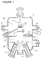
- FIG. 1 there is shown a diagrammatic sectional view of a film deposition apparatus which can be used for carrying out the process in accordance with the present invention.
- the film deposition apparatus shown basically includes a vacuum chamber 2 provided with a main evacuating apparatus 1, at least one K (Knudsen's) cell and at least one electron beam gun 11 provided at the bottom of the vacuum chamber 2, and a sample holder 5 provided at the top of the vacuum chamber 2 for holding a substrate 4 on which a film is to be deposited.
- the sample holder 5 is associated with a heater 5a for heating the substrate.
- the vacuum chamber 2 is also provided with a port 10 for exchanging a sample, a liquid nitrogen shroud 6 for forming a cold trap around an evaporation source of the K cell, and a RHEED (Reflecting High Energy Electron Diffraction) device 8 for observing the thin film roughness during the deposition.
- a shutter 9 is located for controlling a deposition time during the deposition process.
- the K cell 3 and the electron beam gun 11 are provided with an openable shutter 19.
- a gas supplying apparatus 7 is provided so as to introduce an oxidizing gas such as O 2 , O 3 , NO 2 , N 2 O, etc. in the proximity of the substrate 4 held by the sample holder 5, so that the oxidizing gas can be supplied to form an oxygen-enriched atmosphere in the proximity of the substrate 4 in order to oxidize the metal molecular beams incoming from the evaporation source in the course of the film deposition.
- an oxidizing gas such as O 2 , O 3 , NO 2 , N 2 O, etc.
- the film deposition apparatus additionally includes a partition wall 21 for dividing the vacuum chamber 2 into a first sub-chamber 2A which is constituted of a lower portion of the vacuum chamber defined below the partition wall 21 and which is coupled to the K cell 3, the electron beam gun 11 and the main evacuating apparatus 1, and a second sub-chamber 2B which is constituted of an upper portion of the vacuum chamber defined above the partition wall 21 and in which sample holder 5 is located.
- the partition wall 21 includes a through opening 23 formed at a center thereof. The position of the opening 23 is determined to ensure that a beam emitted from K cell 3 and the electron beam gun 11 toward the substrate 4 is not obstructed by the partition wall 21.
- the size of the opening 23 is determined to enable restricted molecular flows between the first sub-chamber 2A and the second sub-chamber 2B so that a pressure difference can be created between the first sub-chamber 2A and the second sub-chamber 2B when the opening 23 is open. Therefore, the partition wall 21 having the through opening 23 constitutes a vacuum impedance.
- a gate valve 22 is provided on the partition wall 21 for hermetically closing the opening 23 of the partition wall 21, so as to completely shut off the molecular flows between the first sub-chamber 2A and the second sub-chamber 2B when the gate valve 22 is closed.
- the opening and closing of this gate valve 22 is controlled from the outside of the film deposition apparatus by means which are not shown.
- an auxiliary evacuating apparatus 20 is coupled to the second sub-chamber 2B for evacuating the second sub-chamber 2B to an ultra-high vacuum when the gate valve 22 is closed.
- the auxiliary evacuating apparatus 20 is constituted of a cryopump.
- the main evacuating apparatus 1 is constituted of a diffusion pump.
- a thin film of Y 1 Ba 2 Cu 3 O 7- ⁇ oxide superconductor was prepared by using the-apparatus of Figure 1.
- an MgO (100) substrate 4 was set in the sample holder 5, and metal yttrium, metal barium and metal copper were set in three K cells 3 as evaporation sources. Thereafter, the chamber 2 was closed and the gate valve 22 was opened.
- the vacuum chamber 2 was evacuated by the main evacuating apparatus 1 and the auxiliary evacuating apparatus 20 to an ultra-high vacuum of which the pressure was lower than 1.333 x 10 -7 Pa (1 x 10 -9 Torr) in which background pressure the film deposition by the MBE process was available.
- O 2 gas including 8 volume percent O 3 was supplied from the gas supplying device 7 so that the pressure in the second chamber 2B became 6.665 x 10 -3 Pa (5 x 10 -5 Torr).
- the vacuum chamber 2 was provided with the vacuum impedance (the partition wall 21 having the through opening 23), a pressure difference of about one digit or more was created between the first sub-chamber 2A and the second sub-chamber 2B.
- the oxidizing gas jetted from the gas supplying device 7 was struck onto a deposition surface of the substrate, the pressure of the oxidizing gas on the deposition surface of the substrate was further elevated.
- the substrate 4 was heated by the heater 5a to a temperature of 700 °C.
- the K cell 3 of metal yttrium was heated to a temperature of 1220 °C
- the K cell 3 of metal barium was heated to a temperature of 620 °C
- the K cell 3 of metal copper was heated to a temperature of 1000 °C.
- the shutters 9 and 19 were opened so as to start deposition of the oxide superconductor thin film onto the substrate 4.
- a surface roughness of this deposited film was observed by the RHEED device.
- the oxide superconductor thin film was grown up to a thickness of 90 nanometers at a deposition rate of 1 nanometer/minute.
- the deposition rate is preferably 0.5 to 2 nanometers/minute.
- the substrate 4 was cooled down to the room temperature. While the substrate 4 was cooled down, it was maintained in the condition in which the oxide superconductor thin film was deposited.
- oxide superconductor thin film was obtained, crystal structure and surface condition of the oxide superconductor thin film was evaluated by LEED and XPS without exposing the oxide superconductor thin film to the air. It became clear that the oxide superconductor thin film was a c -axis orientated Y 1 Ba 2 Cu 3 O 7- ⁇ oxide superconductor thin film. The results are shown in Figures 2 to 4.
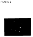
- Figure 2 shows a LEED image of the oxide superconductor thin film prepared by the above process in accordance with the present invention. In Figure 2, some spots are observed. This reveals the fact that the oxide superconductor thin film has a crystalline surface.
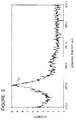
- Figures 3 and 4 show XPS spectra of the oxide superconductor thin film prepared by the above process in accordance with the present invention.
- Figure 3 shows XPS spectra in a range in which 3p peak of yttrium and a peak of C can be observed.
- no peak of C can be observed. Therefore, there is no composition of C which is a contaminant on the surface of the oxide superconductor thin film prepared by the above process in accordance with the present invention and the surface is clean.
- Figure 4 shows XPS spectra in a range in which peaks of Cu can be observed.
- intensive satellite peaks of Cu can be observed. This reveals the fact that the surface of the oxide superconductor thin film prepared by the above process in accordance with the present invention has excellent superconductivity.
- an oxide superconductor thin film which has an excellent surface condition can be obtained without any post-deposition treatment by the process in accordance with the present invention.
- the oxide superconductor thin film prepared by the process in accordance with the present invention has a high crystalline, clean and excellent superconductive surface. Therefore, the oxide superconductor thin film is suitable for a lower layer of stacked films.
Landscapes
- Chemical & Material Sciences (AREA)
- Engineering & Computer Science (AREA)
- Materials Engineering (AREA)
- Metallurgy (AREA)
- Organic Chemistry (AREA)
- Crystallography & Structural Chemistry (AREA)
- Inorganic Chemistry (AREA)
- Chemical Kinetics & Catalysis (AREA)
- Mechanical Engineering (AREA)
- Manufacturing & Machinery (AREA)
- Inorganic Compounds Of Heavy Metals (AREA)
- Superconductors And Manufacturing Methods Therefor (AREA)
Claims (11)
- Procédé de préparation d'une couche mince formée d'un supraconducteur oxyde sur un substrat par MBE, caractérisé en ce que ladite MBE est mise en oeuvre à l'aide d'un appareil de MBE comprenant une première sous-chambre (2A) dans laquelle sont placées une pluralité de sources d'évaporation et une seconde sous-chambre (2B) dans laquelle est placé ledit substrat, lesdites première et seconde sous-chambres étant séparées par une paroi de séparation (21) ayant une ouverture (23), ledit substrat étant chauffé et un gaz oxydant étant fourni localement à proximité dudit substrat de sorte que la pression de ladite seconde sous-chambre (2B) devient égale à 7,998 x 10-4 à 1,0664 x 10⁻² Pa (6 x 10⁻⁶ à 8 x 10⁻⁵ torr) tandis que la pression de ladite première sous-chambre (2A) est maintenue inférieure à 1,333 x 10-7 Pa (1 x 10⁻⁹ torr).
- Procédé selon la revendication 1, caractérisé en ce que ledit gaz oxydant est choisi dans le groupe consistant en O2 comprenant 5 à 70 % en volume de O3, N2O et NO2.
- Procédé selon la revendication 1 ou 2, caractérisé en ce que ledit substrat est refroidi jusqu'à la température ambiante après que la couche mince supraconductrice oxyde a été déposée, dans l'atmosphère dans laquelle la couche mince supraconductrice oxyde a été déposée.
- Procédé selon l'une quelconque des revendications 1 à 3, caractérisé en ce que la MBE est mise en oeuvre tandis que le gaz oxydant est projeté sur une surface de dépôt dudit substrat de manière à augmenter la pression au niveau de la surface de dépôt dudit substrat.
- Procédé selon l'une quelconque des revendications 1 à 4, caractérisé en ce que ledit supraconducteur est un supraconducteur oxyde Y1Ba2Cu3O7-δ.
- Procédé selon la revendication 5, caractérisé en ce que ladite MBE est mise en oeuvre à une température du substrat de 650 à 730°C.
- Procédé selon la revendication 6, caractérisé en ce que ladite MBE est mise en oeuvre à une température du substrat de 700°C.
- Procédé selon l'une quelconque des revendications 5 à 7, caractérisé en ce que ladite MBE est mise en oeuvre à l'aide de sources d'évaporation constituées par de l'yttrium métallique, du baryum métallique et du cuivre métallique.
- Procédé selon la revendication 8, caractérisé en ce que l'yttrium métallique, le baryum métallique et le cuivre métallique sont placés dans des cellules K.
- Procédé selon la revendication 9, caractérisé en ce que ladite MBE est mise en oeuvre à une température de la cellule K de l'yttrium métallique de 1150 à 1350°C, à une température de la cellule K du baryum métallique de 570 à 640°C et à une température de la cellule K du cuivre métallique de 950 à 1090°C.
- Procédé selon la revendication 10, caractérisé en ce que ladite MBE est mise en oeuvre à une température de la cellule K de l'yttrium métallique de 1220°C, à une température de la cellule K du baryum métallique de 620°C et à une température de la cellule K du cuivre métallique de 1000°C.
Applications Claiming Priority (2)
| Application Number | Priority Date | Filing Date | Title |
|---|---|---|---|
| JP11801592 | 1992-04-10 | ||
| JP118015/92 | 1992-04-10 |
Publications (2)
| Publication Number | Publication Date |
|---|---|
| EP0565455A1 EP0565455A1 (fr) | 1993-10-13 |
| EP0565455B1 true EP0565455B1 (fr) | 1997-12-17 |
Family
ID=14725953
Family Applications (1)
| Application Number | Title | Priority Date | Filing Date |
|---|---|---|---|
| EP93400939A Expired - Lifetime EP0565455B1 (fr) | 1992-04-10 | 1993-04-09 | Procédé de préparation d'une couche mince supraconductrice de matériau supraconducteur en oxyde composite |
Country Status (4)
| Country | Link |
|---|---|
| US (1) | US6194353B1 (fr) |
| EP (1) | EP0565455B1 (fr) |
| CA (1) | CA2093729C (fr) |
| DE (1) | DE69315736T2 (fr) |
Families Citing this family (6)
| Publication number | Priority date | Publication date | Assignee | Title |
|---|---|---|---|---|
| FR2712308B1 (fr) * | 1993-11-12 | 1996-01-26 | Lagues Michel Jean Robert | Procédé de dépôt d'un matériau sous forme de couches monomoléculaires. |
| JPH07268612A (ja) | 1994-03-29 | 1995-10-17 | Sumitomo Electric Ind Ltd | 酸化物薄膜の作製方法 |
| CA2152718A1 (fr) * | 1994-07-04 | 1996-01-05 | Takao Nakamura | Procede de fabrication de pellicules d'oxyde minces d'une grande cristallinite |
| JPH0867968A (ja) * | 1994-08-26 | 1996-03-12 | Sumitomo Electric Ind Ltd | 酸化物薄膜の作製方法 |
| GB2323209A (en) * | 1997-03-13 | 1998-09-16 | Sharp Kk | Molecular beam epitaxy apparatus and method |
| US20070032384A1 (en) * | 2005-07-26 | 2007-02-08 | The Regents Of The University Of California | Structure for improved high critical current densities in YBCO coatings |
Family Cites Families (4)
| Publication number | Priority date | Publication date | Assignee | Title |
|---|---|---|---|---|
| JPH075435B2 (ja) * | 1987-03-31 | 1995-01-25 | 住友電気工業株式会社 | 超電導薄膜の製造方法及び装置 |
| US5004721A (en) * | 1988-11-03 | 1991-04-02 | Board Of Regents, The University Of Texas System | As-deposited oxide superconductor films on silicon and aluminum oxide |
| JPH0365501A (ja) * | 1989-07-31 | 1991-03-20 | Sumitomo Electric Ind Ltd | 酸化物薄膜の作製方法 |
| CA2029038C (fr) * | 1989-10-31 | 1993-12-14 | Keizo Harada | Procede et systeme de depot d'oxyde supraconducteur en film mince |
-
1993
- 1993-04-08 CA CA002093729A patent/CA2093729C/fr not_active Expired - Fee Related
- 1993-04-09 EP EP93400939A patent/EP0565455B1/fr not_active Expired - Lifetime
- 1993-04-09 DE DE69315736T patent/DE69315736T2/de not_active Expired - Fee Related
-
1994
- 1994-10-14 US US08/323,065 patent/US6194353B1/en not_active Expired - Fee Related
Also Published As
| Publication number | Publication date |
|---|---|
| US6194353B1 (en) | 2001-02-27 |
| CA2093729C (fr) | 2001-01-02 |
| EP0565455A1 (fr) | 1993-10-13 |
| CA2093729A1 (fr) | 1993-10-11 |
| DE69315736T2 (de) | 1998-07-02 |
| DE69315736D1 (de) | 1998-01-29 |
Similar Documents
| Publication | Publication Date | Title |
|---|---|---|
| EP0655514B1 (fr) | Dispositif pour déposer des couches minces et procédé pour fabriquer des multicouches incluant des couches minces en oxyde supraconducteur | |
| EP0633331B1 (fr) | Procédé pour fabriquer un film mince d'oxyde SrTiO3 hautement cristallin | |
| US5173474A (en) | Silicon substrate having an epitaxial superconducting layer thereon and method of making same | |
| EP0698932B1 (fr) | Procédé pour fabriquer une couche mince d'oxyde à haute cristallinité et appareil pour ce procédé | |
| EP0635894B1 (fr) | Structure laminé comportant une couche mince isolante et une couche mince en supraconducteur d'oxyde | |
| US6194353B1 (en) | Process for preparing superconducting thin film formed of oxide superconductor material | |
| CA2103085C (fr) | Methode de fabrication de couches minces supraconductrices faites d'un oxyde supraconducteur a haute temperature | |
| US6172008B1 (en) | Process for preparing high crystallinity oxide thin film | |
| EP0620602B1 (fr) | Procédé de dépÔt d'un autre film mince sur un film mince en oxyde à structure cristalline perovskite | |
| US5821200A (en) | Lattice matching device and method for fabricating the same | |
| EP0691418A1 (fr) | Procédé pour fabriquer un film mince d'oxyde à haute cristallinité | |
| US5106819A (en) | Oxide superconducting tunnel junctions and manufacturing method for the same | |
| EP0505112B1 (fr) | Couche mince supraconductrice basée sur le système Bi-Sr-Ca-Cu-O et procédé pour sa production | |
| EP0637087B1 (fr) | Structure à couches comprenant une couche mince d'isolateur et une couche mince d'oxyde supraconducteur | |
| US5234901A (en) | Process for depositing a different thin film on an oxide superconductor | |
| US5314870A (en) | Preparing thin film of oxide superconductor | |
| US5236894A (en) | Process for producing a superconducting thin film at relatively low temperature | |
| US5260267A (en) | Method for forming a Bi-containing superconducting oxide film on a substrate with a buffer layer of Bi2 O3 | |
| Norton | Epitaxial growth of superconducting cuprate thin films | |
| Johnson | Secondary phase formation in YBa {sub 2} Cu {sub 3} O {sub 7-{delta}} thin films and YBa {sub 2} Cu {sub 3} O {sub 7-{delta}}/SrTiO {sub 3} superlattices | |
| Zhao et al. | Low Temperature Fabrication Of YBa2Cu3O7− x High-Tc Superconducting Thin Films By Plasma-Enhanced Metalorganic Chemical Vapor Deposition |
Legal Events
| Date | Code | Title | Description |
|---|---|---|---|
| PUAI | Public reference made under article 153(3) epc to a published international application that has entered the european phase |
Free format text: ORIGINAL CODE: 0009012 |
|
| AK | Designated contracting states |
Kind code of ref document: A1 Designated state(s): DE FR GB |
|
| 17P | Request for examination filed |
Effective date: 19931126 |
|
| 17Q | First examination report despatched |
Effective date: 19960124 |
|
| GRAG | Despatch of communication of intention to grant |
Free format text: ORIGINAL CODE: EPIDOS AGRA |
|
| GRAG | Despatch of communication of intention to grant |
Free format text: ORIGINAL CODE: EPIDOS AGRA |
|
| GRAH | Despatch of communication of intention to grant a patent |
Free format text: ORIGINAL CODE: EPIDOS IGRA |
|
| GRAH | Despatch of communication of intention to grant a patent |
Free format text: ORIGINAL CODE: EPIDOS IGRA |
|
| GRAA | (expected) grant |
Free format text: ORIGINAL CODE: 0009210 |
|
| AK | Designated contracting states |
Kind code of ref document: B1 Designated state(s): DE FR GB |
|
| REF | Corresponds to: |
Ref document number: 69315736 Country of ref document: DE Date of ref document: 19980129 |
|
| ET | Fr: translation filed | ||
| PLBE | No opposition filed within time limit |
Free format text: ORIGINAL CODE: 0009261 |
|
| STAA | Information on the status of an ep patent application or granted ep patent |
Free format text: STATUS: NO OPPOSITION FILED WITHIN TIME LIMIT |
|
| 26N | No opposition filed | ||
| REG | Reference to a national code |
Ref country code: GB Ref legal event code: IF02 |
|
| PGFP | Annual fee paid to national office [announced via postgrant information from national office to epo] |
Ref country code: GB Payment date: 20050406 Year of fee payment: 13 |
|
| PGFP | Annual fee paid to national office [announced via postgrant information from national office to epo] |
Ref country code: DE Payment date: 20050407 Year of fee payment: 13 |
|
| PGFP | Annual fee paid to national office [announced via postgrant information from national office to epo] |
Ref country code: FR Payment date: 20050408 Year of fee payment: 13 |
|
| PG25 | Lapsed in a contracting state [announced via postgrant information from national office to epo] |
Ref country code: GB Free format text: LAPSE BECAUSE OF NON-PAYMENT OF DUE FEES Effective date: 20060409 |
|
| PG25 | Lapsed in a contracting state [announced via postgrant information from national office to epo] |
Ref country code: DE Free format text: LAPSE BECAUSE OF NON-PAYMENT OF DUE FEES Effective date: 20061101 |
|
| GBPC | Gb: european patent ceased through non-payment of renewal fee |
Effective date: 20060409 |
|
| REG | Reference to a national code |
Ref country code: FR Ref legal event code: ST Effective date: 20061230 |
|
| PG25 | Lapsed in a contracting state [announced via postgrant information from national office to epo] |
Ref country code: FR Free format text: LAPSE BECAUSE OF NON-PAYMENT OF DUE FEES Effective date: 20060502 |