EP0565703B1 - Revêtement d'interférence optique à piles à film mince imbriquées - Google Patents
Revêtement d'interférence optique à piles à film mince imbriquées Download PDFInfo
- Publication number
- EP0565703B1 EP0565703B1 EP92924118A EP92924118A EP0565703B1 EP 0565703 B1 EP0565703 B1 EP 0565703B1 EP 92924118 A EP92924118 A EP 92924118A EP 92924118 A EP92924118 A EP 92924118A EP 0565703 B1 EP0565703 B1 EP 0565703B1
- Authority
- EP
- European Patent Office
- Prior art keywords
- stack
- interleaved
- stacks
- coating
- refraction
- Prior art date
- Legal status (The legal status is an assumption and is not a legal conclusion. Google has not performed a legal analysis and makes no representation as to the accuracy of the status listed.)
- Expired - Lifetime
Links
- 238000000576 coating method Methods 0.000 title claims abstract description 18
- 239000011248 coating agent Substances 0.000 title claims abstract description 16
- 230000003287 optical effect Effects 0.000 title claims abstract description 13
- 239000010409 thin film Substances 0.000 title description 5
- 239000000463 material Substances 0.000 claims abstract description 35
- 230000005855 radiation Effects 0.000 claims abstract description 7
- 230000005540 biological transmission Effects 0.000 claims description 9
- 238000000034 method Methods 0.000 description 14
- 238000002310 reflectometry Methods 0.000 description 7
- VYPSYNLAJGMNEJ-UHFFFAOYSA-N Silicium dioxide Chemical compound O=[Si]=O VYPSYNLAJGMNEJ-UHFFFAOYSA-N 0.000 description 2
- 238000012986 modification Methods 0.000 description 2
- 230000004048 modification Effects 0.000 description 2
- GWEVSGVZZGPLCZ-UHFFFAOYSA-N Titan oxide Chemical compound O=[Ti]=O GWEVSGVZZGPLCZ-UHFFFAOYSA-N 0.000 description 1
- 238000013459 approach Methods 0.000 description 1
- 238000000151 deposition Methods 0.000 description 1
- 238000002474 experimental method Methods 0.000 description 1
- 238000004519 manufacturing process Methods 0.000 description 1
- BPUBBGLMJRNUCC-UHFFFAOYSA-N oxygen(2-);tantalum(5+) Chemical compound [O-2].[O-2].[O-2].[O-2].[O-2].[Ta+5].[Ta+5] BPUBBGLMJRNUCC-UHFFFAOYSA-N 0.000 description 1
- RVTZCBVAJQQJTK-UHFFFAOYSA-N oxygen(2-);zirconium(4+) Chemical compound [O-2].[O-2].[Zr+4] RVTZCBVAJQQJTK-UHFFFAOYSA-N 0.000 description 1
- 235000012239 silicon dioxide Nutrition 0.000 description 1
- 239000000377 silicon dioxide Substances 0.000 description 1
- 230000003595 spectral effect Effects 0.000 description 1
- 238000001228 spectrum Methods 0.000 description 1
- 230000001629 suppression Effects 0.000 description 1
- 229910001936 tantalum oxide Inorganic materials 0.000 description 1
- 238000012360 testing method Methods 0.000 description 1
- OGIDPMRJRNCKJF-UHFFFAOYSA-N titanium oxide Inorganic materials [Ti]=O OGIDPMRJRNCKJF-UHFFFAOYSA-N 0.000 description 1
- 238000002834 transmittance Methods 0.000 description 1
- 229910001928 zirconium oxide Inorganic materials 0.000 description 1
Images




Classifications
-
- G—PHYSICS
- G02—OPTICS
- G02B—OPTICAL ELEMENTS, SYSTEMS OR APPARATUS
- G02B5/00—Optical elements other than lenses
- G02B5/20—Filters
- G02B5/28—Interference filters
- G02B5/281—Interference filters designed for the infrared light
- G02B5/282—Interference filters designed for the infrared light reflecting for infrared and transparent for visible light, e.g. heat reflectors, laser protection
Definitions
- the present invention describes a novel procedure for designing thin film filters using the technique of interleaving similar stacks.
- the resultant interleaved stacks can be used to make filters with extended ripple free passbands and reflectors with steep slopes.
- the 2:1 stacks are two material stacks with layers alternating between the H (high) and L (low) indices of refraction and having optical phase thicknesses such that either the H or L material is twice the optical phase thickness of the other.
- the disadvantage of this stack is, the visible passband is set by this stack and is narrow compared to the three material stacks or the interleaving technique to be described.
- the three material stacks have passbands that are wide and whose edges are not defined by one stack.
- the passband is typically described by two stacks centered at somewhat different wavelengths.
- One stack is of the three material type and centered at the longer wavelength.
- the other stack is typically a standard quarter-wave stack (i.e. alternating H and L layers with quarter-wave optical phase thicknesses) and centered at the shorter wavelength.
- the disadvantage of these stacks is, three materials with the appropriate indices of refraction must be used or one of the three indices must be synthesized from the other two.
- the novel technique of interleaving similar thin-film stacks eliminates the need to utilize stacks comprising three materials.
- the interleaving technique also achieves bandwidths in the passband similar to the three material technique.
- An optional interference coating comprising one or more interleaved stacks is known from US-A-3,737,210.
- an optical interference coating for reflecting infrared radiation and transmitting visible light comprising: one or more interleaved stacks said interleaved stacks comprising a first stack containing three alternating layers of high and low refractive index materials of form (L/a bH L/a), and a second stack containing three alternating layers of high and low refractive index materials of the form (H/a bL H/a); wherein L and H are a low and a high index of refraction material respectively, L and H each being defined as having an optical thickness of a multiple of a quarter-wave of the stack wavelength; and wherein a and b are predetermined values in the ranges of: 1.75 ⁇ a ⁇ 2.5 and 2.75 ⁇ b ⁇ 3.25.
- the present invention describes an interference coating for reflecting infrared radiation and transmitting visible light.
- the coating is formed from one or more interleaved stacks and a third standard quarter wave stack.
- An interleaved stack is made from two similar stacks.
- the first stack is made of three layers of the form (L/a bH L/a).
- the second stack is made of three layers of the form (H/a bL H/a).
- the interleaved stack is a plurality of a combined first and second stack and is of the form [(L/a bH L/a) (H/a bL H/a)].
- L and H refer to materials of low and high indices of refraction respectively
- a and b refer to the thickness of each layer.
- Herpin equivalent stack in its simplest form can be described with the notation (pgp).
- p and q are typically two materials of H-high and L-low indices of refraction.
- the arrangement of the H and L materials are such that the outer layers, the layers designated by p, have the same index of refraction and the same optical and physical thicknesses. This arrangement makes it simple to calculate what is known as the effective index and optical phase thickness at a particular wavelength.
- the interleaving technique uses this information to predict the regions of high reflectivity and high transmission.
- a standard thin film filter is typically made by depositing multiple Herpin equivalent stacks.
- the notation for this type of stack arrangement is (pqp) n . Where n is the number of times the stack is repeated.
- n is the number of times the stack is repeated.
- the two stacks (L/2 H L/2) and (H/2 L H/2) are both of the form (pqp).
- the only difference is that the H and L have been swapped. Spectrally their performance is similar. The location of the high reflection and transmission regions are the same. The only difference is the amplitude of the ripple in the transmission regions.
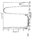
- Figs. 1 and 2. Fig. 1 shows a stack of the form (L/2 H L/2) 8 and Fig. 2 shows a stack of the form (H/2 L H/2) 8 .
- the value for L was 1.44 and the value for H was 2.0.
- an (L/2 H L/2) will be added to the complete interleaved stack.
- This interleaved arrangement will yield a high reflection region whenever two properties are satisfied.
- the second property requires that the ratio of the Herpin equivalent indices of the two (pqp) stacks of the basic stack be greater or less than one. The further the ratio is from unity the higher the reflection.
- the second property is the one that contributes to extending the high transmission regions and increasing the slopes at the edges of the high reflection regions.
- the high reflection regions will occur at wavelengths 3000nm, 1000nm, 600nm, 428nm, 333nm, 272, 230 and 200nm with minor peaks at 3000nm, 428nm, 333nm and 200nm. All the major peaks have effective indice ratios of 2.983/1.062 or 2.81 and all minor peaks have effective indice ratios of 1.623/1.952 or .831.
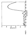
- Figs. 3 and 4 are graphs of the wavelength versus reflectance for an interleaved stack made from the Herpin equivalents shown in Tables 1 and 2. As can be seen the interleaving technique allows the suppression of reflection peaks whenever property one is satisfied and property two has a ratio that approaches unity.
- the thickness of the q layer in the (pqp) stack needs to be increased.
- the basic stack has the form ((L/2 3H L/2) (H/2 3L H/2)) n and the center wavelength of the stack is 425nm a major peak will occur near 1700 nm and 340nm with a minor peak near 566nm. Since the ratio of the effective indices at the minor peak is approximately .91 this peak is effectively suppressed. Therefore, the interleaving technique has achieved a bandwidth for the high transmission region greater than 1000 nm. If two interleaved stacks of this form are used along with a standard Herpin stack an IR reflective stack with the performance described above can be achieved.
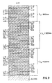
- the complete stack configuration is:
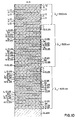
- This stack has some ripple in the passband that needs to be suppressed. This is done in two ways. First matching layers are placed on either side of the interleaved stacks. Matching layers are of the form LL H/2.25 and H/2.25 and are shown in the arrangement below. The matching layers shown are not in parenthesis. Second the minor peak associated with the interleaved stacks is further suppressed by simply making the eighth wave layers, those designated by L/2 and H/2, slightly thinner. The final stack arrangement, also shown in Fig. 10, is:
- the indices of the materials used to manufacture this coating should be about 1.40-1.50 for the low index material and 2.0-2.2 for the high index material.
- Silicon dioxide would be the logical choice for the low index material and a material such as titanium oxide, tantalum oxide, or zirconium oxide for the high index material. It is not the absolute value of the index of refraction of the high or low material but the ratio between the high index material and the low index material.
- Fig. 7 shows a comparison of the reflectance of interleaved stacks of the present invention with prior art stacks (2:1) published in UK Patent Application 2103830A.
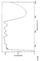
- Fig. 7 shows that the interleaved stacks allows transmittance of light over a greater wavelength window ( ⁇ 400nm to 800nm) than in the 2:1 stack.
- Fig. 8 shows a comparison of the reflectance of the interleaved stacks of the present invention with prior art stacks (3 material) published in European Patent Application 90307792.3. Fig. 8 shows that the interleaved stacks perform comparably to the 3 material stacks.
Landscapes
- Physics & Mathematics (AREA)
- General Physics & Mathematics (AREA)
- Optics & Photonics (AREA)
- Optical Filters (AREA)
Abstract
Claims (4)
- Revêtement d'interférence optique pour réfléchir un rayonnement infrarouge et transmettre la lumière visible, comprenant:un ou plusieurs empilement(s) imbriqué(s), les dits empilements imbriqués comprenant un premier empilement contenant trois couches alternées de matériaux à indices de réfraction bas et élevé de forme (L/a bH L/a), et un deuxième empilement contenant trois couches alternées de matériaux à indices de réfraction élevé et bas (H/a bL H/a);dans lequel L et H sont respectivement des matériaux d'indices bas et élevé, L et H étant chacun définis comme ayant une épaisseur optique d'un multiple du quart d'onde de la longueur d'onde de l'empilement ; etdans lequel a et b sont des valeurs prédéterminées dans les gammes suivantes :


- Revêtement selon la revendication 1, comprenant, en outre, un empilement de la forme (L/a bH L/a) ajouté à un côté d'un ou de plusieurs empilement(s) imbriqué(s) pour obtenir une symétrie.
- Revêtement selon la revendication 1 ou 2, comprenant, en outre, un ou plusieurs empilement(s) de la forme (L/2 H L/2) ajouté(s) à un ou plusieurs empilement(s) imbriqué(s) pour définir la largeur de la bande de transmission pour un réflecteur d'un rayonnement infrarouge.
- Revêtement selon la revendication 1, 2 ou 3, dans lequel l'indice de réfraction bas du matériau a une valeur comprise approximativement entre 1,40 et 1,50 et l'indice de réfraction élevé du matériau a une valeur comprise approximativement entre 2,0 et 2,2.
Applications Claiming Priority (3)
| Application Number | Priority Date | Filing Date | Title |
|---|---|---|---|
| US07/787,855 US5179468A (en) | 1991-11-05 | 1991-11-05 | Interleaving of similar thin-film stacks for producing optical interference coatings |
| US787855 | 1991-11-05 | ||
| PCT/US1992/009050 WO1993009449A1 (fr) | 1991-11-05 | 1992-10-26 | Revetement d'interference optique a piles a film mince imbriquees |
Publications (2)
| Publication Number | Publication Date |
|---|---|
| EP0565703A1 EP0565703A1 (fr) | 1993-10-20 |
| EP0565703B1 true EP0565703B1 (fr) | 1997-07-09 |
Family
ID=25142716
Family Applications (1)
| Application Number | Title | Priority Date | Filing Date |
|---|---|---|---|
| EP92924118A Expired - Lifetime EP0565703B1 (fr) | 1991-11-05 | 1992-10-26 | Revêtement d'interférence optique à piles à film mince imbriquées |
Country Status (5)
| Country | Link |
|---|---|
| US (1) | US5179468A (fr) |
| EP (1) | EP0565703B1 (fr) |
| CA (1) | CA2097811A1 (fr) |
| DE (1) | DE69220775T2 (fr) |
| WO (1) | WO1993009449A1 (fr) |
Families Citing this family (52)
| Publication number | Priority date | Publication date | Assignee | Title |
|---|---|---|---|---|
| GB2261523B (en) * | 1985-11-01 | 1993-12-08 | Barr & Stroud Ltd | Optical filters |
| DE4221523A1 (de) * | 1992-07-01 | 1994-01-05 | Jenoptik Jena Gmbh | Strahlenschutzanordnung mit integriertem Bestrahlungs-Indikator |
| US5410431A (en) * | 1993-06-01 | 1995-04-25 | Rockwell International Corporation | Multi-line narrowband-pass filters |
| US5563729A (en) * | 1993-08-30 | 1996-10-08 | Minolta Co., Ltd. | Image forming light scanning apparatus |
| EP0657752A1 (fr) * | 1993-12-08 | 1995-06-14 | Osram Sylvania Inc. | Couche optique et lampe munie de celle-ci |
| DE4401270A1 (de) * | 1994-01-18 | 1995-07-20 | Patent Treuhand Ges Fuer Elektrische Gluehlampen Mbh | Reflektorlampe |
| US5646781A (en) * | 1995-05-15 | 1997-07-08 | Omega Optical, Inc. | Optical filters for forming enhanced images |
| US5705882A (en) * | 1995-10-20 | 1998-01-06 | Osram Sylvania Inc. | Optical coating and lamp employing same |
| US5751466A (en) * | 1996-01-11 | 1998-05-12 | University Of Alabama At Huntsville | Photonic bandgap apparatus and method for delaying photonic signals |
| US5777793A (en) * | 1996-07-25 | 1998-07-07 | Northern Telecom Limited | Polarization insensitive multilayer planar reflection filters with near ideal spectral response |
| US6262830B1 (en) | 1997-09-16 | 2001-07-17 | Michael Scalora | Transparent metallo-dielectric photonic band gap structure |
| US5907427A (en) | 1997-10-24 | 1999-05-25 | Time Domain Corporation | Photonic band gap device and method using a periodicity defect region to increase photonic signal delay |
| US6967778B1 (en) | 1998-01-13 | 2005-11-22 | 3M Innovative Properties Co. | Optical film with sharpened bandedge |
| US6157490A (en) * | 1998-01-13 | 2000-12-05 | 3M Innovative Properties Company | Optical film with sharpened bandedge |
| US6049419A (en) | 1998-01-13 | 2000-04-11 | 3M Innovative Properties Co | Multilayer infrared reflecting optical body |
| US6028693A (en) * | 1998-01-14 | 2000-02-22 | University Of Alabama In Huntsville | Microresonator and associated method for producing and controlling photonic signals with a photonic bandgap delay apparatus |
| US6744552B2 (en) * | 1998-04-02 | 2004-06-01 | Michael Scalora | Photonic signal frequency up and down-conversion using a photonic band gap structure |
| US6304366B1 (en) | 1998-04-02 | 2001-10-16 | Michael Scalora | Photonic signal frequency conversion using a photonic band gap structure |
| US6396617B1 (en) | 1999-05-17 | 2002-05-28 | Michael Scalora | Photonic band gap device and method using a periodicity defect region doped with a gain medium to increase photonic signal delay |
| US6538794B1 (en) | 1999-09-30 | 2003-03-25 | D'aguanno Giuseppe | Efficient non-linear phase shifting using a photonic band gap structure |
| FR2801684B1 (fr) * | 1999-11-26 | 2002-04-26 | Commissariat Energie Atomique | Filtre anticalorique et procede de fabrication de ce filtre |
| US6414780B1 (en) | 1999-12-23 | 2002-07-02 | D'aguanno Giuseppe | Photonic signal reflectivity and transmissivity control using a photonic band gap structure |
| US6339493B1 (en) | 1999-12-23 | 2002-01-15 | Michael Scalora | Apparatus and method for controlling optics propagation based on a transparent metal stack |
| CN1278378C (zh) * | 2000-06-16 | 2006-10-04 | 皇家菲利浦电子有限公司 | 包括光吸收介质的电灯 |
| JP2003015175A (ja) | 2001-04-27 | 2003-01-15 | Mitsubishi Electric Corp | 固体光源装置 |
| US6611378B1 (en) | 2001-12-20 | 2003-08-26 | Semrock, Inc. | Thin-film interference filter with quarter-wavelength unit sub-layers arranged in a generalized pattern |
| US7453190B2 (en) * | 2002-02-22 | 2008-11-18 | Koninklijke Philips Electronics | Electric lamp with absorbing and interference media |
| US7927703B2 (en) * | 2003-04-11 | 2011-04-19 | 3M Innovative Properties Company | Adhesive blends, articles, and methods |
| EP1635860A2 (fr) * | 2003-06-12 | 2006-03-22 | Ludwig Institute For Cancer Research | Utilisation de vegf-c ou de vegf-d en chirurgie reconstructive |
| DE10354091B4 (de) * | 2003-09-29 | 2007-02-01 | Fraunhofer-Gesellschaft zur Förderung der angewandten Forschung e.V. | Optisches System zur Verringerung der Reflexion optischer transparenter Substrate |
| EP1751586A2 (fr) * | 2003-09-29 | 2007-02-14 | Fraunhofer-Gesellschaft zur Förderung der angewandten Forschung e.V. | Systeme optique pour reduire la reflexion de substrats optiques transparents |
| US7352118B2 (en) | 2003-12-10 | 2008-04-01 | General Electric Company | Optimized ultraviolet reflecting multi-layer coating for energy efficient lamps |
| US7133197B2 (en) * | 2004-02-23 | 2006-11-07 | Jds Uniphase Corporation | Metal-dielectric coating for image sensor lids |
| DE102004021494B4 (de) * | 2004-04-30 | 2006-04-06 | Man Roland Druckmaschinen Ag | Vorrichtung zum Auf- und Abziehen einer Hülse |
| ATE377580T1 (de) | 2004-07-12 | 2007-11-15 | Cardinal Cg Co | Wartungsarme beschichtungen |
| CN1828345A (zh) * | 2005-03-04 | 2006-09-06 | 鸿富锦精密工业(深圳)有限公司 | 一种滤光装置及其制造方法 |
| US7162141B1 (en) * | 2005-10-18 | 2007-01-09 | Jds Unipahse Corporation | Electro-conductive anti-reflection coating |
| CN100386655C (zh) * | 2005-10-27 | 2008-05-07 | 亚洲光学股份有限公司 | 三通道滤光片 |
| CN100430757C (zh) * | 2005-12-08 | 2008-11-05 | 亚洲光学股份有限公司 | 可减少镀膜层数的带通滤光片 |
| WO2007111985A2 (fr) * | 2006-03-24 | 2007-10-04 | Goodrich Corporation | Réseau de diffraction optique et procédé de fabrication |
| WO2007121215A1 (fr) | 2006-04-11 | 2007-10-25 | Cardinal Cg Company | Revêtements photocatalytiques dotés de propriétés améliorées permettant un entretien minime |
| US20080011599A1 (en) | 2006-07-12 | 2008-01-17 | Brabender Dennis M | Sputtering apparatus including novel target mounting and/or control |
| CA2664369A1 (fr) * | 2007-09-14 | 2009-03-19 | Cardinal Cg Company | Revetements a faible entretien et procedes de production de revetements a faible entretien |
| US20100270479A1 (en) * | 2007-11-12 | 2010-10-28 | Cornell University | Non-imaging, weakly focused fluorescence emission apparatus and method |
| CN101909509B (zh) * | 2007-11-12 | 2013-03-27 | 康奈尔大学 | 多路径、多放大率、非共焦荧光发射内窥镜装置和方法 |
| DE102008016457A1 (de) * | 2008-03-31 | 2009-10-01 | Osram Gesellschaft mit beschränkter Haftung | Leuchtvorrichtung |
| EP2246630B1 (fr) | 2009-04-30 | 2017-11-29 | Electrolux Home Products Corporation N.V. | Four, plus particulièrement un four ménager |
| US8098969B2 (en) * | 2009-12-08 | 2012-01-17 | Onechip Photonics Inc. | Waveguide optically pre-amplified detector with passband wavelength filtering |
| JP6264798B2 (ja) * | 2013-09-13 | 2018-01-24 | 日油株式会社 | 転写用波長選択的反射フィルム並びにそれを用いた転写方法及び転写成型物 |
| JP2017009703A (ja) * | 2015-06-18 | 2017-01-12 | キヤノン株式会社 | 多層膜を用いた光学素子および光学機器 |
| US10604442B2 (en) | 2016-11-17 | 2020-03-31 | Cardinal Cg Company | Static-dissipative coating technology |
| JP7143881B2 (ja) * | 2018-03-26 | 2022-09-29 | Jsr株式会社 | 光学フィルターおよびその用途 |
Family Cites Families (7)
| Publication number | Priority date | Publication date | Assignee | Title |
|---|---|---|---|---|
| GB1244002A (en) * | 1968-10-23 | 1971-08-25 | Howard Grubb Parsons & Company | Improvements in and relating to interference filters |
| US3737210A (en) * | 1972-03-31 | 1973-06-05 | Bausch & Lomb | Multilayer filter based on substitution of herpin equivalent layers in a antireflection coating formula |
| CH556548A (de) * | 1972-09-19 | 1974-11-29 | Balzers Patent Beteilig Ag | Aus abwechselnd hoch- und niederbrechenden oxidschichten aufgebautes verlustarmes, hochreflektierendes vielschichtsystem. |
| CA1177704A (fr) * | 1981-07-20 | 1984-11-13 | James D. Rancourt | Enduits optiques pour emploi a temperatures elevees |
| US4854670A (en) * | 1986-12-17 | 1989-08-08 | Gte Products Corporation | Wide angle optical filters |
| US4931315A (en) * | 1986-12-17 | 1990-06-05 | Gte Products Corporation | Wide angle optical filters |
| CA2017471C (fr) * | 1989-07-19 | 2000-10-24 | Matthew Eric Krisl | Revetements de filtrage optique et lampes utilisant ces revetements |
-
1991
- 1991-11-05 US US07/787,855 patent/US5179468A/en not_active Expired - Lifetime
-
1992
- 1992-10-26 EP EP92924118A patent/EP0565703B1/fr not_active Expired - Lifetime
- 1992-10-26 DE DE69220775T patent/DE69220775T2/de not_active Expired - Fee Related
- 1992-10-26 WO PCT/US1992/009050 patent/WO1993009449A1/fr not_active Ceased
- 1992-10-26 CA CA002097811A patent/CA2097811A1/fr not_active Abandoned
Also Published As
| Publication number | Publication date |
|---|---|
| DE69220775T2 (de) | 1998-02-12 |
| CA2097811A1 (fr) | 1993-05-06 |
| DE69220775D1 (de) | 1997-08-14 |
| WO1993009449A1 (fr) | 1993-05-13 |
| EP0565703A1 (fr) | 1993-10-20 |
| US5179468A (en) | 1993-01-12 |
Similar Documents
| Publication | Publication Date | Title |
|---|---|---|
| US5179468A (en) | Interleaving of similar thin-film stacks for producing optical interference coatings | |
| US4793669A (en) | Multilayer optical filter for producing colored reflected light and neutral transmission | |
| US4896928A (en) | Chromatically invariant multilayer dielectric thin film coating | |
| US5926317A (en) | Multilayer thin film dielectric bandpass filter | |
| USRE33729E (en) | Multilayer optical filter for producing colored reflected light and neutral transmission | |
| US4756602A (en) | Narrowband optical filter with partitioned cavity | |
| US4179181A (en) | Infrared reflecting articles | |
| US4960310A (en) | Broad band nonreflective neutral density filter | |
| US5400174A (en) | Optical notch or minus filter | |
| US7006292B2 (en) | Multi-cavity optical filter | |
| US5719989A (en) | Multilayer thin film bandpass filter | |
| US6231992B1 (en) | Partial reflector | |
| US5999322A (en) | Multilayer thin film bandpass filter | |
| CN1979230B (zh) | 介质多层滤光器 | |
| US5410431A (en) | Multi-line narrowband-pass filters | |
| US6018421A (en) | Multilayer thin film bandpass filter | |
| JP3041094B2 (ja) | ピーク抑制を有する光学的に可変な干渉装置及び方法 | |
| US4826267A (en) | Spectral filter with integral antireflection coating | |
| US3737210A (en) | Multilayer filter based on substitution of herpin equivalent layers in a antireflection coating formula | |
| CA2122929C (fr) | Filtre large bande type "rugate" | |
| KR0124493B1 (ko) | 공간적으로 파장이 변하는 루게이트 광학 필터 및 그 운용 방법 | |
| GB2070275A (en) | Interference mirrors | |
| JP2008032804A (ja) | 光学素子 | |
| TWI800421B (zh) | 可擴充帶寬的組合式帶通濾光片組 | |
| Nenkov et al. | Broad-band heat reflector design using five-layer symmetrical periods from non-absorbing high-and low-refractive-index materials |
Legal Events
| Date | Code | Title | Description |
|---|---|---|---|
| PUAI | Public reference made under article 153(3) epc to a published international application that has entered the european phase |
Free format text: ORIGINAL CODE: 0009012 |
|
| 17P | Request for examination filed |
Effective date: 19930802 |
|
| AK | Designated contracting states |
Kind code of ref document: A1 Designated state(s): BE DE FR GB NL |
|
| 17Q | First examination report despatched |
Effective date: 19950505 |
|
| GRAG | Despatch of communication of intention to grant |
Free format text: ORIGINAL CODE: EPIDOS AGRA |
|
| GRAH | Despatch of communication of intention to grant a patent |
Free format text: ORIGINAL CODE: EPIDOS IGRA |
|
| GRAH | Despatch of communication of intention to grant a patent |
Free format text: ORIGINAL CODE: EPIDOS IGRA |
|
| GRAA | (expected) grant |
Free format text: ORIGINAL CODE: 0009210 |
|
| AK | Designated contracting states |
Kind code of ref document: B1 Designated state(s): BE DE FR GB NL |
|
| REF | Corresponds to: |
Ref document number: 69220775 Country of ref document: DE Date of ref document: 19970814 |
|
| ET | Fr: translation filed | ||
| PLBE | No opposition filed within time limit |
Free format text: ORIGINAL CODE: 0009261 |
|
| STAA | Information on the status of an ep patent application or granted ep patent |
Free format text: STATUS: NO OPPOSITION FILED WITHIN TIME LIMIT |
|
| 26N | No opposition filed | ||
| REG | Reference to a national code |
Ref country code: GB Ref legal event code: 732E |
|
| REG | Reference to a national code |
Ref country code: GB Ref legal event code: IF02 |
|
| PGFP | Annual fee paid to national office [announced via postgrant information from national office to epo] |
Ref country code: GB Payment date: 20031023 Year of fee payment: 12 |
|
| PGFP | Annual fee paid to national office [announced via postgrant information from national office to epo] |
Ref country code: FR Payment date: 20031026 Year of fee payment: 12 |
|
| PGFP | Annual fee paid to national office [announced via postgrant information from national office to epo] |
Ref country code: BE Payment date: 20031030 Year of fee payment: 12 |
|
| PGFP | Annual fee paid to national office [announced via postgrant information from national office to epo] |
Ref country code: NL Payment date: 20031031 Year of fee payment: 12 |
|
| PGFP | Annual fee paid to national office [announced via postgrant information from national office to epo] |
Ref country code: DE Payment date: 20031230 Year of fee payment: 12 |
|
| PG25 | Lapsed in a contracting state [announced via postgrant information from national office to epo] |
Ref country code: GB Free format text: LAPSE BECAUSE OF NON-PAYMENT OF DUE FEES Effective date: 20041026 |
|
| PG25 | Lapsed in a contracting state [announced via postgrant information from national office to epo] |
Ref country code: BE Free format text: LAPSE BECAUSE OF NON-PAYMENT OF DUE FEES Effective date: 20041031 |
|
| BERE | Be: lapsed |
Owner name: *OSRAM SYLVANIA INC. Effective date: 20041031 |
|
| PG25 | Lapsed in a contracting state [announced via postgrant information from national office to epo] |
Ref country code: NL Free format text: LAPSE BECAUSE OF NON-PAYMENT OF DUE FEES Effective date: 20050501 |
|
| PG25 | Lapsed in a contracting state [announced via postgrant information from national office to epo] |
Ref country code: DE Free format text: LAPSE BECAUSE OF NON-PAYMENT OF DUE FEES Effective date: 20050503 |
|
| GBPC | Gb: european patent ceased through non-payment of renewal fee |
Effective date: 20041026 |
|
| PG25 | Lapsed in a contracting state [announced via postgrant information from national office to epo] |
Ref country code: FR Free format text: LAPSE BECAUSE OF NON-PAYMENT OF DUE FEES Effective date: 20050630 |
|
| NLV4 | Nl: lapsed or anulled due to non-payment of the annual fee |
Effective date: 20050501 |
|
| REG | Reference to a national code |
Ref country code: FR Ref legal event code: ST |
|
| BERE | Be: lapsed |
Owner name: *OSRAM SYLVANIA INC. Effective date: 20041031 |