EP0566963A2 - Apparat zur Produktion eines Musterbildes - Google Patents
Apparat zur Produktion eines Musterbildes Download PDFInfo
- Publication number
- EP0566963A2 EP0566963A2 EP93105982A EP93105982A EP0566963A2 EP 0566963 A2 EP0566963 A2 EP 0566963A2 EP 93105982 A EP93105982 A EP 93105982A EP 93105982 A EP93105982 A EP 93105982A EP 0566963 A2 EP0566963 A2 EP 0566963A2
- Authority
- EP
- European Patent Office
- Prior art keywords
- specimen
- focusing
- dimensional
- dimensional image
- electron beam
- Prior art date
- Legal status (The legal status is an assumption and is not a legal conclusion. Google has not performed a legal analysis and makes no representation as to the accuracy of the status listed.)
- Withdrawn
Links
Images


Classifications
-
- H—ELECTRICITY
- H01—ELECTRIC ELEMENTS
- H01J—ELECTRIC DISCHARGE TUBES OR DISCHARGE LAMPS
- H01J37/00—Discharge tubes with provision for introducing objects or material to be exposed to the discharge, e.g. for the purpose of examination or processing thereof
- H01J37/26—Electron or ion microscopes; Electron or ion diffraction tubes
- H01J37/28—Electron or ion microscopes; Electron or ion diffraction tubes with scanning beams
-
- G—PHYSICS
- G01—MEASURING; TESTING
- G01B—MEASURING LENGTH, THICKNESS OR SIMILAR LINEAR DIMENSIONS; MEASURING ANGLES; MEASURING AREAS; MEASURING IRREGULARITIES OF SURFACES OR CONTOURS
- G01B15/00—Measuring arrangements characterised by the use of electromagnetic waves or particle radiation, e.g. by the use of microwaves, X-rays, gamma rays or electrons
-
- H—ELECTRICITY
- H01—ELECTRIC ELEMENTS
- H01J—ELECTRIC DISCHARGE TUBES OR DISCHARGE LAMPS
- H01J2237/00—Discharge tubes exposing object to beam, e.g. for analysis treatment, etching, imaging
- H01J2237/22—Treatment of data
- H01J2237/226—Image reconstruction
-
- H—ELECTRICITY
- H01—ELECTRIC ELEMENTS
- H01J—ELECTRIC DISCHARGE TUBES OR DISCHARGE LAMPS
- H01J2237/00—Discharge tubes exposing object to beam, e.g. for analysis treatment, etching, imaging
- H01J2237/26—Electron or ion microscopes
- H01J2237/28—Scanning microscopes
- H01J2237/2809—Scanning microscopes characterised by the imaging problems involved
- H01J2237/281—Bottom of trenches or holes
Definitions
- the present invention relates to a specimen image producing apparatus, and more particularly to a specimen image producing apparatus for producing an image of a specimen by scanning the same with a charged-particle beam.
- an electron beam is focused on a specimen by a focusing lens system, the specimen is scanned with the focused electron beam so as to generate an information signal characteristic of the specimen such as secondary electron signal and backscattered electron signal therefrom, and the generated information signal is used to produce an image of the specimen to be displayed on a display.
- the most typical method for observing the surface outline of the specimen in three dimensions is to photograph two images of the specimen obtained when the incident angle of the electron beam on the specimen is selectively set to - ⁇ and + ⁇ .
- the incident angle of the electron beam on the specimen may be set by tilting the specimen relative to the electron beam.
- the setting of the incident angle may also be made by tilting the electron beam relative to the sample as disclosed in Japanese patent application laid-open No. 61-19044(1986).
- it is possible to quantitatively measure three-dimensionally the surface structure of the specimen by analyzing the photographed images as disclosed in Japanese patent application laid-open No. 62-96807(1987).
- a sample or specimen is scanned with a focused ion beam to thereby generate secondary ions or secondary electrons from the specimen, and the generated secondary information may be used not only for conducting the analysis of the specimen in the direction of deepness thereof but also for producing an image of the specimen.
- the above mentioned problems in connection with the scanning electron microscope are also applicable to the ion microanalyzer.
- An object of the present invention is to provide a specimen image producing apparatus adapted to three -dimensionally observe the surface of a specimen.
- Another object of the present invention is to provide a specimen image producing apparatus adapted to three-dimensionally observe that portion of interest on the surface of a specimen which is composed of a protrusion and/or recess, even if the height or deepness of the portion is greater than the depth of focus of a focusing lens system for focusing a charged-particle beam on the specimen.
- An additional object of the present invention is to provide a specimen image producing apparatus adapted to three-dimensionally observe the surface of a specimen without tilting one of the specimen and a charged-particle beam directed to the specimen relative to the other thereof.
- a yet another object of the present invention is to provide a specimen image producing apparatus adapted to measure the height or deepness of that portion of interest on the surface of a specimen which is composed of a protrusion and/or recess.
- a further object of the present invention is to provide a specimen image producing apparatus adapted to three-dimensionally observe and measure a portion of interest on the surface of a specimen.
- a specimen image producing apparatus which comprises means for generating a charged-particle beam, means for focusing the charged-particle beam on a specimen, means for scanning the specimen with the focused charged-particle beam in two dimensions under a plurality of focusing conditions so as to generate corresponding two-dimensional image signals from the specimen, respectively, and means for producing a three -dimensional information image on the basis of the plurality of focusing conditions and the corresponding two-dimensional image signals.
- FIG.1 there is shown an embodiment of a scanning electron microscope according to the present invention.
- An extraction voltage Ve is applied between a field emission tip 1 and an extraction electrode 2, whereby electrons are field-emitted from the field emission tip 1, are passed through an opening of the extraction electrode 2 in the form of an electron beam and then are accelerated by an accelerating voltage Va applied between the field emission tip 1 and a grounded accelerating electrode 3 to thereby to be passed through an opening thereof.
- the electron beam is focused on a specimen 4 by a focusing lens system which comprises a condenser lens 5 and an objective lens 6. Further, the focused electron beam is two-dimensionally deflected by a electron beam deflector 7 so that the specimen is two-dimensionally scanned with the focused electron beam, whereby secondary electrons, backscattered electrons, X-rays, and so on characteristic of the specimen 4 are generated therefrom.
- the secondary electrons are detected and converted into an electric signal by a detector 8.
- the electric signal is converted into a digital signal by an analog-to-digital converter 9 and then is stored in the form of a two-dimensional image signal, i. e. picture image signal in a frame memory included in a memory unit 10.
- the digital signal for the condenser lens 5 is read out from the memory unit 10 and is converted by the digital-to-analog converter 11 into an analog signal which drives a supply source 12 so as to energize the condenser lens 5.
- the digital signals for the objective lens 6 and the electron beam deflector 7 are read out from the memory unit 10, respectively, and are converted by digital-to-analog converters 13 and 14 into analog signals which drive the supply sources 15 and 16 so as to energize the objective lens 6 and the electron beam deflector 7, respectively.
- a microprocessor 17 in addition to the performing of various operations, is so operated as to not only vary the excitation current flowing through the objective lens 6 for changing the focusing position of the electron beam relative to the specimen 4 and the scanning signal applied to the electron beam deflector 7 for changing the observing magnification of the specimen but also display on an output unit 18 two markers and displace these separately from each other, in response to instructions from an input unit 19 which includes manipulators such as controls, buttons and keys.
- the detector 8 if a protrusion 4a on the surface of the specimen 4 is scanned with the electron beam as shown in Fig.2(a), the detector 8 outputs a signal to be stored in the frame memory which greatly changes within the depth of focus and does not substantially change out of the depth of focus because the electron beam is widen, as shown in Fig.2(b). If the outputted signal stored in the frame memory is subject to a differentiation processing, a waveform as shown in Fig.2(c) is obtained, and further, if upper and lower levels are set so that the differentiated signal within the depth of focus is out of the range smaller than the upper level and larger than the lower level, positions X1 and X2 are detectable distinguishably from other positions.
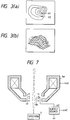
- Two-dimensional position information images, i. e. cross-section contour images are obtained in the same manner as above by changing the focusing position of the electron beam relative to the specimen, and further, a plurality of thus produced cross-section contour images are superposed on each other, whereby a three-dimensional information image of the specimen may be displayed in a contour map as shown in Fig.3(a).
- a three-dimensional information image may be displayed in a birds-eye view represented by a wire frame such as illustrated in Fig. 3(b).
- an initial or start focusing position of the electron beam relative to the specimen 4 is set as a standard or reference focusing position (Step 20).
- This reference focusing position may be set by the operator taking into account the height or deepness of protrusions and/or recesses on the surface of the specimen 4 in connection with the depth of focus of the objective lens 6.
- the specimen 4 is two-dimensionally scanned with the electron beam under the focusing position condition set as above and under a given magnification condition (Step 21), an image signal generated thereby from the specimen being stored in the memory unit 10 as a two-dimensional image signal, i. e. picture image signal together with the focusing position condition under which the two-dimensional image signal has been obtained (Step 22).
- step 23 when the storage of all the image signals have not yet been completed, the following steps are continued. That is, a variation ⁇ Z in the focusing position necessary for producing a three-dimensional information image of the specimen is set (Step 24). Then, a variation ⁇ I in the excitation current of the objective lens 6 which causes the focusing position of the electron beam to change by ⁇ Z is set (Step 25). This may be calculated from ⁇ Z on the basis of a given relationship between the excitation current of the objective lens 6 and the focusing position of the electron beam relative to the specimen 4, or read out from a memory table prepared in advance which is representative of the relationship of ⁇ I values to ⁇ Z values corresponding thereto. Finally, after changing the excitation current of the objective lens 6 (Step 26), the flow chart step returns to the step 21 to repeat the steps 21 to 26.
- step 23 when the storage of all the two -dimensional image signals is judged to have been completed, the step advances to the following three-dimensional information image generation and display processing.
- Step 27 extraction is made of positions at which the two-dimensional image signal within the depth of focus is obtained, and the extracted positions are linked to each other to thereby form a two-dimensional position information image (Step 27).
- the followings may be used in order to discriminate positions where the image signal within the depth of focus is obtained from other positions.
- Such two-dimensional position information images as above further being represented by binary system in a line drawing and being stored in the memory unit 10 per corresponding focusing condition, i. e. focusing position of the electron beam relative to the specimen, they can be fetched to generate a set of three-dimensional coordinates expressing the outline of the surface of the specimen.
- any desired three-dimensional information image corresponding to a specific object can be generated and displayed in the manners as follows.
- each position at each point thereof in the travelling direction of the electron beam being definite, thereby it is possible to render each position in differentiated brightness or colors in response to each position in the travelling direction of the electron beam, thus capable of displaying a three-dimensional information image in a form easier to recognize on the display.
- Fig.5 shows a flow chart of one embodiment for conducting a three-dimensional measurement according to the present invention.
- This embodiment illustrates an example of the three-dimensional measurement to be conducted utilizing the contour map display (Step 28) explained in Fig.4. Therefore, until the contour map displaying at 28, the same steps as in the flow chart of Fig.4 are carried out, thereat displaying the image of Fig.3(a). Step 28 is indicated as step 30 in Fig.5.
- Two markers are displayed in superposition on the contour map as (Step 31) and points (H1,H2) desired to be measured are designated with the two markers shown in Fig.3(a) (Step 32).
- position signals (Z1,Z2) corresponding to these two points (H1,H2) are read out from the memory unit 10 (Step 33). Because these position signals (Z1,Z2) indicate a height of each point (H1,H2), a difference ⁇ Z obtained between the position signals of these two points (Step 34) can be measured as a height between these designated two points (H1,H2).
- the focusing position of the electron beam is utilized as the position signals (Z1,Z2), a difference ⁇ Z between them directly indicates a height between the two points (H1,H2).
- Fig.7 shows another example according to the present invention for preventing such an error from occurring, in which an objective lens comprises a magnetic field lens 6a and an electrostatic lens 6b disposed therein.
- main focusing is performing by adjusting a current from a supply source (not shown) to the magnetic field lens 6a having a small aberration, and fine focusing is carried out by adjusting a voltage from a supply source 40 to the electrostatic lens 6b free from hysteresis.
- a control and adjustment of the magnetic field lens 6a and electrostatic lens 6b may be through terminals 41 and 42 by the microprocessor 17.
Landscapes
- Physics & Mathematics (AREA)
- Electromagnetism (AREA)
- General Physics & Mathematics (AREA)
- Chemical & Material Sciences (AREA)
- Analytical Chemistry (AREA)
- Length-Measuring Devices Using Wave Or Particle Radiation (AREA)
Applications Claiming Priority (2)
| Application Number | Priority Date | Filing Date | Title |
|---|---|---|---|
| JP106405/92 | 1992-04-24 | ||
| JP4106405A JPH05299048A (ja) | 1992-04-24 | 1992-04-24 | 電子線装置および走査電子顕微鏡 |
Publications (2)
| Publication Number | Publication Date |
|---|---|
| EP0566963A2 true EP0566963A2 (de) | 1993-10-27 |
| EP0566963A3 EP0566963A3 (en) | 1994-09-07 |
Family
ID=14432776
Family Applications (1)
| Application Number | Title | Priority Date | Filing Date |
|---|---|---|---|
| EP19930105982 Withdrawn EP0566963A3 (en) | 1992-04-24 | 1993-04-13 | A specimen image producing apparatus |
Country Status (2)
| Country | Link |
|---|---|
| EP (1) | EP0566963A3 (de) |
| JP (1) | JPH05299048A (de) |
Cited By (7)
| Publication number | Priority date | Publication date | Assignee | Title |
|---|---|---|---|---|
| EP0952606A1 (de) * | 1998-04-24 | 1999-10-27 | Advantest Corporation | Dynamisch kompensierte Objektivlinse-Detektor-Vorrichtung und Verfahren |
| US6538249B1 (en) * | 1999-07-09 | 2003-03-25 | Hitachi, Ltd. | Image-formation apparatus using charged particle beams under various focus conditions |
| US6963067B2 (en) * | 2003-01-06 | 2005-11-08 | Hitachi High-Technologies Corporation | Scanning electron microscope and sample observing method using it |
| EP1628321A3 (de) * | 2004-08-20 | 2006-04-19 | Jeol Ltd. | Rekonstruktionsverfahren für ein dreidimensionales Bild und Transmissions-Elektronenmikroskop |
| US8878130B2 (en) | 2011-07-20 | 2014-11-04 | Hitachi High-Technologies Corporation | Scanning electron microscope and scanning transmission electron microscope |
| JP2023065369A (ja) * | 2018-12-28 | 2023-05-12 | エーエスエムエル ネザーランズ ビー.ブイ. | 荷電粒子ビームを集束させるためのシステム及び方法 |
| EP4521445A3 (de) * | 2023-07-19 | 2025-06-11 | JEOL Ltd. | Ladungsteilchenstrahlvorrichtung und kamerabildanzeigeverfahren |
Families Citing this family (15)
| Publication number | Priority date | Publication date | Assignee | Title |
|---|---|---|---|---|
| JP3323021B2 (ja) * | 1994-12-28 | 2002-09-09 | 株式会社日立製作所 | 走査形電子顕微鏡及びそれを用いた試料像観察方法 |
| JP4871350B2 (ja) * | 1999-07-09 | 2012-02-08 | 株式会社日立製作所 | パターン寸法測定方法、及びパターン寸法測定装置 |
| JP3684943B2 (ja) * | 1999-10-19 | 2005-08-17 | 株式会社日立製作所 | ビーム走査形検査装置 |
| JP4270229B2 (ja) * | 2001-07-12 | 2009-05-27 | 株式会社日立製作所 | 荷電粒子線装置 |
| JP2005521123A (ja) * | 2001-10-22 | 2005-07-14 | ライカ ミクロジュステムス ヴェツラー ゲーエムベーハー | 光学顕微鏡検出3次元画像の生成方法及び生成装置 |
| JP3961438B2 (ja) * | 2003-03-25 | 2007-08-22 | 株式会社東芝 | パターン計測装置、パターン計測方法および半導体装置の製造方法 |
| JP2005005055A (ja) * | 2003-06-10 | 2005-01-06 | Hitachi High-Technologies Corp | 試料の高さ情報取得方法 |
| JP2008084643A (ja) * | 2006-09-27 | 2008-04-10 | Fujitsu Ltd | 電子顕微鏡及び立体観察方法 |
| JP4705057B2 (ja) * | 2007-02-19 | 2011-06-22 | 株式会社日立製作所 | 電子線装置 |
| JP2008270025A (ja) * | 2007-04-23 | 2008-11-06 | Hitachi High-Technologies Corp | 荷電粒子ビーム装置 |
| US7888640B2 (en) * | 2007-06-18 | 2011-02-15 | Hitachi High-Technologies Corporation | Scanning electron microscope and method of imaging an object by using the scanning electron microscope |
| JP5500868B2 (ja) * | 2009-05-14 | 2014-05-21 | 株式会社日立ハイテクノロジーズ | 走査電子顕微鏡、および走査電子顕微鏡における像表示方法 |
| JP5530959B2 (ja) | 2011-02-28 | 2014-06-25 | 株式会社アドバンテスト | パターン高さ測定装置及びパターン高さ測定方法 |
| JP5742698B2 (ja) * | 2011-12-12 | 2015-07-01 | 株式会社島津製作所 | 走査型プローブ顕微鏡用データ処理装置 |
| CN108292580B (zh) * | 2015-12-03 | 2019-06-11 | 松定精度株式会社 | 荷电粒子线装置及扫描电子显微镜 |
Family Cites Families (5)
| Publication number | Priority date | Publication date | Assignee | Title |
|---|---|---|---|---|
| US3647952A (en) * | 1970-04-15 | 1972-03-07 | Rca Corp | Automatic beam-focusing system |
| JPS62252055A (ja) * | 1986-04-25 | 1987-11-02 | Hamamatsu Photonics Kk | 立体視電子顕微鏡 |
| USRE33865E (en) * | 1987-07-02 | 1992-03-31 | Massachusetts Institute Of Technology | Detector for three-dimensional optical imaging |
| JP2928548B2 (ja) * | 1989-08-02 | 1999-08-03 | 株式会社日立製作所 | 立体形状検出方法及びその装置 |
| JPH03194839A (ja) * | 1989-12-25 | 1991-08-26 | Hitachi Ltd | 電子顕微鏡における焦点調整方法及び非点収差補正方法 |
-
1992
- 1992-04-24 JP JP4106405A patent/JPH05299048A/ja active Pending
-
1993
- 1993-04-13 EP EP19930105982 patent/EP0566963A3/en not_active Withdrawn
Cited By (12)
| Publication number | Priority date | Publication date | Assignee | Title |
|---|---|---|---|---|
| EP0952606A1 (de) * | 1998-04-24 | 1999-10-27 | Advantest Corporation | Dynamisch kompensierte Objektivlinse-Detektor-Vorrichtung und Verfahren |
| US6538249B1 (en) * | 1999-07-09 | 2003-03-25 | Hitachi, Ltd. | Image-formation apparatus using charged particle beams under various focus conditions |
| US6936818B2 (en) | 1999-07-09 | 2005-08-30 | Hitachi, Ltd. | Charged particle beam apparatus |
| US7109485B2 (en) | 1999-07-09 | 2006-09-19 | Hitachi, Ltd. | Charged particle beam apparatus |
| US7329868B2 (en) | 1999-07-09 | 2008-02-12 | Hitachi, Ltd. | Charged particle beam apparatus |
| US7642514B2 (en) | 1999-07-09 | 2010-01-05 | Hitachi, Ltd. | Charged particle beam apparatus |
| US6963067B2 (en) * | 2003-01-06 | 2005-11-08 | Hitachi High-Technologies Corporation | Scanning electron microscope and sample observing method using it |
| EP1628321A3 (de) * | 2004-08-20 | 2006-04-19 | Jeol Ltd. | Rekonstruktionsverfahren für ein dreidimensionales Bild und Transmissions-Elektronenmikroskop |
| US8878130B2 (en) | 2011-07-20 | 2014-11-04 | Hitachi High-Technologies Corporation | Scanning electron microscope and scanning transmission electron microscope |
| JP2023065369A (ja) * | 2018-12-28 | 2023-05-12 | エーエスエムエル ネザーランズ ビー.ブイ. | 荷電粒子ビームを集束させるためのシステム及び方法 |
| US12505974B2 (en) | 2018-12-28 | 2025-12-23 | Asml Netherlands B.V. | Systems and methods for focusing charged—particle beams |
| EP4521445A3 (de) * | 2023-07-19 | 2025-06-11 | JEOL Ltd. | Ladungsteilchenstrahlvorrichtung und kamerabildanzeigeverfahren |
Also Published As
| Publication number | Publication date |
|---|---|
| JPH05299048A (ja) | 1993-11-12 |
| EP0566963A3 (en) | 1994-09-07 |
Similar Documents
| Publication | Publication Date | Title |
|---|---|---|
| EP0566963A2 (de) | Apparat zur Produktion eines Musterbildes | |
| US6822233B2 (en) | Method and apparatus for scanning transmission electron microscopy | |
| US6936818B2 (en) | Charged particle beam apparatus | |
| US20040188611A1 (en) | Scanning electron microscope and sample observing method using it | |
| EP0573891B1 (de) | Ladungsträgerstrahlgerät und Verfahren zum Betrieb desselben | |
| JP4261743B2 (ja) | 荷電粒子線装置 | |
| US4091374A (en) | Method for pictorially displaying output information generated by an object imaging apparatus | |
| JP2005310602A (ja) | 荷電粒子線調整方法、及び荷電粒子線装置 | |
| JP2006173017A (ja) | 荷電粒子線装置と荷電粒子線顕微方法 | |
| EP0564008B1 (de) | Rastergeräte mit geladenen Teilchenstrahlen | |
| JP3293739B2 (ja) | 走査電子顕微鏡 | |
| US5770861A (en) | Apparatus for working a specimen | |
| US5302829A (en) | Automatic focusing method for scanning electron microscopy | |
| US8153967B2 (en) | Method of generating particle beam images using a particle beam apparatus | |
| JP2978034B2 (ja) | 測長機能を備えた走査電子顕微鏡 | |
| US20060249692A1 (en) | Composite charged particle beam apparatus and an irradiation alignment method in it | |
| EP0425204A2 (de) | Sekundärionen-Massenanalyse-Gerät | |
| JP4163373B2 (ja) | 電子線装置 | |
| JP4275786B2 (ja) | 電子顕微鏡 | |
| US5438196A (en) | Scanning tunneling microscope | |
| US12586750B2 (en) | Charged particle beam system and control method therefor | |
| JP3488075B2 (ja) | 薄膜試料作製方法及びシステム | |
| JP2007287561A (ja) | 荷電粒子線装置 | |
| JP2006190693A (ja) | 荷電粒子線装置 | |
| GB1569299A (en) | For use in the method method of producing a scanning electron microscope image having reduced distortion and scanning electron microscopes |
Legal Events
| Date | Code | Title | Description |
|---|---|---|---|
| PUAI | Public reference made under article 153(3) epc to a published international application that has entered the european phase |
Free format text: ORIGINAL CODE: 0009012 |
|
| AK | Designated contracting states |
Kind code of ref document: A2 Designated state(s): DE GB NL |
|
| PUAL | Search report despatched |
Free format text: ORIGINAL CODE: 0009013 |
|
| AK | Designated contracting states |
Kind code of ref document: A3 Designated state(s): DE GB NL |
|
| 18W | Application withdrawn |
Withdrawal date: 19940615 |