EP0566996A2 - Speicherprogrammierbare Steuerung mit einem Schaltkreis zur Vermeidung von falschen Eingaben - Google Patents
Speicherprogrammierbare Steuerung mit einem Schaltkreis zur Vermeidung von falschen Eingaben Download PDFInfo
- Publication number
- EP0566996A2 EP0566996A2 EP93106154A EP93106154A EP0566996A2 EP 0566996 A2 EP0566996 A2 EP 0566996A2 EP 93106154 A EP93106154 A EP 93106154A EP 93106154 A EP93106154 A EP 93106154A EP 0566996 A2 EP0566996 A2 EP 0566996A2
- Authority
- EP
- European Patent Office
- Prior art keywords
- input
- signal
- circuit
- power supply
- section
- Prior art date
- Legal status (The legal status is an assumption and is not a legal conclusion. Google has not performed a legal analysis and makes no representation as to the accuracy of the status listed.)
- Withdrawn
Links
Images


Classifications
-
- G—PHYSICS
- G05—CONTROLLING; REGULATING
- G05B—CONTROL OR REGULATING SYSTEMS IN GENERAL; FUNCTIONAL ELEMENTS OF SUCH SYSTEMS; MONITORING OR TESTING ARRANGEMENTS FOR SUCH SYSTEMS OR ELEMENTS
- G05B19/00—Program-control systems
- G05B19/02—Program-control systems electric
- G05B19/04—Program control other than numerical control, i.e. in sequence controllers or logic controllers
- G05B19/05—Programmable logic controllers, e.g. simulating logic interconnections of signals according to ladder diagrams or function charts
- G05B19/054—Input/output
Definitions
- the present invention relates to a programmable controller to which an AC ON/OFF signal from an external device operated by an AC power supply is inputted, and more particularly to a programmable controller which includes an input circuit for making the control of an input voltage on the basis of input information.
- a control program of the PC In order to prevent such an erroneous input on the PC side, a control program of the PC must be added with a program for prevention of erroneous input at the time of instantaneous cut-off of an AC input power supply or in an OFF condition thereof.
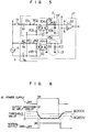
- Fig. 9 shows a block diagram of the conventional PC to which a power supply for AC input is connected.
- the PC 120 is composed of an input section 101 for taking in a signal from an external input device (not shown), an output section 2 for driving an external load (not shown), a memory section 5 including a system memory portion 5a for storing a system program and a program memory 5b for storing a control program, an operating section or central processing unit (hereinafter referred to as CPU) for performing an operation in accordance with the control program, and a power supply section 6.
- the input section 101 has a common terminal 101c and a plurality of input terminals.
- One side of a single-phase AC power supply 4 for AC input is connected to the common terminal 101c, and the other side of the power supply 4 is connected to the input terminals 101d through switches 1s provided in the external input device.
- switches 1s provided in the external input device.
- Fig. 10 is a timing chart concerning the AC input in the prior art.
- a waveform A shows the behavior of the AC power supply 4.
- An A1 portion of the waveform A corresponds to the time of instantaneous cut-off of the AC power supply 4, and an A2 portion thereof corresponds to the case where all power supplies including the power supply section 6 are turned off when the switch 1s is in an ON condition.
- a waveform B shows the ON/OFF condition of the switch 1s.
- a waveform C shows the run/stop condition of the PC 120.
- a waveform D shows an input signal taken in the PC 120.
- a D1 portion of the waveform D represents a normal input signal based on the OFF condition of the switch 1s when the AC power supply 4 is in an ON condition, and a D2 portion thereof represents an erroneous input generated in the case where the AC power supply 4 is cut off when the switch 1s is in the ON state.
- a waveform E shows a signal taken in the PC 120 in the case where a counter-measure by the addition of a timer is implemented.
- An E1 portion of the waveform E represents a normal OFF signal.
- an input signal taken in the PC 120 when the switch 1s is turned off in a state in which the AC power supply 4 is in an ON condition, exhibits an OFF signal normally inputted, as shown by the waveform D.
- the input signal taken in the PC 120 exhibits an OFF signal or erroneous input signal as shown by the D2 portion of the waveform D, notwithstanding that the switch 1s is in an ON condition, as shown by the waveform B.
- a timer circuit is set or added to a control program as a countermeasure for the above problem so that an input is regarded as being a normal OFF signal in the case where the OFF time or duration of a input signal taken in the PC 120 is equal to or longer than a timer time-up time of and as being an erroneous input signal in the case where the former is shorter than the latter.
- a timer circuit 17 is added to a control program so that the timer is operated by a timer contact 18 each time an AC input OFF enters from an AC input signal 16.
- the OFF signal is regarded as being a normal AC power supply OFF signal.
- the PC is operated such that the input is continuously made or the OFF signal is regarded as being an erroneous input when T > D2 (T: a set operating time of the timer) and the OFF signal is regarded as being a normal OFF signal when T ⁇ D1.
- T a set operating time of the timer
- the waveform E of Fig. 10 shows a taken-in signal after the countermeasure by the addition of the timer and E1 shows a normal OFF signal.
- the threshold value for an AC input voltage is set to a value which is about a half of the voltage of the power supply for AC input. Therefore, in the prior art, a plurality of types of input circuit must be prepared according to the power supply voltage for AC input signal, e.g., in Japan, for 100 V circuit and for 200 V circuit.
- Figs. 12A and 12B show the input versus output characteristics of the circuit for AC 100 V and the circuit for AC 200 V, respectively.
- An object of the present invention is to provide a programmable controller (PC) including an input circuit in which not only an erroneous input can be prevented by connecting a line to a power supply for AC input signal from an external input device, thereby to detect the cut-off of the power supply for AC input of the external input device and holding the ON/OFF condition of an input signal before the cut-off of the power supply for AC input during a period of time when the power supply for AC input is an OFF condition but also the application to different input voltages for such a wide input voltage range as, e.g. 100-200 V, is enabled by detecting a voltage of the power supply for AC input of the external input device to automatically determine a proper threshold value level.
- PC programmable controller
- a programmable controller comprising a memory section for storing a control program, an operating section connected to the storage section for performing an operation in accordance with the control program, an input section connected to the operating section for taking in a make/break signal of a contact provided in an external input device, and an output section connected to the operating section for outputting a signal to drive an external load
- the input section includes a first input terminal connected to a power supply which supplies a voltage to the contact, a second input terminal to which the make/break (ON/OFF) signal of the contact is inputted through the contact from the power supply, a first circuit connected to the first input terminal for generating a first signal corresponding to a normal condition of the power supply and a second signal corresponding to an abnormal condition of the power supply, a second circuit connected to the second input terminal for converting a signal inputted through the contact into a third signal corresponding to the make/break of the contact, and an input data hold circuit connected to an output of the second circuit for
- the input section further includes a reference value generation circuit connected to the first input terminal for generating a reference value based on an input voltage value of the power source in the normal condition and a comparator connected to the reference value generation circuit for comparing the output of the second circuit with the reference value, the output of the second circuit being supplied through the comparator to the input data hold circuit.
- the input data hold circuit since in preventing an erroneous input at the time of OFF of the power supply for AC input, the input data hold circuit holds a signal corresponding to the make/break of the contact when a signal corresponding to a cut-off condition of the power supply for AC input is received, it is possible to prevent a time lag of take-in of an input OFF signal and to input even a short input signal, thereby allowing a high-reliability control.
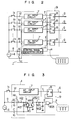
- Fig. 1 is a block diagram showing the construction of a programmable controller (PC) according to an embodiment of the present invention.
- the PC 20 is composed of an input section 1 for taking in a signal from an external input device (not shown), an output section 2 for outputting a signal which drives an external load (not shown), a memory section 5 including a system memory portion 5a for storing a system program and a program memory 5b for storing a control program, an operating section or central processing unit 3 (hereinafter referred to as CPU) for performing an operation in accordance with the control program, and a power supply section 6.
- CPU central processing unit
- the input section 1 has a common terminal 1c as a common input terminal to which one side of a single-phase AC power supply 4 for AC input for supplying a voltage to switches 1s as contacts is connected, a plurality of input terminals 1d as a second input terminal to which make/break (ON/OFF) signals of the switches 1s are inputted through the switches 1s from the other side of the AC power supply 4, and an AC input terminal 1a as a first input terminal which is connected to the other side of the AC power supply 4.
- the switch 1s is provided in the external input device and a signal from the external input device is transmitted in the form of ON/OFF of the switch 1s to the input section 1 through the corresponding input terminal 1d. When the switch 1s is turned on in such a state, a voltage of the AC power source 4 is applied to the corresponding input terminal 1d, thereby resulting in an input as an ON signal.
- connection between the input section 1 and the CPU 3, the connection between the system memory portion 5a and the CPU 3, the connection between the program memory 5b and the CPU 3, and the connection between the output section 2 and the CPU 3 are made by buses (shown by thick arrows in Fig. 1), respectively.
- the power supply section 6 supplies electric powers necessary for operating the input section 1, the output section 2, the system memory portion 5a, the program memory 5b and the CPU 3, respectively.
- the input section 1 in the present embodiment includes AC input circuits 7 as a second circuit which are connected to the common terminal 1c and the input terminals 1d, an erroneous input prevention and threshold value control circuit 14 (hereinafter referred to as control signal generation circuit) as a first circuit which is connected to the common terminal 1c and the AC input terminal 1a, comparators 12 which make the ON/OFF judgement for the outputs of the AC input circuits 7 on the basis of a signal level from the control signal generation circuit 14, and input data hold circuits 8 which hold the outputs of comparators 12 at the timing of a signal from the control signal generation circuit 14 and the outputs of which are connected to the CPU 3 through the bus.
- control signal generation circuit an erroneous input prevention and threshold value control circuit 14 (hereinafter referred to as control signal generation circuit) as a first circuit which is connected to the common terminal 1c and the AC input terminal 1a
- comparators 12 which make the ON/OFF judgement for the outputs of the AC input circuits 7 on the basis of a signal level from the
- a threshold value control circuit 11 is constructed by the control signal generation circuit 14 and the comparators 12, and an erroneous input prevention circuit 9 is constructed by the control signal generation circuit 14 and the input data hold circuits 8.
- the AC input circuit 7 and the threshold value control circuit 11 will be explained using Figs. 5, 6 and 7.
- the AC input circuit 7 includes a signal isolation portion and a voltage level generation portion, as shown in Fig. 5.
- the signal isolation portion is composed of a series circuit which includes a capacitor 701 and a resistor 702 connected between the input terminal 1d and the common terminal 1c and a parallel circuit which includes the primary side (or light emitter side) of a photo coupler 10' and a resistor 703 connected in series with the series circuit.
- the capacitor 701 is provided for limiting an input current
- the resistor 702 is provided for limiting a rush current upon input ON.
- the primary side of the photo coupler 10' has light emitting diodes connected in parallel to each other and in reverse directions and emits light for a signal of either positive or negative direction.
- the resistor 703 is a resistor for input sensitivity adjustment and causes the light emitting diode to emit light in accordance with a voltage division ratio to the impedance of the series circuit of the capacitor 701 and the resistor 702 when a voltage between the input terminal 1d and the common terminal 1c is equal to or higher than a predetermined voltage.
- the capacitor 701 has the impedance of several-ten kilo-ohms and the resistors 702 and 703 have the resistance values of several-hundred ohms and several kilo-ohms, respectively, thereby setting the circuit constant so that a current of about 10 mA flows through the primary side of the photo coupler 10' for an input voltage of 100 V or 200 V.
- the secondary side of the photo coupler 10' includes a photo diode which has an emitter grounded and a collector connected to a power supply voltage + 5 V through a resistor 704.
- the resistor 704 is provided for supplying a high level of the output of the photo coupler.
- the primary and secondary sides can be isolated from each other by use of the photo coupler 10'. Thereby, an AC waveform inputted from the primary side can be transmitted as a full-wave rectified waveform to the secondary side by the photo coupler 10'.
- an integrating circuit 13' including a resistor 705 and a capacitor 706 is connected to the collector of the photo coupler 10' for integrating the output of the photo coupler 10' to provide a voltage level which is to be outputted.
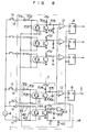
- the control signal generation circuit 14 includes a signal isolation portion, a pulse generation portion and a reference voltage level generation portion, as shown in Fig. 8.
- the threshold value control circuit 11 includes the signal isolation portion and the reference voltage level generation portion of the control signal generation circuit 14 and further includes the comparator 12 connected to the reference voltage level generation portion.
- the signal isolation portion of the threshold value control circuit 11 is composed of a series circuit which includes a capacitor 141 and a resistor 142 connected between the AC input terminal 1a and the common terminal 1c and a parallel circuit which includes the primary side (or light emitter side) of a photo coupler 10 and a resistor 143 connected in series with the series circuit.
- the capacitor 141 is provided for limiting an input current
- the resistor 142 is provided for limiting a rush current upon input ON.
- the primary side of the photo coupler 10 has light emitting diodes connected in parallel to each other and in reverse directions and emits light for a signal of either positive or negative direction.
- the resistor 143 is a resistor for input sensitivity adjustment and causes the light emitting diode to emit light in accordance with a voltage division ratio to the impedance of the series circuit of the capacitor 141 and the resistor 142 when a voltage between the AC input terminal 1a and the common terminal 1c is equal to or higher than a predetermined voltage.
- the capacitor 141 has the impedance of several-ten kilo-ohms and the resistors 142 and 143 have the resistance values of several-hundred ohms and several kilo-ohms, respectively, thereby setting the circuit constant so that a current of about 10 mA flows through the primary side of the photo coupler 10 for an input voltage of 100 V or 200 V.
- the secondary side of the photo coupler 10 includes a photo diode which has an emitter grounded and a collector connected to a power supply voltage + 5 V through a resistor 144.
- the resistor 144 is provided for supplying a high level of the output of the photo coupler.
- the primary and secondary sides can be isolated from each other by use of the photo coupler 10. Thereby, the photo coupler 10 can transmit an AC input a on the primary side thereof to the secondary side thereof as a full-wave rectified waveform b .
- an integrating circuit 13 including a resistor 111 and a capacitor 112 is connected to the collector of the photo coupler 10.
- the output of the photo coupler 10' is connected to a plus-side input terminal of the comparator 12.
- the output of the AC input circuit 7 is connected to a minus-side input terminal of the comparator 12.
- the threshold value control circuit 11 has a function of automatically setting a threshold value. This function will now be explained.
- a voltage from the power supply 4 for AC input is applied as an input to the threshold value control circuit 11 and this input signal is transmitted to the secondary side of the photo coupler 10.
- the integrating circuit 13 extracts DC components.
- a integration time constant of the integrating circuit 13 is made large so that ripple voltages are removed and a variation in output level is minimized even if the power supply 4 for AC input is instantaneously cut off.
- a DC level of the output of the integrating circuit 13 changes in accordance with the voltage of the power supply 4 for AC input which is inputted.
- the photo coupler 10 transmits a portion of a full-wave rectified waveform on the primary side thereof not higher than 1 V to the secondary side as an OFF signal.
- a time width or duration of the portion not higher than 1 V becomes narrow and a time width of a portion higher than 1 V becomes correspondingly wide. Therefore, on the secondary side of the photo coupler 10, an OFF (or H level) time becomes short while an ON (or L level) time becomes long and hence a DC component as the average of those levels decreases.
- the level of a DC component when the voltage of the power supply 4 for AC input is AC 200 V is different from or lower than the level of a DC component when it is AC 100 V. Therefore, as this level to be taken as a threshold value is lower, an input as ON requires the application of a higher input voltage.
- the comparator 12 compares the output level of the AC input circuit 7 with the output level of the threshold value control circuit 11 as a threshold value to output data of the make/break (ON/OFF) condition of the switch 1s as ON if the AC input circuit 7 is lower than the threshold value and as OFF if it is higher than the threshold value.
- Fig. 6 is a diagram showing a relationship between the output level waveform of the AC input circuit 7, threshold levels and the output of the comparator 12.
- a threshold level for AC 100 V and a threshold level for AC 200 V are different from each other and which level is determined by a voltage value of the power supply 4 for AC input.
- the comparator 12 operates such that it provides an ON output during a period of time when the input level is lower than the threshold value.
- FIG. 2 A block diagram of the erroneous input prevention circuit 9 is shown in Fig. 2.
- the comparator 12 of the threshold value control circuit 11 is omitted from the illustration.
- An input from the AC power supply 4 is applied to the AC input terminal 1a of the input section 1 directly with no intervention of the switch 1s.
- the input data hold circuit 8 connected on the output side of each AC input circuit 7 is a flip-flop circuit.
- the flip-flop circuit holds an output f of each AC input circuit 7 as input data.
- the control signal generation circuit 14 On the basis of the output of the AC power supply 4 applied to the AC input terminal 1a, the control signal generation circuit 14 generates a pulse signal e as a first signal a normal condition of the AC power supply 4.
- This pulse signal e is supplied to a clock terminal of each flip-flop circuit so that it is used for updating of the held data. Therefore, when the AC power supply is turned off, the output of the control signal generation circuit 14 becomes an L level signal as a second signal corresponding to the cut-off condition of the AC power supply 4 or generates no pulse signal e so that the data held by the flip-flop circuit is not updated. Thereby, each hold circuit 8 holds input data from the corresponding AC input circuit 7 before updating.
- the control signal generation circuit 14 includes a signal isolation portion, a pulse generation portion and a reference voltage level generation portion, as shown in Fig. 8.
- the erroneous input prevention control circuit 14 includes the signal isolation portion and the reference voltage level generation portion of the control signal generation circuit 14 and further includes the hold circuit 8 connected to the reference voltage level generation portion.
- the signal isolation portion is held in common by the erroneous input prevention control circuit 14 and the threshold value control circuit. Therefore, the explanation of the signal isolation portion of the erroneous input prevention control circuit will be omitted.
- a circuit on the secondary side of a photo coupler 10 includes a two-input NOR gate 903 which has one input connected to a collector of the photo coupler 10 through an integrating circuit including a resistor 901 and a capacitor 902 and the other input connected to the collector of the photo coupler 10 directly.
- An output of the two-input NOR gate 903 is connected to a clock terminal of a flip-flop circuit of the input data hold circuit 8.
- An output f of the AC input circuit 7 is connected to a data input terminal of the flip-flop circuit.
- the operation of the erroneous input prevention circuit 9 will be explained using a control timing chart shown in Figs. 4a-4g.
- the single-phase AC power supply 4 for AC input is connected between the common terminal 1c and the AC input terminal 1a so that an AC waveform shown by a waveform in Fig. 4a is supplied to the erroneous input prevention circuit 9.
- This AC waveform is converted by a capacitor 141 and resistors 142 and 143 into a voltage/current value suitable for causing the emission of light from a light emitter portion of the photo coupler 10.
- the pulses When those pulses are applied to the integrating circuit, the pulses are converted into a DC level with fine pulses being erased, as shown by a waveform in Fig. 4d.
- This DC level shows that an input voltage is applied.
- the integrating circuit is provided for extracting DC components of an output signal of the photo coupler 10 so that the output of the integrating circuit takes an L level when the input is an ON condition and an H level when it is in an OFF condition.
- the NOR circuit inputted with the output of the integrating circuit and the collector output of the photo coupler 10 generates a signal (or a waveform shown in Fig. 4e) which takes an H level when both the waveforms in Figs. 4c and 4d take L levels.
- pulses are not outputted which are sent to the input data hold circuit 8.
- Such pulses are used by the input data hold circuit 8 as pulses for data updating.
- the signal of the photo coupler 10 is transmitted to the input terminal of the NOR gate 903 with a delay time Tc corresponding to a discharging time of the capacitor 902. Therefore, in the case where the AC power supply is cut off due to a power stoppage, the input to the NOR gate 903 is started with a delay of the time Tc immediately from the release from the power stoppage or the restoration of a power supply.
- Fig. 8 shows a circuit diagram showing the construction of the input circuit including the erroneous input prevention circuit and the threshold value control circuit explained above.
- the construction of the control signal generation circuit 14 including a signal isolation portion, a pulse generation portion and a reference voltage level generation portion is simplified by forming the erroneous input prevention circuit 9 and the threshold value control circuit 11 in such a manner that the isolation portion is held in common by them.
- the prevention of an erroneous input upon AC power supply cut-off and the automatic setting of a proper threshold value can be made.
- an input can be made with no delay of an operation and even for a short OFF signal by inputting a voltage of the power supply 4 for AC input as it is, to make a control to prevent an erroneous input signal during a period of time when the power supply is cut off. Also, it becomes possible to cope with a wide voltage range of the power supply 4 for AC input by inputting the voltage of the power supply for AC input, checking the level of the inputted voltage to detect an input voltage range and determining from the detected voltage range or value a proper threshold value (which may be about a half of the voltage of the power supply for AC input).
Landscapes
- Physics & Mathematics (AREA)
- General Physics & Mathematics (AREA)
- Engineering & Computer Science (AREA)
- Automation & Control Theory (AREA)
- Programmable Controllers (AREA)
- Power Sources (AREA)
- Safety Devices In Control Systems (AREA)
Applications Claiming Priority (2)
| Application Number | Priority Date | Filing Date | Title |
|---|---|---|---|
| JP4100881A JPH05297992A (ja) | 1992-04-21 | 1992-04-21 | プログラマブルコントローラの入力回路 |
| JP100881/92 | 1992-04-21 |
Publications (2)
| Publication Number | Publication Date |
|---|---|
| EP0566996A2 true EP0566996A2 (de) | 1993-10-27 |
| EP0566996A3 EP0566996A3 (en) | 1993-11-18 |
Family
ID=14285675
Family Applications (1)
| Application Number | Title | Priority Date | Filing Date |
|---|---|---|---|
| EP19930106154 Withdrawn EP0566996A3 (en) | 1992-04-21 | 1993-04-15 | Programmable controller with erroneous input prevention control circuit |
Country Status (2)
| Country | Link |
|---|---|
| EP (1) | EP0566996A3 (de) |
| JP (1) | JPH05297992A (de) |
Cited By (2)
| Publication number | Priority date | Publication date | Assignee | Title |
|---|---|---|---|---|
| US6714996B1 (en) * | 1999-08-30 | 2004-03-30 | Mitsubishi Denki Kabushiki Kaisha | Programmable controller system and method for resetting programmable controller system |
| CN110641158A (zh) * | 2019-11-06 | 2020-01-03 | 北海绩迅电子科技有限公司 | 一种墨盒注墨装置 |
Families Citing this family (4)
| Publication number | Priority date | Publication date | Assignee | Title |
|---|---|---|---|---|
| JP4541981B2 (ja) * | 2005-06-28 | 2010-09-08 | 株式会社日立産機システム | 開閉情報取得装置 |
| JP2009129238A (ja) * | 2007-11-26 | 2009-06-11 | Hitachi Industrial Equipment Systems Co Ltd | プログラマブルコントローラ |
| JP2013134561A (ja) * | 2011-12-26 | 2013-07-08 | Hitachi Industrial Equipment Systems Co Ltd | プログラマブルコントローラ |
| JP2020046955A (ja) * | 2018-09-19 | 2020-03-26 | 株式会社東芝 | Ac入力装置 |
Family Cites Families (4)
| Publication number | Priority date | Publication date | Assignee | Title |
|---|---|---|---|---|
| FR2607274B1 (fr) * | 1986-11-25 | 1989-03-31 | Telemecanique Electrique | Circuit de gestion d'entrees notamment pour automate programmable |
| US4910659A (en) * | 1987-12-11 | 1990-03-20 | Square D Company | Input and output peripheral controller cards for use in a programmable logic controller system |
| JPH03217904A (ja) * | 1990-01-23 | 1991-09-25 | Toshiba Mach Co Ltd | 入力モジュール |
| JPH03268006A (ja) * | 1990-03-19 | 1991-11-28 | Hitachi Ltd | プログラマブルコントローラ |
-
1992
- 1992-04-21 JP JP4100881A patent/JPH05297992A/ja active Pending
-
1993
- 1993-04-15 EP EP19930106154 patent/EP0566996A3/en not_active Withdrawn
Cited By (3)
| Publication number | Priority date | Publication date | Assignee | Title |
|---|---|---|---|---|
| US6714996B1 (en) * | 1999-08-30 | 2004-03-30 | Mitsubishi Denki Kabushiki Kaisha | Programmable controller system and method for resetting programmable controller system |
| CN110641158A (zh) * | 2019-11-06 | 2020-01-03 | 北海绩迅电子科技有限公司 | 一种墨盒注墨装置 |
| CN110641158B (zh) * | 2019-11-06 | 2024-05-07 | 北海绩迅科技股份有限公司 | 一种墨盒注墨装置 |
Also Published As
| Publication number | Publication date |
|---|---|
| EP0566996A3 (en) | 1993-11-18 |
| JPH05297992A (ja) | 1993-11-12 |
Similar Documents
| Publication | Publication Date | Title |
|---|---|---|
| US4962350A (en) | Load condition detecting and driving system | |
| US7280333B2 (en) | Method and device for short circuit or open load detection | |
| EP0192832B1 (de) | Fehlerdetektor mit Mehrfachfunktion für einen Drehstromgenerator | |
| JPH0942129A (ja) | 内燃機関の点火装置 | |
| EP0118779B1 (de) | Spannungsregler für einen Ladegenerator | |
| US5936361A (en) | Discharge lamp lighting circuit with lighting condition detector | |
| US6327130B1 (en) | Control device of a circuit breaker opening or closing electromagnet with local and remote control | |
| EP0020098A1 (de) | Steuervorrichtung für die Spannungserzeugung durch Fahrzeuggeneratoren | |
| US5426776A (en) | Microprocessor watchdog circuit | |
| EP0566996A2 (de) | Speicherprogrammierbare Steuerung mit einem Schaltkreis zur Vermeidung von falschen Eingaben | |
| CA2013296C (en) | Memory drive device and method | |
| US4864163A (en) | Method for detecting input AC voltage | |
| GB2115966A (en) | Fire alarm system | |
| JP2793909B2 (ja) | 組合わせ入出力点を有する入出力モジュール | |
| US4009420A (en) | Solid state power controller | |
| US4438384A (en) | Generation indicating apparatus for vehicle alternators | |
| US4903011A (en) | Lamp drive circuit | |
| US6944003B2 (en) | Semiconductor integrated circuit with voltage-detecting circuit and signal transmitting and receiving system | |
| EP0250932A1 (de) | Energieversorgungssystem | |
| US4355239A (en) | Electrical power supply arrangement | |
| JP2546019B2 (ja) | 停電検出回路 | |
| JPH05252673A (ja) | 電源装置 | |
| JPH0345795B2 (de) | ||
| JP2603778B2 (ja) | 多重伝送システムの端末器 | |
| JPH0142054Y2 (de) |
Legal Events
| Date | Code | Title | Description |
|---|---|---|---|
| PUAI | Public reference made under article 153(3) epc to a published international application that has entered the european phase |
Free format text: ORIGINAL CODE: 0009012 |
|
| PUAL | Search report despatched |
Free format text: ORIGINAL CODE: 0009013 |
|
| AK | Designated contracting states |
Kind code of ref document: A2 Designated state(s): CH DE IT LI |
|
| AK | Designated contracting states |
Kind code of ref document: A3 Designated state(s): CH DE IT LI |
|
| 17P | Request for examination filed |
Effective date: 19940422 |
|
| 17Q | First examination report despatched |
Effective date: 19951106 |
|
| 18D | Application deemed to be withdrawn |
Effective date: 19960319 |